


Last Edited by SP 14112004
CHAPTER 10
VHDL
The U.S. Department of Defense (DoD) supported the development of VHDL (VHSIC hardware description language) as part of the VHSIC (very high-speed IC) program in the early 1980s. The companies in the VHSIC program found they needed something more than schematic entry to describe large ASICs, and proposed the creation of a hardware description language. VHDL was then handed over to the Institute of Electrical and Electronics Engineers (IEEE) in order to develop and approve the IEEE Standard 1076-1987. 1 As part of its standardization process the DoD has specified the use of VHDL as the documentation, simulation, and verification medium for ASICs (MIL-STD-454). Partly for this reason VHDL has gained rapid acceptance, initially for description and documentation, and then for design entry, simulation, and synthesis as well.
The first revision of the 1076 standard was approved in 1993. References to the VHDL Language Reference Manual (LRM) in this chapter--[VHDL 87LRM2.1, 93LRM2.2] for example--point to the 1987 and 1993 versions of the LRM [IEEE, 1076-1987 and 1076-1993]. The prefixes 87 and 93 are omitted if the references are the same in both editions. Technically 1076-1987 (known as VHDL-87) is now obsolete and replaced by 1076-1993 (known as VHDL-93). Except for code that is marked 'VHDL-93 only' the examples in this chapter can be analyzed (the VHDL word for "compiled") and simulated using both VHDL-87 and VHDL-93 systems.
1. Some of the material in this chapter is reprinted with permission from IEEE Std 1076-1993, © 1993 IEEE. All rights reserved.
10.1 A Counter
The following VHDL model describes an electrical "black box" that contains a 50 MHz clock generator and a counter. The counter increments on the negative edge of the clock, counting from zero to seven, and then begins at zero again. The model contains separate processes that execute at the same time as each other. Modeling concurrent execution is the major difference between HDLs and computer programming languages such as C.
entity Counter_1 is end; -- declare a "black box" called Counter_1 library STD; use STD.TEXTIO.all; -- we need this library to print architecture Behave_1 of Counter_1 is -- describe the "black box"
--declare a signal for the clock, type BIT, initial value '0' signal Clock : BIT := '0';
--declare a signal for the count, type INTEGER, initial value 0
signal Count : INTEGER := 0;
begin
process begin -- process to generate the clock
wait for 10 ns; -- a delay of 10 ns is half the clock cycle Clock <= not Clock;
if (now > 340 ns) then wait; end if; -- stop after 340 ns end process;
--process to do the counting, runs concurrently with other processes process begin
--wait here until the clock goes from 1 to 0
wait until (Clock = '0'); -- now handle the counting
if (Count = 7) then Count <= 0; else Count <= Count + 1;
end if; end process;
process (Count) variable L: LINE; begin -- process to print write(L, now); write(L, STRING'(" Count=")); write(L, Count); writeline(output, L);
end process;
end;
Throughout this book VHDL keywords (reserved words that are part of the language) are shown in bold type in code examples (but not in the text). The code examples use the bold keywords to improve readability. VHDL code is often lengthy and the code in this book is always complete wherever possible. In order to save space many of the code examples do not use the conventional spacing and formatting that is normally considered good practice. So "Do as I say and not as I do."
The steps to simulate the model and the printed results for Counter_1 using the Model Technology V-System/Plus common-kernel simulator are as follows:
>vlib work
>vcom Counter_1.vhd
Model Technology VCOM V-System VHDL/Verilog 4.5b
--Loading package standard
--Compiling entity counter_1
--Loading package textio
--Compiling architecture behave_1 of counter_1 > vsim -c counter_1
# Loading /../std.standard
# Loading /../std.textio(body)
# Loading work.counter_1(behave_1) VSIM 1> run 500
# 0 ns Count=0
# 20 ns Count=1
(...15 lines omitted...)
# 340 ns Count=1 VSIM 2> quit
10.2 A 4-bit Multiplier
This section presents a more complex VHDL example to motivate the study of the syntax and semantics of VHDL in the rest of this chapter.
10.2.1 An 8-bit Adder
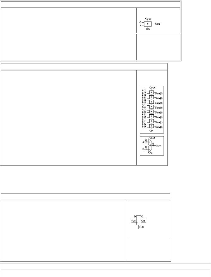
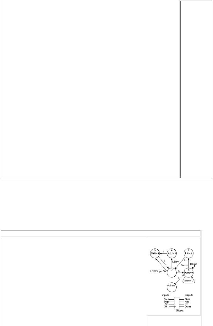
Table 10.1 shows a VHDL model for the full adder that we described in Section 2.6, "Datapath Logic Cells." Table 10.2 shows a VHDL model for an 8-bit ripple-carry adder that uses eight instances of the full adder.
10.2.2 A Register Accumulator
Table 10.3 shows a VHDL model for a positive-edge-triggered D flip-flop with an active-high asynchronous clear. Table 10.4 shows an 8-bit register that uses this D flip-flop model (this model only provides the Q output from the register and leaves the QN flip-flop outputs unconnected).
Table 10.5 shows a model for a datapath multiplexer that consists of eight 2:1 multiplexers with a common select input (this select signal would normally be a control signal in a datapath). The multiplier will use the register and multiplexer components to implement a register accumulator.
10.2.3 Zero Detector
Table 10.6 shows a model for a variable-width zero detector that accepts a bus of any width and will produce a single-bit output of '1' if all input bits are zero.
10.2.4 A Shift Register
Table 10.7 shows a variable-width shift register that shifts (left or right under input control, DIR ) on the positive edge of the clock, CLK , gated by a shift enable, SH . The parallel load, LD , is synchronous and aligns the input LSB to the LSB of the output, filling unused MSBs with zero. Bits vacated during shifts are zero filled. The clear, CLR , is asynchronous.
10.2.5 A State Machine
To multiply two binary numbers A and B , we can use the following algorithm:
If the LSB of A is '1', then add B into an accumulator.
Shift A one bit to the right and B one bit to the left.
Stop when all bits of A are zero.
Table 10.8 shows the VHDL model for a Moore (outputs depend only on the state) finite-state machine for the multiplier, together with its state diagram.
10.2.6 A Multiplier
Table 10.9 shows a schematic and the VHDL code that describes the interconnection of all the components for the multiplier. Notice that the schematic comprises two halves: an 8-bit-wide datapath section (consisting of the registers, adder, multiplexer, and zero detector) and a control section (the finite-state machine). The arrows in the schematic denote the inputs and outputs of each component. As we shall see in Section 10.7, VHDL has strict rules about the direction of connections.
10.2.7 Packages and Testbench
To complete and test the multiplier design we need a few more items. First we need the following "components list" for the items in Table 10.9:
package Mult_Components is
component Mux8 port (A,B:BIT_VECTOR(7 downto 0); Sel:BIT;Y:out BIT_VECTOR(7 downto 0));end component;
component AllZero port (X : BIT_VECTOR; F:out BIT );end component;
component Adder8 port (A,B:BIT_VECTOR(7 downto 0);Cin:BIT;
Cout:out BIT;Sum:out BIT_VECTOR(7 downto 0));end component; component Register8 port (D:BIT_VECTOR(7 downto 0);
Clk,Clr:BIT; Q:out BIT_VECTOR(7 downto 0));end component; component ShiftN port (CLK,CLR,LD,SH,DIR:BIT;D:BIT_VECTOR;
Q:out BIT_VECTOR);end component;
component SM_1 port (Start,CLK,LSB,Stop,Reset:BIT; Init,Shift,Add,Done:out BIT);end component;
end;
Next we need some utility code to help test the multiplier. The following VHDL generates a clock with programmable "high" time ( HT ) and "low" time ( LT ):
package Clock_Utils is
procedure Clock (signal C: out Bit; HT, LT:TIME); end Clock_Utils;
package body Clock_Utils is
procedure Clock (signal C: out Bit; HT, LT:TIME) is begin
loop C<='1' after LT, '0' after LT + HT; wait for LT + HT; end loop;
end;
end Clock_Utils;
Finally, the following code defines two functions that we shall also use for testing--the functions convert an array of bits to a number and vice versa:
package Utils is
function Convert (N,L: NATURAL) return BIT_VECTOR; function Convert (B: BIT_VECTOR) return NATURAL;
end Utils;
package body Utils is
function Convert (N,L: NATURAL) return BIT_VECTOR is variable T:BIT_VECTOR(L-1 downto 0); variable V:NATURAL:= N;
begin for i in T'RIGHT to T'LEFT loop
T(i) := BIT'VAL(V mod 2); V:= V/2; end loop; return T;
end;
function Convert (B: BIT_VECTOR) return NATURAL is variable T:BIT_VECTOR(B'LENGTH-1 downto 0) := B; variable V:NATURAL:= 0;
begin for i in T'RIGHT to T'LEFT loop
if T(i) = '1' then V:= V + (2**i); end if; end loop; return V;
end;
end Utils;
The following code tests the multiplier model. This is a testbench (this simple example is not a comprehensive test). First we reset the logic (line 17) and then apply a series of values to the inputs, A and B . The clock generator (line 14) supplies a clock with a 20 ns period. The inputs are changed 1 ns after a positive clock edge, and remain stable for 20 ns through the next positive clock edge.
entity Test_Mult8_1 is end; -- runs forever, use break!! architecture Structure of Test_Mult8_1 is
use Work.Utils.all; use Work.Clock_Utils.all; component Mult8 port
(A, B : BIT_VECTOR(3 downto 0); Start, CLK, Reset : BIT; Result : out BIT_VECTOR(7 downto 0); Done : out BIT);
end component;
signal A, B : BIT_VECTOR(3 downto 0); signal Start, Done : BIT := '0'; signal CLK, Reset : BIT;
signal Result : BIT_VECTOR(7 downto 0); signal DA, DB, DR : INTEGER range 0 to 255; begin
C: Clock(CLK, 10 ns, 10 ns);
UUT: Mult8 port map (A, B, Start, CLK, Reset, Result, Done); DR <= Convert(Result);
Reset <= '1', '0' after 1 ns; process begin
for i in 1 to 3 loop for j in 4 to 7 loop
DA <= i; DB <= j; A<=Convert(i,A'Length);B<=Convert(j,B'Length); wait until CLK'EVENT and CLK='1'; wait for 1 ns;
Start <= '1', '0' after 20 ns; wait until Done = '1'; wait until CLK'EVENT and CLK='1';
end loop; end loop;
for i in 0 to 1 loop for j in 0 to 15 loop
DA <= i; DB <= j;

A<=Convert(i,A'Length);B<=Convert(j,B'Length); wait until CLK'EVENT and CLK='1'; wait for 1 ns;
Start <= '1', '0' after 20 ns; wait until Done = '1'; wait until CLK'EVENT and CLK='1';
end loop; end loop; wait;
end process; end;
Here is the signal trace output from the Compass Scout simulator:
Time(fs) + Cycle |
da |
|
db |
|
dr |
|
---------------------- ------------ |
------------ |
------------ |
||||
0+ |
0: |
0 |
|
0 |
|
0 |
0+ |
1: * |
1 |
* |
4 |
* |
0 |
... |
|
|
|
|
|
|
92000000+ |
3: |
1 |
|
4 |
* |
4 |
... |
|
|
|
|
|
|
150000000+ |
1: * |
1 |
* |
5 |
|
4 |
... |
|
|
|
|
|
|
193000000+ |
3: |
1 |
|
5 |
* |
0 |
... |
|
|
|
|
|
|
252000000+ |
3: |
1 |
|
5 |
* |
5 |
... |
|
|
|
|
|
|
310000000+ |
1: * |
1 |
* |
6 |
|
5 |
... |
|
|
|
|
|
|
353000000+ |
3: |
1 |
|
6 |
* |
0 |
... |
|
|
|
|
|
|
412000000+ |
3: |
1 |
|
6 |
* |
6 |
Positive clock edges occur at 10, 30, 50, 70, 90, ... ns. You can see that the output (dr) changes from '0' to '4' at 92 ns, after five clock edges (with a 2 ns delay due to the output register, R1).