

3.4 Library-Cell Design
The optimum cell layout for each process generation changes because the design rules for each ASIC vendor s process are always slightly different even for the same generation of technology. For example, two companies may have very similar 0.35 m m CMOS process technologies, but the third-level metal spacing might be slightly different. If a cell library is to be used with both processes, we could construct the library by adopting the most stringent rules from each process. A library constructed in this fashion may not be competitive with one that is constructed specifically for each process. Even though ASIC vendors prize their design rules as secret, it turns out that they are similar except for a few details. Unfortunately, it is the details that stop us moving designs from one process to another. Unless we are a very large customer it is difficult to have an ASIC vendor change or waive design rules for us. We would like all vendors to agree on a common set of design rules. This is, in fact, easier than it sounds. The reason that most vendors have similar rules is because most vendors use the same manufacturing equipment and a similar process. It is possible to construct a highest common denominator library that extracts the most from the current manufacturing capability. Some library companies and the large Japanese ASIC vendors are adopting this approach.
Layout of library cells is either hand-crafted or uses some form of symbolic layout . Symbolic layout is usually performed in one of two ways: using either interactive graphics or a text layout language. Shapes are represented by simple lines or rectangles, known as sticks or logs , in symbolic layout. The actual dimensions of the sticks or logs are determined after layout is completed in a postprocessing step. An alternative to graphical symbolic layout uses a text layout language, similar to a programming language such as C, that directs a program to assemble layout. The spacing and dimensions of the layout shapes are defined in terms of variables rather than constants. These variables can be changed after symbolic layout is complete to adjust the layout spacing to a specific process.
Mapping symbolic layout to a specific process technology uses 10 20 percent more area than hand-crafted layout (though this can then be further reduced to 510 percent with compaction). Most symbolic layout systems do not allow 45° layout and this introduces a further area penalty (my experience shows this is about 5 15 percent). As libraries get larger, and the capability to quickly move libraries and ASIC designs between different generations of process technologies becomes more important, the advantages of symbolic layout may outweigh the disadvantages.
3.5 Library Architecture
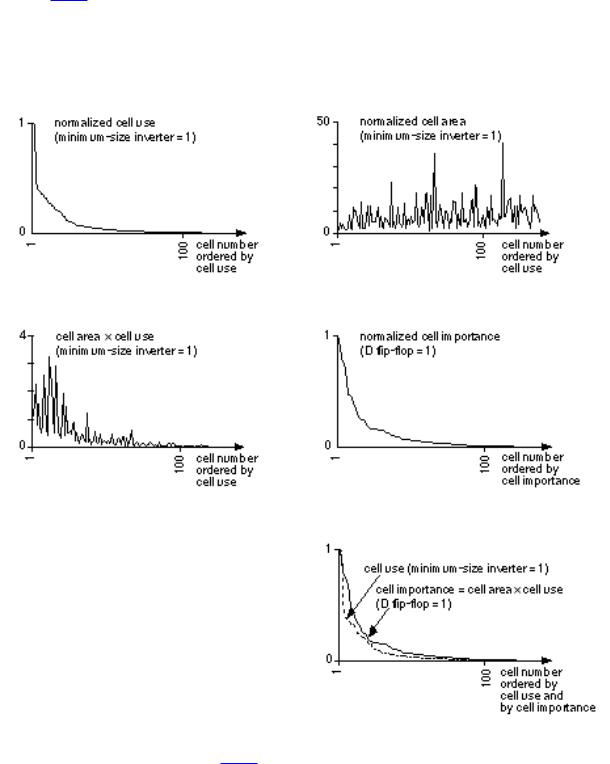
Figure 3.13 (a) shows cell use data from over 150 CMOS gate array designs.
These results are remarkably similar to that from other ASIC designs using different libraries and different technologies and show that typically 80 percent of an ASIC uses less than 20 percent of the cell library.
(a) |
(b ) |
(c) |
(d) |
(e )
FIGURE 3.13 Cell library statistics.
We can use the data in Figure 3.13 (a) to derive some useful conclusions about the
number and types of cells to be included in a library. Before we do this, a few
words of caution are in order. First, the data shown in Figure 3.13 (a) tells us about
cells that are included a library. This data cannot tell us anything about cells that are not (and perhaps should be) included in a library. Second, the type of design entry we use and the type of ASIC we are designing can dramatically affect the profile of the use of different cell types. For example, if we use a high-level design language, together with logic synthesis, to enter an ASIC design, this will favor the use of the complex combinational cells (cells of the AOI family that are particularly area efficient in CMOS, but are difficult to work with when we design by hand).
Figure 3.13 (a) tells us which cells we use most often, but does not take into
account the cell area. What we really want to know are which cells are most important in determining the area of an ASIC. Figure 3.13 (b) shows the area of
the cells normalized to the area of a minimum-size inverter. If we take the data in Figure 3.13 (a) and multiply by the cell areas, we can derive a new measure of the
contribution of each cell in a library (Figure 3.13c). This new measure, cell importance , is a measure of how much area each cell in a library contributes to a typical ASIC. For example, we can see from Figure 3.13 (c) that a D flip-flop
(with a cell importance of 3.5) contributes 3.5 times as much area on a typical ASIC than does an inverter (with a cell importance of 1).
Figure 3.13 (c) shows cell importance ordered by the cell frequency of use and
normalized to an inverter. We can rearrange this data in terms of cell importance, as shown in Figure 3.13 (d), and normalized so that now the most important cell, a
D flip-flop, has a cell importance of 1. Figure 3.13 (e) includes the cell use data on
the same scale as the cell importance data. Both show roughly the same shape, reflecting that both measures obey an 80 20 rule. Roughly 20 percent of the cells in a library correspond to 80 percent of the ASIC area and 80 percent of the cells we use (but not the same 20 percent that is why cell importance is useful).
Figure 3.13 (e) shows us that the most important cells, measured by their
contribution to the area of an ASIC, are not necessarily the cells that we use most often. If we wish to build or buy a dense library, we must concentrate on the area of those cells that have the highest cell importance not the most common cells.

3.6 Gate-Array Design
Each logic cell or macro in a gate-array library is predesigned using fixed tiles of transistors known as the gate-array base cell (or just base cell ). We call the arrangement of base cells across a whole chip in a complete gate array the gate-array base (or just base ). ASIC vendors offer a selection of bases, with a different total numbers of transistors on each base. For example, if our ASIC design uses 48k equivalent gates and the ASIC vendor offers gate arrays bases with 50k-, 75k-, and 100k-gates, we will probably have to use the 75k-gate base (because it is unlikely that we can use 48/50 or 96 percent of the transistors on the 50k-gate base).
We isolate the transistors on a gate array from one another either with thick field oxide (in the case of oxide-isolated gate arrays) or by using other transistors that are wired permanently off (in gate-isolated gate arrays). Channeled and channelless gate arrays may use either gate isolation or oxide isolation.
Figure 3.14 (a) shows a base cell for a gate-isolated gate array . This base cell
has two transistors: one p -channel and one n -channel. When these base cells are placed next to each other, the n -diffusion and p -diffusion layers form continuous strips that run across the entire chip broken only at the poly gates that cross at regularly spaced intervals (Figure 3.14b). The metal interconnect spacing determines the separation of the transistors. The metal spacing is determined by the design rules for the metal and contacts. In Figure 3.14 (c) we have shown all
possible locations for a contact in the base cell. There is room for 21 contacts in this cell and thus room for 21 interconnect lines running in a horizontal direction (we use m1 running horizontally). We say that there are 21 horizontal tracks in this cell or that the cell is 21 tracks high. In a similar fashion the space that we need for a vertical interconnect (m2) is called a vertical track . The horizontal and vertical track widths are not necessarily equal, because the design rules for m1 and m2 are not always equal.
We isolate logic cells from each other in gate-isolated gate arrays by connecting transistor gates to the supply bus hence the name, gate isolation . If we connect the gate of an n -channel transistor to V SS , we isolate the regions of n -diffusion on each side of that transistor (we call this an isolator transistor or device, or just isolator). Similarly if we connect the gate of a p -channel transistor to V DD , we isolate adjacent p -diffusion regions.
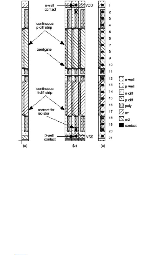
FIGURE 3.14 The construction of a gate-isolated gate array. (a) The one-track-wide base cell containing one p -channel and one n -channel transistor.
(b) Three base cells: the center base cell is being used to isolate the base cells on either side from each other. (c) A base cell including all possible contact positions (there is room for 21 contacts in the vertical direction, showing the base cell has a height of 21 tracks).
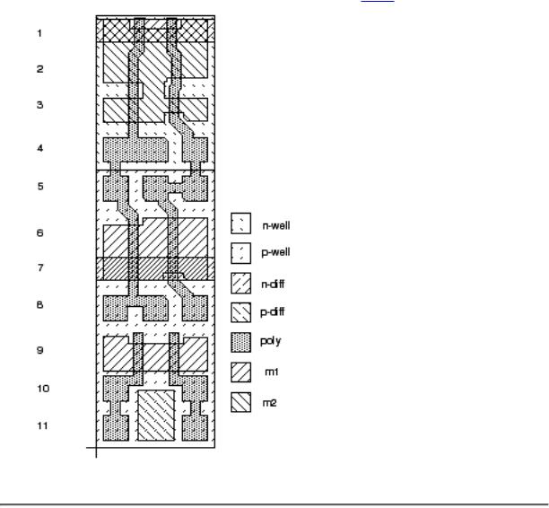
Oxide-isolated gate arrays often contain four transistors in the base cell: the two n -channel transistors share an n -diffusion strip and the two p -channel transistors share a p -diffusion strip. This means that the two n -channel transistors in each base cell are electrically connected in series, as are the p -channel transistors. The base cells are isolated from each other using oxide isolation . During the fabrication process a layer of the thick field oxide is left in place between each base cell and this separates the p -diffusion and n -diffusion regions of adjacent base cells.
Figure 3.15 shows an oxide-isolated gate array . This cell contains eight
transistors (which occupy six vertical tracks) plus one-half of a single track that contains the well contacts and substrate connections that we can consider to be shared by each base cell.
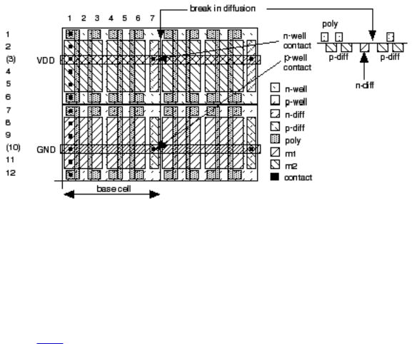
FIGURE 3.15 An oxide-isolated gate-array base cell. The figure shows two base cells, each containing eight transistors and two well contacts. The p -channel and n -channel transistors are each 4 tracks high (corresponding to the width of the transistor). The leftmost vertical track of the left base cell includes all 12 possible contact positions (the height of the cell is 12 tracks). As outlined here, the base cell is 7 tracks wide (we could also consider the base cell to be half this width).
Figure 3.16 shows a base cell in which the gates of the n -channel and p -channel
transistors are connected on the polysilicon layer. Connecting the gates in poly saves contacts and a metal interconnect in the center of the cell where interconnect is most congested. The drawback of the preconnected gates is a loss in flexibility in cell design. Implementing memory and logic based on transmission gates will be less efficient using this type of base cell, for example.

FIGURE 3.16 This oxide-isolated gate-array base cell is 14 tracks high and 4 tracks wide. VDD (tracks 3 and 4) and GND (tracks 11 and 12) are each 2 tracks wide. The metal lines to the left of the cell indicate the 10 horizontal routing tracks (tracks 1, 2, 5 10, 13, 14). Notice that the p -channel and n -channel polysilicon gates are tied together in the center of the cell. The well contacts are short, leaving room for a poly cross-under in each base cell.
Figure 3.17 shows the metal personalization for a D flip-flop macro in a
gate-isolated gate array using a base cell similar to that shown in Figure 3.14 (a).
This macro uses 20 base cells, for a total of 40 transistors, equivalent to 10 gates.
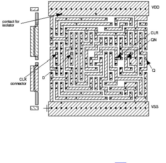
FIGURE 3.17 An example of a flip-flop macro in a gate-isolated gate-array library. Only the first-level metallization and contact pattern (the personalization) is shown on the right, but this is enough information to derive the schematic. The base cell is shown on the left. This macro is 20 tracks wide.
The gates of the base cells shown in Figures 3.14 3.16 are bent. The bent gate
allows contacts to the gates to be placed on the same grid as the contacts to diffusion. The polysilicon gates run in the space between adjacent metal interconnect lines. This saves space and also simplifies the routing software.
There are many trade-offs that determine the gate-array base cell height. One factor is the number of wires that can be run horizontally through the base cell. This will determine the capacity of the routing channel formed from an unused row of base cells. The base cell height also determines how easy it is to wire the logic macros since it determines how much space for wiring is available inside the macros.
There are other factors that determine the width of the base-cell transistors. The widths of the p -channel and n -channel transistors are slightly different in Figure 3.14 (a). The p -channel transistors are 6 tracks wide and the n -channel transistors are 5 tracks wide. The ratio for this gate-array library is thus approximately 1.2. Most gate-array libraries are approaching a ratio of 1.
ASIC designers are using ever-increasing amounts of RAM on gate arrays. It is inefficient to use the normal base cell for a static RAM cell and the size of RAM on an embedded gate array is fixed. As an alternative we can change the design of the base cell. A base cell designed for use as RAM has extra transistors (either four two n -channel and two p -channel or two n -channel; usually minimum
width) allowing a six-transistor RAM cell to be built using one base cell instead of the two or three that we would normally need. This is one of the advantages of the CBA (cell-based array) base cell shown in Figure 3.18 .
FIGURE 3.18 The SiARC/Synopsys cell-based array (CBA) basic cell.