

14.2 Boundary-Scan Test
It is possible to test ICs in dual-in-line packages (DIPs ) with 0.1 inch (2.5 mm) lead spacing on low-density boards using a bed-of-nails tester with probes that contact test points underneath the board. Mechanical testing becomes difficult with board trace widths and separations below 0.1 mm or 100 mm, package-pin separations of 0.3 mm or less, packages with 200 or more pins, surface-mount packages on both sides of the board, and multilayer boards [ Scheiber, 1995].
In 1985 a group of European manufacturers formed the Joint European Test Action Group ( JETAG ) to study board testing. With the addition of North American companies, JETAG became the Joint Test Action Group ( JTAG ) in 1986. The JTAG 2.0 test standard formed the basis of the IEEE Standard 1149.1 Test Port and Boundary-Scan Architecture [ IEEE 1149.1b, 1994], approved in February 1990 and also approved as a standard by the American National Standards Institute (ANSI) in August 1990 [ Bleeker, v. d. Eijnden, and de Jong, 1993; Maunder and Tulloss, 1990; Parker, 1992]. The IEEE standard is still often referred to as JTAG, although there are important differences between the last JTAG specification (version 2.0) and the IEEE 1149.1 standard.
Boundary-scan test ( BST ) is a method for testing boards using a four-wire interface (five wires with an optional master reset signal). A good analogy would be the RS-232 interface for PCs. The BST standard interface was designed to test boards, but it is also useful to test ASICs. The BST interface provides a standard means of communicating with test circuits on-board an ASIC. We do need to include extra circuits on an ASIC in order to use BST. This is an example of increasing the cost and complexity (as well as potentially reducing the performance) of an ASIC to reduce the cost of testing the ASIC and the system.
FIGURE 14.1 IEEE 1149.1 boundary scan. (a) Boundary scan is intended to check for shorts or opens between ICs mounted on a board. (b) Shorts and opens may also occur inside the IC package. (c) The boundary-scan architecture is a long chain of shift registers allowing data to be sent over all the connections between the ICs on a board.
Figure 14.1 (a) illustrates failures that may occur on a PCB due to shorts or opens in the copper traces on the board. Less frequently, failures in the ASIC package may also arise from shorts and opens in the wire bonds between the die and the package frame ( Figure 14.1 b). Failures in an ASIC package that occur during ASIC fabrication are caught by the ASIC production test, but stress during automated handling and board assembly may cause package failures. Figure 14.1 (c) shows how a group of ASICs are linked together in boundary-scan testing. To detect the failures shown in Figure 14.1 (a) or (b) manufacturers use boundary scan to test every connection between ASICs on a board. During boundary scan, test data is loaded into each ASIC and then driven onto the board traces. Each ASIC monitors its inputs, captures the data received, and then shifts the captured data out. Any defects in the board or ASIC connections will show up as a discrepancy between expected and actual measured continuity data.
In order to include BST on an ASIC, we add a special logic cell to each ASIC I/O pad. These cells are joined together to form a chain and create a boundary-scan shift register that extends around each ASIC. The input to a boundary-scan shift register is the test-data input ( TDI ). The output of a boundary-scan shift register is the test-data output ( TDO ). These boundary-scan shift registers are then linked in a serial fashion with the boundary-scan shift registers on other ASICs to form one long boundary-scan shift register. The boundary-scan shift register in each ASIC is one of several test-data registers ( TDR ) that may be included in each ASIC. All the TDRs in an ASIC are connected directly between the TDI and TDO ports. A special register that decodes instructions provides a way to select a particular TDR and control operation of the boundary-scan test process.
Controlling all of the operations involved in selecting registers, loading data, performing a test, and shifting out results are the test clock ( TCK ) and test-mode select ( TMS ). The boundary-scan standard specifies a four-wire test interface using the four signals: TDI, TDO, TCK, and TMS. These four dedicated signals, the test-access port ( TAP ), are connected to the TAP controller inside each ASIC. The TAP controller is a state machine clocked on the rising edge of TCK, and with state transitions controlled by the TMS signal. The test-reset input signal ( TRST* , nTRST , or TRST always an active-low signal) is an optional (fifth) dedicated interface pin to reset the TAP controller.
Normally the boundary-scan shift-register cells at each ASIC I/O pad are transparent, allowing signals to pass between the I/O pad and the core logic. When an ASIC is put into boundary-scan test mode, we first tell the TAP controller which TDR to select. The TAP controller then tells each boundary-scan shift register in the appropriate TDR either to capture input data, to shift data to the neighboring cell, or to output data.
There are many acronyms in the IEEE 1149.1 standard (referred to as dot one );Table 14.3 provides a list of the most common terms.
TABLE 14.3 Boundary-scan terminology. |
|
|
Acronym |
Meaning |
Explanation |
BR |
Bypass register |
A TDR, directly connects TDI and TDO, bypassing BSR |
BSC |
Boundary-scan cell |
Each I/O pad has a BSC to monitor signals |
BSR |
Boundary-scan register |
A TDR, a shift register formed from a chain of BSCs |
BST |
Boundary-scan test |
Not to be confused with BIST (built-in self-test) |
IDCODE |
Device-identification register Optional TDR, contains manufacturer and part number |
|
IR |
Instruction register |
Holds a BST instruction, provides control signals |
JTAG |
Joint Test Action Group |
The organization that developed boundary scan |
TAP |
Test-access port |
Four- (or five-)wire test interface to an ASIC |
TCK |
Test clock |
A TAP wire, the clock that controls BST operation |
TDI |
Test-data input |
A TAP wire, the input to the IR and TDRs |
TDO |
Test-data output |
A TAP wire, the output from the IR and TDRs |
TDR |
Test-data register |
Group of BST registers: IDCODE, BR, BSR |
TMS |
Test-mode select |
A TAP wire, together with TCK controls the BST state |
TRST* or nTRST Test-reset input signal |
Optional TAP wire, resets the TAP controller (active-low) |
|
14.2.1 BST Cells
Figure 14.2 shows a data-register cell ( DR cell ) that may be used to implement any of the TDRs. The most common DR cell is a boundary-scan cell ( BS cell , or BSC ), or boundary-register cell (this last name is not abbreviated to BR cell, since this term is reserved for another type of cell) [ IEEE 1149.1b-1994, p. 10-18, Fig. 10-16].
A BSC contains two sequential elements. The capture flip-flop or capture register is part of a shift register formed by series connection of BSCs. The update flip-flop , or update latch , is normally drawn as an edge-triggered D flip-flop, though it may be a transparent latch. The inputs to a BSC are: scan in ( serial in or SI ); data in ( parallel in or PI ); and a control signal, mode (also called test / normal ). The BSC outputs are: scan out ( serial out or SO ); data out ( parallel out or PO ). The BSC in Figure 14.2 is reversible and can be used for both chip inputs and outputs. Thus data_in may be connected to a pad and data_out to the core logic or vice versa.
entity DR_cell is port (mode, data_in, shiftDR, scan_in, clockDR, updateDR: BIT;
data_out, scan_out: out BIT ); end DR_cell;
architecture behave of DR_cell is signal q1, q2 : BIT; begin
CAP : process (clockDR) begin if clockDR = '1' then
if shiftDR = '0' then q1 <= data_in; else q1 <= scan_in; end if ; end if ;
end process ;
UPD : process (updateDR) begin if updateDR = '1' then q2 <= q1; end if ; end process ;
data_out <= data_in when mode = '0' else q2; scan_out <= q1;
end behave;
FIGURE 14.2 A DR (data register) cell. The most common use of this cell is as a boundary-scan cell (BSC).
The IEEE 1149.1 standard shows the sequential logic in a BSC controlled by the gated clocks: clockDR (whose positive edge occurs at the positive edge of TCK) and updateDR (whose positive edge occurs at the negative edge of TCK). The IEEE 1149.1 schematics illustrate the standard but do not define how circuits should be implemented. The function of the circuit in Figure 14.2 (and its model) follows the IEEE 1149.1 standard and many other published schematics, but this is not necessarily the best, or even a safe, implementation. For example, as drawn here, signals clockDR and updateDR are gated clocks normally to be avoided if possible. The update sequential element is shown as an edge-triggered D flip-flop but may be implemented using a latch.
Figure 14.3 [ IEEE 1149.1b-1994, Chapter 9] shows a bypass-register cell ( BR cell ). The BR inputs and outputs, scan in (serial in, SI) and scan out (serial out, SO), have the same names as the DR cell ports, but DR cells and BR cells are not directly connected.
entity BR_cell is port (
clockDR,shiftDR,scan_in : BIT; scan_out : out BIT );
end BR_cell;
architecture behave of BR_cell is
signal t1 : BIT; begin t1 <= shiftDR and scan_in;
process (clockDR) begin
if (clockDR = '1') then scan_out <= t1; end if ;
end process ;
end behave;
FIGURE 14.3 A BR (bypass register) cell.
Figure 14.4 shows an instruction-register cell ( IR cell ) [ IEEE 1149.1b-1994, Chapter 6]. The IR cell inputs are: scan_in , data_in ; as well as clock, shift, and update signals (with names and functions similar to those of the corresponding signals in the BSC). The reset signals are nTRST and reset_bar (active-low signals often use an asterisk, reset* for example, but this is not a legal VHDL name). The two LSBs of data_in must permanently be set to '01' (this helps in checking the integrity of the scan chain during testing). The remaining data_in bits are status bits under the control of the designer. The update sequential element (sometimes called the shadow register ) in each IR cell may be set or reset (depending on reset_value ). The IR cell outputs are: data_out (the instruction bit passed to the instruction decoder) and scan_out (the data passed to the next IR cell in the IR).
entity IR_cell is port (
shiftIR, data_in, scan_in, clockIR, updateIR, reset_bar, nTRST, reset_value : BIT;
data_out, scan_out : out BIT); end IR_cell;
architecture behave of IR_cell is signal q1, SR : BIT; begin
scan_out <= q1; SR <= reset_bar and nTRST;
CAP: process (clockIR) begin
if (clockIR = '1') then
if (shiftIR = '0') then q1 <= data_in; else q1 <= scan_in; end if ;
end if ;
end process ;
UPD: process (updateIR, SR) begin
if (SR = '0') then data_out <= reset_value;
elsif ((updateIR = '1') and updateIR'EVENT) then data_out <= q1;
end if ;
end process ;
end behave;
FIGURE 14.4 An IR (instruction register) cell.
14.2.2 BST Registers
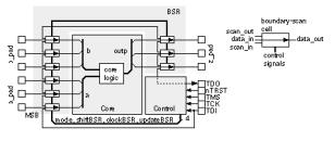
Figure 14.5 shows a boundary-scan register ( BSR ), which consists of a series connection, or chain, of BSCs. The BSR surrounds the ASIC core logic and is connected to the I/O pad cells. The BSR monitors (and optionally controls) the inputs and outputs of an ASIC. The direction of information flow is shown by an arrow on each of the BSCs in
Figure 14.5 . The control signal, mode , is decoded from the IR. Signal mode is drawn as common to all cells for the BSR in Figure 14.5 , but that is not always the case.
entity BSR is
generic (width : INTEGER := 3);
port (shiftDR, clockDR, updateDR, mode, scan_in : BIT;
scan_out : out BIT;
data_in : BIT_VECTOR(width-1 downto 0);
data_out : out BIT_VECTOR(width-1 downto 0));
end BSR;
architecture structure of BSR is
component DR_cell port (
mode, data_in, shiftDR, scan_in, clockDR, updateDR : BIT;
data_out, scan_out : out BIT);
end component ;
for all : DR_cell use entity WORK.DR_cell(behave); signal int_scan : BIT_VECTOR (data_in'RANGE);
begin
BSR : for i in data_in'LOW to data_in'HIGH generate
RIGHT : if (i = 0) generate
BSR_LSB : DR_cell port map (mode, data_in(i), shiftDR,
int_scan(i), clockDR, updateDR, data_out(i), scan_out);
end generate ;
MIDDLE : if ((i > 0) and (i < data_in'HIGH)) generate
BSR_i : DR_cell port map (mode, data_in(i), shiftDR,
int_scan(i), clockDR, updateDR, data_out(i), int_scan(i-1));
end generate ;
LFET : if (i = data_in'HIGH) generate
BSR_MSB : DR_cell port map (mode, data_in(i), shiftDR,
scan_in, clockDR, updateDR, data_out(i), int_scan(i-1));
end generate ;
end generate ;
end structure;
FIGURE 14.5 A BSR (boundary-scan register). An example of the component data-register (DR) cells (used as boundary-scan cells) is shown in Figure 14.2 .
Figure 14.6 shows an instruction register ( IR ), which consists of at least two IR cells connected in series. The IEEE 1149.1 standard specifies that the IR cell is reset to '00...01' (the optional IDCODE instruction). If there is no IDCODE TDR, then the IDCODE instruction defaults to the BYPASS instruction.
entity IR is generic (width : INTEGER := 4); port (
shiftIR, clockIR, updateIR, reset_bar, nTRST, scan_in : BIT; scan_out : out BIT;
data_in : BIT_VECTOR (width-1 downto 0) ;
data_out : out BIT_VECTOR (width-1 downto 0) );
end IR;
architecture structure of IR is
component IR_cell port (shiftIR, data_in, scan_in, clockIR,
updateIR, reset_bar, nTRST, reset_value : BIT ; data_out, scan_out : out BIT );
end component ;
for all : IR_cell use entity WORK.IR_cell(behave); signal int_scan : BIT_VECTOR (data_in'RANGE); signal Vdd : BIT := '1'; signal GND : BIT := '0';
begin
IRGEN : for i in data_in'LOW to data_in'HIGH generate
FIRST : if (i = 0) generate
IR_LSB: IR_cell port map (shiftIR, Vdd, int_scan(i),
clockIR, updateIR, reset_bar, nTRST, Vdd, data_out(i), scan_out); end generate ;
SECOND : if ((i = 1) and (data_in'HIGH > 1)) generate
IR1 : IR_cell port map (shiftIR, GND, int_scan(i),
clockIR, updateIR, reset_bar, nTRST, Vdd, data_out(i), int_scan(i-1)); end generate ;
MIDDLE : if ((i < data_in'HIGH) and (i > 1)) generate
IRi : IR_cell port map (shiftIR, data_in(i), int_scan(i),
clockIR, updateIR, reset_bar, nTRST, Vdd, data_out(i), int_scan(i-1));
end generate ;
LAST : if (i = data_in'HIGH) generate
IR_MSB : IR_cell port map (shiftIR, data_in(i), scan_in,
clockIR, updateIR, reset_bar, nTRST, Vdd, data_out(i), int_scan(i-1)); end generate ; end generate ;
end structure;
FIGURE 14.6 An IR (instruction register).
14.2.3 Instruction Decoder
Table 14.4 shows an instruction decoder . This model is capable of decoding the following minimum set of boundary-scan instructions:
1.EXTEST , external test. Drives a known value onto each output pin to test connections between ASICs.
2.SAMPLE/PRELOAD (often abbreviated to SAMPLE ). Performs two functions: first sampling the present input value from input pad during capture; and then preloading the BSC update register output during update (in preparation for an EXTEST instruction, for example).
3.IDCODE . An optional instruction that allows the device-identification register ( IDCODE) to be shifted out. The IDCODE TDR is an optional register that allows the tester to query the ASIC for the manufacturer s name, part number, and other data that is shifted out on TDO. IDCODE defaults to the BYPASS instruction if there is no IDCODE TDR.
4.BYPASS . Selects the single-cell bypass register (instead of the BSR) and allows data to be quickly shifted between ASICs.
The IEEE 1149.1 standard predefines additional optional instructions and also defines the implementation of custom instructions that may use additional TDRs.
TABLE 14.4 An IR (instruction register) decoder.
entity IR_decoder is generic (width : INTEGER := 4); port (
shiftDR, clockDR, updateDR : BIT; IR_PO : BIT_VECTOR (width-1 downto 0) ;
test_mode, selectBR, shiftBR, clockBR, shiftBSR, clockBSR, updateBSR : out BIT );
end IR_decoder;
architecture behave of IR_decoder is
type INSTRUCTION is (EXTEST, SAMPLE_PRELOAD, IDCODE, BYPASS);
signal I : INSTRUCTION;
begin process (IR_PO) begin case BIT_VECTOR'( IR_PO(1), IR_PO(0) ) is
when "00" => I <= EXTEST; when "01" => I <= SAMPLE_PRELOAD;
when "10" => I <= IDCODE; when "11" => I <= BYPASS;
end case ; end process ;
test_mode <= '1' when I = EXTEST else '0';
selectBR <= '1' when (I = BYPASS or I = IDCODE) else '0'; shiftBR <= shiftDR;
clockBR <= clockDR when (I = BYPASS or I = IDCODE) else '1'; shiftBSR <= shiftDR;
clockBSR <= clockDR when (I = EXTEST or I = SAMPLE_PRELOAD) else '1'; updateBSR <= updateDR when (I = EXTEST or I = SAMPLE_PRELOAD) else '0'; end behave;
14.2.4 TAP Controller
Figure 14.7 shows the TAP controller finite-state machine. The 16-state diagram contains some symmetry: states with suffix '_DR' operate on the data registers and those with suffix '_IR' apply to the instruction register. All transitions between states are determined by the TMS (test mode select) signal and occur at the rising edge of TCK , the boundary-scan clock. An optional active-low reset signal, nTRST or TRST* , resets the state machine to the initial state, Reset . If the dedicated nTRST is not used, there must be a power-on reset signal (POR) not an existing system reset signal.
The outputs of the TAP controller are not shown in Figure 14.7 , but are derived from each TAP controller state. The TAP controller operates rather like a four-button digital watch that cycles through several states (alarm, stopwatch, 12 hr / 24 hr, countdown timer, and so on) as you press the buttons. Only the shaded states in Figure 14.7 affect the ASIC core logic; the other states are intermediate steps. The pause states let the controller jog in place while the tester reloads its memory with a new set of test vectors, for example.
use work.TAP. all ; entity TAP_sm_states is
port (TMS, TCK, nTRST : in BIT; S : out TAP_STATE); end TAP_sm_states;
architecture behave of TAP_sm_states is
type STATE_ARRAY is array (TAP_STATE, 0 to 1) of TAP_STATE; constant T : STATE_ARRAY := ( (Run_Idle, Reset),
(Run_Idle, Select_DR), (Capture_DR, Select_IR), (Shift_DR, Exit1_DR),
(Shift_DR, Exit1_DR), (Pause_DR, Update_DR), (Pause_DR, Exit2_DR),
(Shift_DR, Update_DR), (Run_Idle, Select_DR), (Capture_IR, Reset),
(Shift_IR, Exit1_IR), (Shift_IR, Exit1_IR), (Pause_IR, Update_IR),
(Pause_IR, Exit2_IR), (Shift_IR, Update_IR), (Run_idle, Select_DR) );
begin process (TCK, nTRST) variable S_i: TAP_STATE; begin
if ( nTRST = '0' ) then S_i := Reset;
elsif ( TCK = '1' and TCK'EVENT ) then -- transition on +VE clock edge
if ( TMS = '1' ) then S_i := T(S_i, 1); else S_i := T(S_i, 0); end if ;
end if ; S <= S_i; -- update signal with already updated internal variable
end process ;
end behave;
FIGURE 14.7 The TAP (test-access port) controller state machine.
Table 14.5 shows the output control signals generated by the TAP state machine. I have taken the unusual step of writing separate entities for the state machine and its outputs. Normally this is bad practice because it makes it difficult for synthesis tools to extract and optimize the logic, for example. This separation of functions reflects the fact that the operation of the TAP controller state machine is precisely defined by the IEEE 1149.1 standard independent of the implementation of the register cells and number of instructions supported. The model in Table 14.5 contains the following combinational, registered, and gated output signals and will change with different implementations:
●reset_bar . Resets the IR to IDCODE (or BYPASS in absence of IDCODE TDR).
●selectIR . Connects a register, the IR or a TDR, to TDO .
●enableTDO . Enables the three-state buffer that drives TDO . This allows data to be shifted out of the ASIC on TDO , either from the IR or from the DR, in states shift_IR or shift_DR respectively.
●shiftIR . Selects the serial input to the capture flip-flop in the IR cells.
●clockIR . Causes data at the input of the IR to be captured or the contents of the IR to be shifted toward TDO (depending on shiftIR ) on the negative edge of TCK following the entry to the states shift_IR or capture_IR . This is a dirty signal.
●updateIR . Clocks the update sequential element on the positive edge of TCK at the same time as the exit from state update_IR . This is a dirty signal.
●shiftDR , clockDR , and updateDR . Same functions as corresponding IR signals applied to the TDRs. These signals may be gated to the appropriate TDR by the instruction decoder.
The signals reset_bar , enableTDO , shiftIR , and shiftDR are registered or clocked by TCK (on the positive edge of TCK ). We say these signals are clean (as opposed to being dirty gated clocks).
TABLE 14.5 The TAP (test-access port) control. 1
Reset Run_Idle Select_DR Capture_DR Shift_DR Exit1_DR Pause_DR Exit2_DR Update_DR Select_IR Capture_IR Shift_IR Exit1_IR Pause_IR Exit2_IR Update_IR
reset_bar |
0R |
|
|
|
|
|
|
|
|
selectIR |
1 |
1 |
1 |
1 |
1 |
1 |
1 |
1 |
1 |
enableTDO |
|
|
1R |
|
1R |
|
|
|
|
shiftIR |
|
|
|
|
1R |
|
|
|
|
clockIR |
|
|
|
0G |
0G |
|
|
|
|
updateIR |
|
|
|
|
|
|
|
|
1G |
shiftDR |
|
|
1R |
|
|
|
|
|
|
clockDR |
|
0G |
0G |
|
|
|
|
|
|
updateDR |
|
|
1G |
|
|
|
|
|
|
use work.TAP. all ; entity TAP_sm_output is
port (TCK : in BIT; S : in TAP_STATE; reset_bar, selectIR, enableTDO, shiftIR, clockIR, updateIR, shiftDR, clockDR, updateDR : out BIT);
end TAP_sm_output;
architecture behave_1 of TAP_sm_output is begin -- registered outputs process (TCK) begin if ( (TCK = '0') and TCK'EVENT ) then
if S = Reset then reset_bar <= '0'; else reset_bar <= '1'; end if ;
if S = Shift_IR or S = Shift_DR then enableTDO <= '1'; else enableTDO <= '0'; end if ; if S = Shift_IR then ShiftIR <= '1'; else shiftIR <= '0'; end if ;
if S = Shift_DR then ShiftDR <= '1'; else shiftDR <= '0'; end if ; end if ;
end process ;
process (TCK) begin -- dirty outputs gated with not(TCK) if (TCK = '0' and (S = Capture_IR or S = Shift_IR))
then clockIR <= '0'; else clockIR <= '1'; end if ;
if (TCK = '0' and (S = Capture_DR or S = Shift_DR)) then clockDR <= '0'; else clockDR <= '1'; end if ;
if TCK = '0' and S=Update_IR then updateIR <= '1'; else updateIR <= '0'; end if ;
if TCK = '0' and S=Update_DR then updateDR <= '1'; else updateDR <= '0'; end if ; end process ;
selectIR <= '1' when (S = Reset or S = Run_Idle or S = Capture_IR or S = Shift_IR or S = Exit1_IR or S = Pause_IR or S = Exit2_IR or S = Update_IR) else '0';
end behave_1;
14.2.5 Boundary-Scan Controller
Figure 14.8 shows a boundary-scan controller. It contains the following four parts:
library IEEE; use IEEE.std_logic_1164. all ; use work.TAP. all ;
entity Control is generic (width : INTEGER := 2); port (TMS, TCK, TDI, nTRST : BIT; TDO: out STD_LOGIC; BSR_SO : BIT; BSR_PO : BIT_VECTOR (width-1 downto 0); shiftBSR, clockBSR, updateBSR, test_mode : out BIT); end Control;
architecture mixed of Control is use work.BST_components. all ;
signal reset_bar, selectIR, enableTDO, shiftIR, clockIR, updateIR, shiftDR, clockDR, updateDR, IR_SO, BR_SO, TDO_reg, TDO_data, TDR_SO, selectBR, clockBR, shiftBR : BIT;
signal IR_PI, IR_PO : BIT_VECTOR (1 downto 0); signal S : TAP_STATE;
begin
IR_PI <= "01";
TDO <= TO_STDULOGIC(TDO_reg) when enableTDO = '1' else 'Z';
R1 : process (TCK) begin if (TCK='0') then TDO_reg <= TDO_data; end if ; end process ; TDO_data <= IR_SO when selectIR = '1' else TDR_SO;
TDR_SO <= BR_SO when selectBR = '1' else BSR_SO;
TC1 : TAP_sm_states port map (TMS, TCK, nTRST, S);
TC2 : TAP_sm_output port map (TCK, S, reset_bar, selectIR, enableTDO, shiftIR, clockIR, updateIR, shiftDR, clockDR, updateDR);
IR1 : IR generic map (width => 2) port map (shiftIR, clockIR, updateIR, reset_bar, nTRST, TDI, IR_SO, IR_PI, IR_PO);
DEC1 : IR_decoder generic map (width => 2) port map (shiftDR, clockDR, updateDR, IR_PO, test_mode, selectBR, shiftBR, clockBR, shiftBSR, clockBSR, updateBSR); BR1 : BR_cell port map (clockBR, shiftBR, TDI, BR_SO);
end mixed;
FIGURE 14.8 A boundary-scan controller.
1.Bypass register.
2.TDO output circuit. The data to be shifted out of the ASIC on TDO is selected from the serial outputs of bypass register ( BR_SO ), instruction register ( IR_SO ), or boundary-scan register ( BSR_SO ). Notice the registered output means that data appears on TDO at the negative edge of TCK . This prevents race conditions between ASICs.
3.Instruction register and instruction decoder.
4.TAP controller.
The BSR (and other optional TDRs) are connected to the ASIC core logic outside the BST controller.
14.2.6 A Simple Boundary-Scan Example
Figure 14.9 shows an example of a simple ASIC (our comparator/MUX example) containing boundary scan. The following two packages define the TAP states and the components (these are not essential to understanding what follows, but are included so that the code presented here forms a complete BST model):
entity Core is port (a, b : BIT_VECTOR (2 downto 0); outp : out BIT_VECTOR (2 downto 0)); end Core;
architecture behave of Core is begin outp <= a when a < b else b;
end behave;
library IEEE; use IEEE.std_logic_1164. all ;
entity BST_ASIC is port (TMS, TCK, TDI, nTRST : BIT; TDO : out STD_LOGIC; a_PAD, b_PAD : BIT_VECTOR (2 downto 0); z_PAD : out BIT_VECTOR (2 downto 0)); end BST_ASIC;
architecture structure of BST_ASIC is use work.BST_components. all ; component Core port (a, b: BIT_VECTOR (2 downto 0);
outp: out BIT_VECTOR (2 downto 0)); end component ; for all : Core use entity work.Core(behave);
constant BSR_width : INTEGER := 9;
signal BSR_SO, test_mode, shiftBSR, clockBSR, updateBSR : BIT; signal BSR_PI, BSR_PO : BIT_VECTOR (BSR_width-1 downto 0); signal a, b, z : BIT_VECTOR (2 downto 0);
begin BSR_PI <= a_PAD & b_PAD & z ;
a <= BSR_PO(8 downto 6); b <= BSR_PO(5 downto 3); z_pad <= BSR_PO(2 downto 0); CORE1 : Core port map (a, b, z);
C1 : Control generic map (width => BSR_width) port map (TMS, TCK, TDI, nTRST,
TDO, BSR_SO, BSR_PO, shiftBSR, clockBSR, updateBSR, test_mode);
BSR1 : BSR generic map (width => BSR_width) port map (shiftBSR, clockBSR, updateBSR, test_mode, TDI, BSR_SO, BSR_PI, BSR_PO);
end structure;
FIGURE 14.9 A boundary-scan example. package TAP is
type TAP_STATE is (reset, run_idle, select_DR, capture_DR, shift_DR, exit1_DR, pause_DR, exit2_DR, update_DR, select_IR, capture_IR, shift_IR, exit1_IR, pause_IR, exit2_IR, update_IR); end TAP;
use work.TAP. all ; library IEEE; use IEEE.std_logic_1164. all ; package BST_Components is
component DR_cell port (
mode, data_in, shiftDR, scan_in, clockDR, updateDR: BIT; data_out, scan_out : out BIT );
end component ; component IR_cell port (
shiftIR, data_in, scan_in, clockIR, updateIR, reset_bar, nTRST, reset_value : BIT; data_out, scan_out : out BIT); end component ;
component BR_cell port ( clockDR,shiftDR,scan_in : BIT; scan_out: out BIT );
end component ;
component BSR
generic (width : INTEGER := 5); port (
shiftDR, clockDR, updateDR, mode, scan_in : BIT; scan_out : out BIT;
data_in : BIT_VECTOR(width-1 downto 0); data_out : out BIT_VECTOR(width-1 downto 0)); end component ;
component IR generic (width : INTEGER := 4); port ( shiftIR, clockIR, updateIR, reset_bar, nTRST,
scan_in : BIT; scan_out : out BIT;
data_in : BIT_VECTOR (width-1 downto 0) ; data_out : out BIT_VECTOR (width-1 downto 0) ); end component ;
component IR_decoder generic (width : INTEGER := 4); port ( shiftDR, clockDR, updateDR : BIT;
IR_PO : BIT_VECTOR (width-1 downto 0);
test_mode, selectBR, shiftBR, clockBR, shiftBSR, clockBSR, updateBSR: out BIT );
end component ;
component TAP_sm_states port (
TMS, TCK, nTRST : in BIT; S : out TAP_STATE); end component ; component TAP_sm_output port (
TCK: BIT; S : TAP_STATE; reset_bar, selectIR, enableTDO, shiftIR, clockIR, updateIR, shiftDR, clockDR, updateDR : out BIT);
end component ;
component Control generic (width : INTEGER := 2); port ( TMS, TCK, TDI, nTRST : BIT; TDO : out STD_LOGIC; BSR_SO : BIT; BSR_PO : BIT_VECTOR (width-1 downto 0); shiftBSR, clockBSR, updateBSR, test_mode : out BIT);
end component ;
component BST_ASIC port (
TMS, TCK, TDI : BIT; TDO : out STD_LOGIC; a_PAD, b_PAD : BIT_VECTOR (2 downto 0); z_PAD : out BIT_VECTOR (2 downto 0));
end component ; end ;
The following testbench, Test_BST , performs these functions:
1.Resets the TAP controller at t = 10 ns using nTRST .
2.Continuously clocks the BST clock, TCK , at a frequency of 10 MHz. Rising edges of TCK occur at 100 ns, 200 ns, and so on.
3.Drives a series of values onto the TAP inputs TDI and TMS . The sequence shifts in instruction code‡ '01' (SAMPLE/PRELOAD),‡followed by '00' (EXTEST).
library IEEE; use IEEE.std_logic_1164. all ; library STD; use STD.TEXTIO. all ;
entity Test_BST is end ;
architecture behave of Test_BST is
component BST_ASIC port (TMS, TCK, TDI, nTRST: BIT;
TDO : out STD_LOGIC; a_PAD, b_PAD : BIT_VECTOR (2 downto 0); z_PAD : out BIT_VECTOR (2 downto 0));
end component ;
for all : BST_ASIC use entity work.BST_ASIC(behave);
signal TMS, TCK, TDI, nTRST : BIT; signal TDO : STD_LOGIC; signal TDI_TMS : BIT_VECTOR (1 downto 0);
signal a_PAD, b_PAD, z_PAD : BIT_VECTOR (2 downto 0);
begin
TDI <= TDI_TMS(1) ; TMS <= TDI_TMS(0) ;
ASIC1 : BST_ASIC port map
(TMS, TCK, TDI, nTRST, TDO, a_PAD, b_PAD, z_PAD); nTRST_DRIVE : process begin
nTRST <= '1', '0' after 10 ns, '1' after 20 ns; wait ; PAD_DRIVE : process begin
a_PAD <= ('0', '1', '0'); b_PAD <= ('0', '1', '1'); wait ; end process ;
end process ;
TCK_DRIVE : process begin -- rising edge at 100 ns TCK <= '0' after 50 ns, '1' after 100 ns; wait for 100 ns; if (now > 3000 ns) then wait ; end if ;
end process ;
BST_DRIVE : process begin TDI_TMS <=
--State after +VE edge: ('0', '1') after 0 ns, -- Reset
('0', '0') after 101 ns, -- Run_Idle ('0', '1') after 201 ns, -- Select_DR ('0', '1') after 301 ns, -- Select_IR ('0', '0') after 401 ns, -- Capture_IR ('0', '0') after 501 ns, -- Shift_IR ('1', '0') after 601 ns, -- Shift_IR ('0', '1') after 701 ns, -- Exit1_IR
('0', '1') after 801 ns, -- Update_IR, 01 = SAMPLE/PRELOAD ('0', '1') after 901 ns, -- Select_DR
('0', '0') after 1001 ns, -- Capture_DR ('0', '0') after 1101 ns, -- Shift_DR
--shift 111111101 into BSR, TDI(time) = 101111111 starting now ('1', '0') after 1201 ns, -- Shift_DR
('0', '0') after 1301 ns, -- Shift_DR
('1', '0') after 1401 ns, -- Shift_DR -- shift 4 more 1's ('1', '0') after 1901 ns, -- Shift_DR -- in-between ('1', '1') after 2001 ns, -- Exit1_DR
('0', '1') after 2101 ns, -- Update_DR ('0', '1') after 2201 ns, -- Select_DR ('0', '1') after 2301 ns, -- Select_IR ('0', '0') after 2401 ns, -- Capture_IR ('0', '0') after 2501 ns, -- Shift_IR ('0', '0') after 2601 ns, -- Shift_IR ('0', '1') after 2701 ns, -- Exit1_IR
('0', '1') after 2801 ns, -- Update_IR, 00=EXTEST ('0', '0') after 2901 ns; -- Run_Idle
wait ;
end process ;
process (TDO, a_pad, b_pad, z_pad) variable L : LINE; begin write (L, now, RIGHT, 10); write (L, STRING'(" TDO="));
if TDO = 'Z' then write (L, STRING'("Z")) ; else write (L, TO_BIT(TDO)); end if ;
write (L, STRING'(" PADS=")); write (L, a_pad & b_pad & z_pad); writeline (output, L);
end process ;
end behave;
Here is the output from this testbench:
#0 ns TDO=0 PADS=000000000
#0 ns TDO=Z PADS=010011000
#0 ns TDO=Z PADS=010011010
#650 ns TDO=1 PADS=010011010
#750 ns TDO=0 PADS=010011010

#850 ns TDO=Z PADS=010011010
#1250 ns TDO=0 PADS=010011010
#1350 ns TDO=1 PADS=010011010
#1450 ns TDO=0 PADS=010011010
#1550 ns TDO=1 PADS=010011010
#1750 ns TDO=0 PADS=010011010
#1950 ns TDO=1 PADS=010011010
#2050 ns TDO=0 PADS=010011010
#2150 ns TDO=Z PADS=010011010
#2650 ns TDO=1 PADS=010011010
#2750 ns TDO=0 PADS=010011010
#2850 ns TDO=Z PADS=010011010
#2950 ns TDO=Z PADS=010011101 This trace shows the following activities:
●All changes to TDO and at the pads occur at the negative edge of TCK .
●The core logic output is z_pad = '010' and appears at the I/O pads at t = 0 ns. This is the smaller of the two inputs, a_pad = '010' and b_pad = '011' , and the correct output when the pads are connected to the core logic.
●At t = 650 ns the IDCODE instruction '01' is shifted out on TDO (with '1' appearing first). If we had multiple ASICs in the boundary-scan chain, this would show us that the chain was intact.
●At t = 850 ns the TDO output is floated (to 'Z' ) as we exit the shift_IR state.
●At t = 1200 ns the TAP controller begins shifting the serial data input from TDI ( '111111101' ) into the BSR.
●At t = 1250 ns the BSR data starts shifting out. This is data that was captured during the SAMPLE/PRELOAD instruction from the device input pins, a_pad and b_pad , as well as the driver of the output pins, z_pad . The data appears as the pattern '010011010' . This pattern consists of a_pad = '010' , b_pad = '011' , followed by z_pad = '010' (notice that TDO does not change at t = 1650 ns or 1850 ns).
●At t = 2150 ns, TDO is floated after we exit the shift_DR state.
●At t = 2650 ns the IDCODE instruction '01' (loaded into the IR as we passed through capture_IR the second time) is again shifted out as we shift the EXTEST instruction from TDI into the IR.
●At t = 2650 ns the TDO output is floated after we exit the shift_IR state.
●At t = 2950 ns the output, z_pad , is driven with '101' . The inputs a_pad and b_pad remain unchanged since they are driven from outside the chip. The change on z_pad occurs on the negative edge of TCK because the IR is loaded with the instruction EXTEST on the negative edge of TCK . When this instruction is decoded, the signal mode changes (this signal controls the MUX at the output of the BSCs).
Figure 14.10 shows a signal trace from the MTI simulator for the last four negative edges of TCK . Notice that we shifted in the test pattern on TDI in the order '101111111' . The output z_pad (3 bits wide) is last in the BSR (nearest TDO ) and thus is driven with the first 3 bits of this pattern, '101' . Forcing '101' onto the ASIC output pins would allow us to check that this pattern is correctly received at inputs of other connected ASICs through the bonding wires and board traces. In a later test cycle we can force '010' onto z_pad to check that both logic levels can be transmitted and received. We may also capture other signals (which are similarly being forced onto the outputs of neighboring ASICs) at the inputs.
FIGURE 14.10 Results from the MTI simulator for the boundary-scan testbench.
14.2.7 BSDL
The boundary-scan description language ( BSDL ) is an extension of IEEE 1149.1 but without any overlap. BSDL uses a subset of VHDL. The BSDL for an ASIC is part of an imaginary data sheet; it is not intended for simulation and does not include models for any boundary-scan components. BSDL is a standard way to describe the features and behavior of an ASIC that includes IEEE 1149.1 boundary scan and a standard way to pass information to test-generation software. Using BSDL, test software can also check that the BST features are correct. As an example, test software can use the BSDL to check that the ASIC uses the correct boundary-scan cells for the instructions that claim to be supported. BSDL cannot prove that an implementation works, however.
The following example BSDL description corresponds to our halfgate ASIC example with BST (this code was generated automatically by the Compass tools):
entity asic_p is
generic (PHYSICAL_PIN_MAP : STRING := "DUMMY_PACKAGE");
port (
pad_a: in BIT_VECTOR (0 to 0);
pad_z: buffer BIT_VECTOR (0 to 0);
TCK: in BIT;
TDI: in BIT;
TDO: out BIT;
TMS: in BIT;
TRST: in BIT);
use STD_1149_1_1994. all ;
attribute PIN_MAP of asic_p : entity is PHYSICAL_PIN_MAP;
-- CUSTOMIZE package pin mapping.
constant DUMMY_PACKAGE : PIN_MAP_STRING :=

"pad_a:(1)," & "pad_z:(2)," & "TCK:3," & "TDI:4," & "TDO:5," & "TMS:6," & "TRST:7";
attribute TAP_SCAN_IN of TDI : signal is TRUE; attribute TAP_SCAN_MODE of TMS : signal is TRUE; attribute TAP_SCAN_OUT of TDO : signal is TRUE; attribute TAP_SCAN_RESET of TRST : signal is TRUE; -- CUSTOMIZE TCK max freq and safe stop state.
attribute TAP_SCAN_CLOCK of TCK : signal is (20.0e6, BOTH); attribute INSTRUCTION_LENGTH of asic_p : entity is 3; attribute INSTRUCTION_OPCODE of asic_p : entity is
"IDCODE (001)," & "STCTEST (101)," & "INTEST (100)," & "BYPASS (111)," & "SAMPLE (010)," & "EXTEST (000)";
attribute INSTRUCTION_CAPTURE of asic_p : entity is "001";
--attribute INSTRUCTION_DISABLE of asic_p : entity is " "
--attribute INSTRUCTION_GUARD of asic_p : entity is " "
--attribute INSTRUCTION_PRIVATE of asic_p : entity is " "
attribute IDCODE_REGISTER of asic_p : entity is
"0000" & -- 4-bit version "0000000000000000" & -- 16-bit part number "00000101011" & -- 11-bit manufacturer
"1"; -- mandatory LSB
-- attribute USERCODE_REGISTER of asic_p : entity is " " attribute REGISTER_ACCESS of asic_p : entity is
"BOUNDARY (STCTEST)";
attribute BOUNDARY_CELLS of asic_p : entity is
"BC_1, BC_2";
attribute BOUNDARY_LENGTH of asic_p : entity is 2; attribute BOUNDARY_REGISTER of asic_p : entity is
--num cell port function safe [ccell disval rslt] " 1 ( BC_2, pad_a(0), input, X)," &
" 0 ( BC_1, pad_z(0), output2, X)";
--" 98 ( BC_1, OE, input, X), " &
--" 98 ( BC_1, *, control, 0), " &
--" 99 ( BC_1, myport(0), output3, X, 98, 0, Z);
end asic_p;
The functions of the lines of this BSDL description are as follows:
●Line 2 refers to the ASIC package. We can have the same part (with identical pad numbers on the silicon die) in different ASIC packages. We include the name of the ASIC package in line 2 and the pin mapping between bonding pads and ASIC package pins in lines 14 21 .
●Lines 3 10 describe the signal names of inputs and outputs, the TAP pins, and the optional fifth TAP reset signal. The BST signals do not have to be given the names used in the standard: TCK, TDI, and so on.
●Line 11 refers to the VHDL package, STD_1149_1_1994 . This is a small VHDL package (just over 100 lines) that contains definitions of the constants, types, and attributes used in a BSDL description. It does not contain any models for simulation.
●Lines 22 25 attach signal names to the required TAP pins and the optional fifth TAP reset signal.
● Lines 26 27 refer to the maximum test clock frequency in hertz, and whether the clock may be stopped in both states or just the low state (just the high state is not valid).
●Line 28 describes a 3-bit IR (in the comparator/MUX example we used a 2-bit IR). Length must be greater than or equal to 2.
●Lines 29 35 describe the three required instruction opcodes and mnemonics ( BYPASS, SAMPLE, EXTEST ) and three optional instructions: IDCODE, STCTEST (which is a scan test mode), and INTEST (which supports internal testing in the same fashion as EXTEST supports external testing). EXTEST must be all ones; BYPASS must be all zeros. A mnemonic may have more than one opcode (and opcodes may be specified using 'x' ). Other instructions that may appear here include CLAMP and HIGHZ , both optional instructions that were added to 1149.1 (see Supplement A, 1149.1a). String concatenation is used in BSDL to avoid line-break problems.
●Lines 37 39 include instruction attributes INSTRUCTION_DISABLE (for HIGHZ ), INSTRUCTION_GUARD (for CLAMP ), as well as INSTRUCTION_PRIVATE (for user-defined instructions) that are not used in this example.
●Lines 40 44 describe the IDCODE TDR. The 11-bit manufacturer number is determined from codes assigned by JEDEC Publication 106-A.
●Line 45 describes the USERCODE TDR in a similar fashion to IDCODE, but is not used here.
●Lines 46 47 describe the TDRs for user-defined instructions. In this case the existing BOUNDARY TDR is inserted between TDI and TDO during STCTEST . User-defined

instructions listed here may use the other existing IDCODE and BYPASS TDRs or define new TDRs.
●Lines 48 49 list the boundary-scan cells used in the ASIC. These may be any of the following cells defined in the 1149.1 standard and defined in the VHDL package, STD_1149_1_1994 : BC_1 (Figs. 10-18, 10-29, 10-31c, 10-31d, and 10-33c), BC_2 (Figs. 10-14, 10-30, 10-32c, 10-32d, 10-35c), BC_3 (Fig. 10-15), BC_4 (Figs. 10-16, 10-17), BC_5 (Fig. 10-41c), BC_6 (Fig. 10-34d). The figure numbers in parentheses here refer to the IEEE 1149.1 standard [ IEEE 1149.1b-1994]. Alternatively the cells may be user-defined (and must then be declared in a package).
●Line 50 must be an integer greater than zero and match the number defined by the following register description.
●Lines 51 54 are an array of records, numbered by cell, with seven fields: four required and three that only appear for certain cells. Field 1 specifies the scan cell name as defined in the STD_1149_1_1994 or user-defined package. Field 2 is the port name, with a subscript if the type is BIT_VECTOR . An '*' denotes no connection. Field 3 is one of the following cell functions (with figure or page numbers from the IEEE standard [ IEEE 1149.1b-1994]): input (Fig. 10-18), clock (Fig. 10-17), output2 (two-state output, Fig. 10-29), output3 (three-state, Fig. 10-31d), internal (p. 33, 1149.1b), control (Fig. 10-31c), controlr (Fig. 10-33c), bidir_in (a reversible cell acting as an input, Fig. 10-34d), bidir_out (a reversible cell acting as an output, Fig. 10-34d). Field 4, safe , contains the safe value to be loaded into the update flip-flop when otherwise unspecified, with 'X' as a don t care value.
●Lines 55 57 illustrate the use of the optional three fields. Field 5, ccell or control cell, refers to the cell number (98 in this example) of the cell that controls an output or bidirectional cell. The control cell number 98 is a merged cell in this example with an input cell, input signal name OE , also labeled as cell number 98. The ASIC input OE (for output enable) thus directly controls (enables) the ASIC three-state output, myport(0) .
The boundary-scan standard may seem like a complicated way to test the connections outside an ASIC. However, the IEEE 1149.1 standard also gives us a method to communicate with test circuits inside an ASIC. Next, we turn our attention from problems at the board level to problems that may occur within the ASIC.
1. Outputs: G = gated with TCK, R = registered on falling edge of TCK. Only active levels are shown in the table.