

14.8 A Simple Test Example
As an example, we will describe automatic test generation using boundary scan together with internal scan. We shall use the function Z = A'B + BC for the core logic and register the three inputs using three flip-flops. We shall test the resulting sequential logic using a scan chain. The simple logic will allow us to see how the test vectors are generated.
14.8.1 Test-Logic Insertion
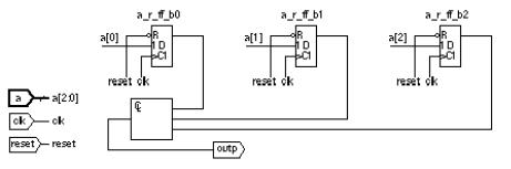
Figure 14.31 shows a structural Verilog model of the logic core. The three flip-flops (cell name dfctnb ) implement the input register. The combinational logic implements the function, outp = a_r[0]'.a_r[1] + a_r[1].a_r[2 ]. This is the same function as Figure 14.14 and Figure 14.16 .
module core_p (outp, reset, a, clk);
output outp; input reset, clk; input [2:0] a; wire [2:0] a_r;
dfctnb a_r_ff_b0 (.D(a[0]), .CP(clk), .CDN(reset), .Q(a_r[0]), .QN(\a_r_ff_b0.QN )); dfctnb a_r_ff_b1 (.D(a[1]), .CP(clk), .CDN(reset), .Q(a_r[1]), .QN(\a_r_ff_b1.QN )); dfctnb a_r_ff_b2 (.D(a[2]), .CP(clk), .CDN(reset), .Q(a_r[2]), .QN(\a_r_ff_b2.QN )); in01d0 u2 (.I(a_r[0]), .ZN(u2_ZN));
nd02d0 u3 (.A1(u2_ZN), .A2(a_r[1]), .ZN(u3_ZN)); nd02d0 u4 (.A1(a_r[1]), .A2(a_r[2]), .ZN(u4_ZN)); nd02d0 u5 (.A1(u3_ZN), .A2(u4_ZN), .ZN(outp));
endmodule
FIGURE 14.31 Core of the Threegates ASIC.
Table 14.15 shows the structural Verilog for the top-level logic of the Threegates ASIC including the I/O pads. There are nine pad cells. Three instances (up1_b0 , up1_b1 , and up1_b2 ) are the data-input pads, and one instance, up2_1 , is the output pad. These were vectorized pads (even for the output that had a range of 1), so the synthesizer has added suffixes ( '_1' and so on) to the pad instance names. Two pads are for power, one each for ground and the positive supply, instances up11 and up12 . One pad, instance up3_1 , is for the reset signal. There are two pad cells for the clock. Instance up4_1 is the clock input pad attached to the package pin and instance up6 is the clock input buffer.
The next step is to insert the boundary-scan logic and the internal-scan logic. Some synthesis tools can create test logic as they synthesize, but for most tools we need to perform test-logic insertion as a separate step. Normally we complete a parameter sheet specifying the type of test logic (boundary scan with internal scan in this case), as well as the ordering of the scan chain. In our example, we shall include all of the sequential cells in the boundary-scan register and order the boundary-scan cells using the pad numbers (in the original behavioral
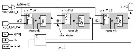
input). Figure 14.32 shows the modified core logic. The test software has changed all the flip-flops (cell names dfctnb ) to scan flip-flops (with the same instance names, but the cell names are changed to mfctnb ). The test software also adds a noninverting buffer to drive the scan-select signal to all the scan flip-flops.
The test software also adds logic to the top level. We do not need a detailed understanding of the automatically generated logic, but later in the design flow we will need to understand what has been done. Figure 14.33 shows a high-level view of the Threegates ASIC before and after test-logic insertion.
TABLE 14.15 The top level of the Threegates ASIC before test-logic insertion. module asic_p (pad_outp, pad_a, pad_reset, pad_clk);
output [0:0] pad_outp; input [2:0] pad_a; input [0:0] pad_reset, pad_clk;
wire [0:0] reset_sv, clk_sv, outp_sv; wire [2:0] a_sv; supply1 VDD; supply0 VSS;
core_p uc1 (.outp(outp_sv[0]), .reset(reset_sv[0]), .a(a_sv[2:0]), .clk(clk_bit));
pc3o07 up2_1 (.PAD(pad_outp[0]), .I(outp_sv[0]));
pc3c01 up6 (.CCLK(clk_sv[0]), .CP(clk_bit));
pc3d01r up3_1 (.PAD(pad_reset[0]), .CIN(reset_sv[0]));
pc3d01r up4_1 (.PAD(pad_clk[0]), .CIN(clk_sv[0]));
pc3d01r up1_b0 (.PAD(pad_a[0]), .CIN(a_sv[0])); pc3d01r up1_b1 (.PAD(pad_a[1]), .CIN(a_sv[1])); pc3d01r up1_b2 (.PAD(pad_a[2]), .CIN(a_sv[2]));
pv0f up11 (.VSS(VSS));
pvdf up12 (.VDD(VDD));
endmodule
module core_p_ta (a_r_2, outp, a_r_ff_b0_DA, taDriver12_I, a, clk, reset); output a_r_2, outp; input a_r_ff_b0_DA, taDriver12_I;
input [2:0] a; input clk, reset; wire [1:0] a_r; supply1 VDD; supply0 VSS; ni01d5 taDriver12 (.I(taDriver12_I), .Z(taDriver12_Z));
mfctnb a_r_ff_b0 (.DA(a_r_ff_b0_DA), .DB(a[0]), .SA(taDriver12_Z), .CP(clk),
.CDN(reset), .Q(a_r[0]), .QN(\a_r_ff_b0.QN ));
mfctnb a_r_ff_b1 (.DA(a_r[0]), .DB(a[1]), .SA(taDriver12_Z), .CP(clk), .CDN(reset),
.Q(a_r[1]), .QN(\a_r_ff_b1.QN ));
mfctnb a_r_ff_b2 (.DA(a_r[1]), .DB(a[2]), .SA(taDriver12_Z), .CP(clk), .CDN(reset),
.Q(a_r_2), .QN(\a_r_ff_b2.QN )); in01d0 u2 (.I(a_r[0]), .ZN(u2_ZN));

nd02d0 u3 (.A1(u2_ZN), .A2(a_r[1]), .ZN(u3_ZN)); nd02d0 u4 (.A1(a_r[1]), .A2(a_r_2), .ZN(u4_ZN)); nd02d0 u5 (.A1(u3_ZN), .A2(u4_ZN), .ZN(outp));
endmodule
FIGURE 14.32 The core of the Threegates ASIC after test-logic insertion.
FIGURE 14.33 The Threegates ASIC. (a) Before test-logic insertion. (b) After test-logic insertion.
14.8.2 How the Test Software Works
The structural Verilog for the Threegates ASIC is lengthy, so Figure 14.34 shows only the essential parts. The following main blocks are labeled in Figure 14.34 :
1.This block is the logic core shown in Figure 14.32 . The Verilog module header shows the local andformal port names. Arrows indicate whether each signal is an input or an output.
2.This is the main body of logic added by the test software. It includes the boundary-scan controller and clock control.
3.This block groups together the buffers that the test software has added at the top level to drive the control signals throughout the boundary-scan logic.
4.This block is the first boundary-scan cell in the BSR. There are six boundary-scan cells: three input cells for the data inputs, one output cell for the data output, one input cell for the reset, and one input cell for the clock. Only the first (the boundary-scan input cell for a[0] ) and the last boundary-scan cells are shown. The others are similar.
5.This is the last boundary-scan cell in the BSR, the output cell for the clock.
6.This is the clock pad (with input connected to the ASIC package pin). The cell itself is unchanged by the test software, but the connections have been altered.
7.This is the clock-buffer cell that has not been changed.
8.The test software adds five I/O pads for the TAP. Four are input pad cells for TCK, TMS, TDO, and TRST. One is a three-state output pad cell for TDO.
9.The power pad cells remain unchanged.
10.The remaining I/O pad cells for the three data inputs, the data output, and reset remain unchanged, but the connections to the core logic are broken and the boundary-scan cells inserted.
The numbers in Figure 14.34 link the signals in each block to the following explanations:
1.The control signals for the input BSCs are C_0, C_1, C_2, and C_4 and these are all buffered, together with the test clock TCK . The single output BSC also requires the control signal C_3 and this is driven from the BST controller.

2.The clock enters the ASIC package through the clock pad as .PAD(clk[0]) and exits the clock pad cell as
.CIN(up_4_1_CIN1) . The test software routes this to the data input of the last boundary-scan cell as
.PI(up_4_1_CIN1) and the clock exits as .PO(up_4_1_cin) . The clock then passes through the clock buffer, as before.
3.The serial input of the first boundary-scan cell comes from the controller as
.bst_control_BST_SI(test_logic_bst_control_BST_SI) .
4.The serial output of the last boundary-scan cell goes to the controller as .bst_control_BST(up4_1_bst_SO)
.
5.The beginning of the BSR is the first scan flip-flop in the core, which is connected to the TDI input as
.a_r_ff_b0_DA(ta_TDI_CIN) .
6.The end of the scan chain leaves the core as .a_r_2(uc1_a_r_2) and enters the controller as
.bst_control_scan_SO(uc1_a_r_2) .
7.The scan-enable signal .bst_control_C_9(test_logic_bst_control_C_9) is generated by the boundary-scan controller, and connects to the core as .taDriver12_I(test_logic_bst_control_C_9) .
FIGURE 14.34 The top level of the Threegates ASIC after test-logic insertion.
The added test logic is shown in Figure 14.35 . The blocks are as follows:
1.This is the module declaration for the test logic in the rest of the diagram, it corresponds to block B in Table 14.34 .
2.This block contains buffers and clock control logic.
3.This is the boundary-scan controller.
4.This is the first of 26 IDR cells. In this implementation the IDCODE register is combined with the BSR. Since there are only six BSR cells we need (32 6) or 26 IDR cells to complete the 32-bit IDR.
5.This is the last IDR cell.
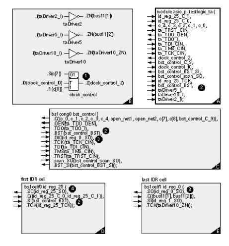
FIGURE 14.35 |
Test logic inserted in the Threegate ASIC. |
|
|
|
|
|
|
|
|||||||
TABLE 14.16 |
The TAP (test-access port) control. 1 |
|
|
|
|
|
|
|
|||||||
|
|
|
|
|
|
|
|
|
|
|
C_8 2 |
C_9 |
|||
TAP state |
C_0 |
C_1 |
C_2 |
C_3 |
C_4 |
C_5 |
C_6 |
C_7 |
|||||||
|
|
|
|
|
|
|
|||||||||
Reset |
x |
|
x |
xxxx0xx xxxx0xx xxxx0xx xxxx0xx xxxx1xx xxxx0xx xxxx0xx xxxx0xx |
|||||||||||
Run_Idle |
00x0xxx |
11x1xxx |
0 |
1001011 0001011 |
0000010 |
1 |
0000001 |
0000000 |
0000000 |
||||||
Select_DR |
00x0xxx |
11x1xxx |
0 |
1001011 0001011 |
0000010 |
1 |
0000001 |
0000000 |
0000000 |
||||||
Capture_DR 00x01xx |
00x00xx |
0 |
1001011 0001011 |
0000010 |
1 |
0000001 |
000000T |
0000000 |
|||||||
Shift_DR |
11x11xx |
11x11xx |
0 |
1001011 0001011 |
0000010 |
1111101 |
0000001 |
000000T |
0000001 |
||||||
Exit1_DR |
00x00xx |
11x11xx |
0 |
1001011 0001011 |
0000010 |
1 |
0000001 |
0000000 |
0000000 |
||||||
Pause_DR |
00x00xx |
11x11xx |
0 |
1001011 0001011 |
0000010 |
1 |
0000001 |
0000000 |
0000000 |
||||||
Exit2_DR |
00x00xx |
11x11xx |
0 |
1001011 0001011 |
0000010 |
1 |
0000001 |
0000000 |
0000000 |
||||||
Update_DR |
00x0xxx |
11x1xxx |
110100 |
1001011 0001011 |
0 |
1111101 |
0000001 |
0000000 |
0000000 |
||||||
Select_IR |
x |
|
x |
0 |
1001011 0001011 |
00000x0 |
11111x1 |
0000001 |
0000000 |
0000000 |
|||||
Capture_IR |
x |
|
x |
0 |
1001011 0001011 |
00000x0 |
11111x1 |
0000001 |
0000000 |
0000000 |
|||||
Shift_IR |
x |
|
x |
0 |
1001011 0001011 |
00000x0 |
11111x1 |
0000001 |
0000000 |
0000000 |
|||||
Exit1_IR |
x |
|
x |
0 |
1001011 0001011 |
00000x0 |
11111x1 |
0000001 |
0000000 |
0000000 |
|||||
Pause_IR |
x |
|
x |
0 |
1001011 0001011 |
00000x0 |
11111x1 |
0000001 |
0000000 |
0000000 |
|||||
Exit2_IR |
x |
|
x |
0 |
1001011 0001011 |
00000x0 |
11111x1 |
0000001 |
0000000 |
0000000 |
|||||
Update_IR |
x |
|
x |
0 |
1001011 0001011 |
00000x0 |
1111101 |
0000001 |
0000000 |
0000000 |
|||||
The numbers in Figure 14.35 refer to the following explanations:
1.The system clock (CLK, not the test clock TCK) from the top level (after passing through the boundary-scan cell) is fed through a MUX so that CLK may be controlled during scan.
2.The signal bst_control_BST is the end (output) of the boundary-scan cells and the start (input) to the ID register only cells.
3.The signal id_reg_0_SO is the end (output) of the ID register.
4.The signal bst_control_BST_SI is the start of the boundary-scan chain.
The job of the boundary-scan controller is to produce the control signals ( C_1 through C_9 ) for each of the 16 TAP controller states ( reset through update_IR ) for each different instruction. In this BST implementation there are seven instructions: the required EXTEST , SAMPLE , and BYPASS ; IDCODE ; INTEST (which is the equivalent of EXTEST , but for internal test); RUNBIST (which allows on-chip test structures to operate); and SCANM (which controls the internal-scan chains). The boundary-scan controller outputs are shown in Table 14.16 .
There are two very important differences between this controller and the one described in Table 14.5 . The first, and most obvious, is that the control signals now depend on the instruction. This is primarily because INTEST requires the control signal at the output of the BSCs to be in different states for the input and output cells. The second difference is that the logic for the boundary-scan cell control signals is now purely combinational we have removed the gated clocks. For example, Figure 14.36 shows the input boundary-scan cell. The clock for the shift flip-flop is now TCK and not a gated clock as it was in Table 14.5 . We can do this because the output of the flip-flop, SO , the scan output, is added as input to the MUX that feeds the flip-flop data input. Thus, when we wish to hold the state of the flip-flop, the control signals select SO to be connected from the output to the input. This is called a polarity-hold flip-flop . Unfortunately, we have little choice but to gate the system clock if we make the scan chain part of the BSR. We cannot have one clock for part of the BSR and another for the rest. The costly alternative is to change every scan flip-flop to a scanned polarity-hold flip-flop.
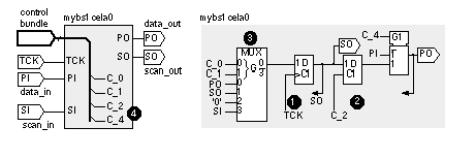
module mybs1cela0 (SO, PO, C_0, TCK, SI, C_1, C_2, C_4, PI);
output SO, PO; input C_0, C_1, C_2, C_4, TCK, SI, PI;
in01d1 inv_0 (.I(C_0), .ZN(iv0_ZN));
in01d1 inv_1 (.I(C_1), .ZN(iv1_ZN));
oa03d1 oai221_1 (.A1(C_0), .A2(SO), .B1(iv0_ZN), .B2(SI), .C(C_1), .ZN(oa1_ZN));
nd02d1 nand2_1 (.A1(na2_ZN), .A2(oa1_ZN), .ZN(na1_ZN));
nd03d1 nand3_1 (.A1(PO), .A2(iv0_ZN), .A3(iv1_ZN), .ZN(na2_ZN));
mx21d1 mux21_1 (.I0(PI), .I1(upo), .S(C_4), .Z(PO));
dfntnb dff_1 (.D(na1_ZN), .CP(TCK), .Q(SO), .QN(\so.QN ));
lantnb latch_1 (.E(C_2), .D(SO), .Q(upo), .QN(\upo.QN ));
endmodule
FIGURE 14.36 Input boundary-scan cell (BSC) for the Threegates ASIC. Compare this to the generic data-register (DR) cell (used as a BSC) shown in Figure 14.2 .
14.8.3 ATVG and Fault Simulation
Table 14.17 shows the results of running the Compass ATVG software on the Threegates ASIC. We might ask: Why so many faults? and why is the fault coverage so poor? First we look at the details of the test software output. We notice the following:
● Line 2 . The backtrace limit is 30. We do not have any deep complex combinational logic so that this

should not cause a problem.
●Lines 4 6 . An uncollapsed fault count of 184 indicates the test software has inserted faults on approximately 100 nodes, or at most 50 gates assuming a fanout of 1, less gates with any realistic fanout. Clearly this is less than all of the test logic that we have inserted.
TABLE 14.17 ATVG (automatic test-vector generation) report for the Threegates ASIC. CREATE: Output vector database cell defaulted to [svf]asic_p_ta
CREATE: Backtrack limit defaulted to 30
CREATE: Minimal compression effort: 10 (default)
Fault list generation/collapsing
Total number of faults: 184
Number of faults in collapsed fault list: 80
Vector generation
#
#VECTORS FAULTS FAULT COVER
#processed
#
#5 184 60.54%
#Total number of backtracks: 0
#Highest backtrack : 0
#Total number of vectors : 5
#
#STAR RESULTS summary
#Noncollapsed Collapsed
#Fault counts:
#Aborted 0 0
#Detected 89 43
#Untested 58 20
#------ ------
#Total of detectable 147 63
#Redundant 6 2
#Tied 31 15
#
#FAULT COVERAGE 60.54 % 68.25 %
#Fault coverage = nb of detected faults / nb of detectable faults Vector/fault list database [svf]asic_p_ta created.
To discover why the fault coverage is 68.25 percent we must examine each of the fault categories. First,
Table 14.18 shows the undetected faults.
TABLE 14.18 Untested faults (not observable) for the Threegates ASIC.
Faults |
Explanation |
|
TADRIVER4.ZN sa0 |
Internal driver for BST control bundle (seven more faults like this). |
|
TA_TRST.1.CIN sa0 |
||
BST reset TRST is active-low and tied high during test. |
||
TDI.O sa0 sa1 |
||
TDI is BST serial input. |
||
|
UP1_B0.1.CIN sa0 sa1
Data input pad (two more faults like this one).
UP3_1.1.CIN sa0
System reset is active-low and tied high during test.
UP4_1.1.CIN sa0 sa1
System clock input pad.
# Total number: 20
The ATVG program is generating tests for the core using internal scan. We cannot test the BST logic itself, for example. During the production test we shall test the BST logic first, separately from the core this is often called a flush test . Thus we can ignore any faults from the BST logic for the purposes of internal-scan testing.
Next we find two redundant faults: TA_TDO.1.I sa0 and sa1 . Since TDO is three-stated during the test, it makes no difference to the function of the logic if this node is tied high or low hence these faults are redundant. Again we should ensure these faults will be caught during the flush test. Finally, Table 14.19 shows the tied faults.
TABLE 14.19 Tied faults. |
|
|
Fault(s) |
Explanation |
|
TADRIVER1.ZN sa0 |
Internal BST buffer (seven more faults like this one). |
|
TA_TMS.1.CIN sa0 |
||
TMS input tied low. |
||
TA_TRST.1.CIN sa1 |
||
TRST input tied high. |
||
|
TEST_LOGIC.BST_CONTROL.U1.ZN sa1
Internal BST logic.
UP1_B0_BST.U1.A2 sa0
Input pad (two more faults like this).
UP3_1.1.CIN sa1
Reset input pad tied high.
# Total number: 15
Now that we can explain all of the undetectable faults, we examine the detected faults. Table 14.20 shows only the detected faults in the core logic. Faults F1 F8 in the first part of Table 14.20 correspond to the faults in Figure 14.16 . The fault list in the second part of Table 14.20 shows each fault in the core and whether it was detected (D) or collapsed and detected as an equivalent fault (CD). There are no undetected faults (U) in the logic core.
TABLE 14.20 Detected core-logic faults in the Threegates ASIC.
Fault(s) |
Explanation |
UC1.U2.ZN sa1 |
F1 |
UC1.U3.A2 sa1 |
F2 |
UC1.U3.ZN sa1 |
F5 |
UC1.U4.A1 sa1 |
F3 |
UC1.U4.ZN sa1 |
F6 |
UC1.U5.ZN sa0 |
F8 |
UC1.U5.ZN sa1 |
F7 |
UC1.A_R_FF_B2.Q.O sa1 |
F4 |
Fault list |
|
UC1.A_R_FF_B0.Q: (O) CD CD |
SA0 and SA1 collapsed to U3.A1 |
UC1.A_R_FF_B1.Q: (O) D D |
SA0 and SA1 detected. |
UC1.A_R_FF_B2.Q: (O) CD D |
SA0 collapsed to U2. SA1 is F4. |
UC1.U2: (I) CD CD (ZN) CD D |
I.SA1/0 collapsed to O.SA1/0. O. SA1 is F1. |
UC1.U3: (A1) CD CD (A2) CD D (ZN) CD D A1.SA1 collapsed to U2.ZN.SA1.
UC1.U4: (A1) CD D (A2) CD CD (ZN) CD D A2.SA1 collapsed to A_R_FF_B2.Q.SA1.
UC1.U5: (A1) CD CD (A2) CD CD (ZN) D D A1.SA1 collapsed to U3.ZN.SA1
14.8.4 Test Vectors
Next we generate the test vectors for the Threegates ASIC. There are three types of vectors in scan testing. Serial vectors are the bit patterns that we shift into the scan chain. We have three flip-flops in the scan chain plus six boundary-scan cells, so each serial vector is 9 bits long. There are serial input vectors that we apply as a stimulus and serial output vectors that we expect as a response. Parallel vectors are applied to the pads before we shift the serial vectors into the scan chain. We have nine input pads (three core data, one core clock, one core reset, and four input TAP pads TMS , TCK , TRST , and TDI ) and two outputs (one core data output and TDO ). Each parallel vector is thus 11 bits long and contains 9 bits of stimulus and 2 bits of response. A test program consists of applying the stimulus bits from one parallel vector to the nine input pins for one test cycle. In the next nine test cycles we shift a 9-bit stimulus from a serial vector into the scan chain (and receive a 9-bit response, the result of the previous tests, from the scan chain). We can generate the serial and parallel vectors separately, or we can merge the vectors to give a set of broadside vectors . Each broadside vector corresponds to one test cycle and can be used for simulation. Some testers require broadside vectors; others can generate them from the serial and parallel vectors.
TABLE 14.21 Serial test vectors
Serial-input scan data
#1 1 |
1 |
1 |
0 |
1 |
0 |
1 |
1 |
0 |
#2 1 |
0 |
1 |
1 |
0 |
1 |
0 |
0 |
1 |
#3 1 |
1 |
0 |
1 |
1 |
1 |
0 |
1 |
0 |
#4 0 |
0 |
0 |
1 |
0 |
0 |
0 |
0 |
0 |
#5 0 |
1 |
0 |
0 |
1 |
1 |
1 |
0 |
1 |
^UC1.A_R_FF_B0.Q ^UP1_B2_BST.SO.Q ^UP2_1_BST.SO.Q
^UC1.A_R_FF_B1.Q ^UP1_B1_BST.SO.Q ^UP3_1_BST.SO.Q
^UC1.A_R_FF_B2.Q ^UP1_B0_BST.SO.Q ^UP4_1_BST.SO.Q
Fault |
Fault number |
Vector number |
Core input |
UC1.U2.ZN sa1 |
F1 |
3 |
011 |
UC1.U3.A2 sa1 |
F2 |
4 |
000 |
UC1.U3.ZN sa1 |
F5 |
5 |
010 |
UC1.U4.A1 sa1 |
F3 |
2 |
101 |
UC1.U4.ZN sa1 |
F6 |
1 |
111 |
UC1.U5.ZN sa0 |
F8 |
1 |
111 |
UC1.U5.ZN sa1 |
F7 |
2 |
101 |
UC1.A_R_FF_B2.Q.O sa1 |
F4 |
2 |
101 |
Table 14.21 shows the serial test vectors for the Threegates ASIC. The third serial test vector is '110111010' . This test vector is shifted into the BSR, so that the first three bits in this vector end up in the first three bits of the BSR. The first three bits of the BSR, nearest TDI , are the scan flip-flops, the other six bits are boundary-scan cells). Since UC1.A_R_FF_B0.Q is a_r[0] and so on, the third test vector will set a_r = 011 where a_r[2] = 0. This is the vector we require to test the function a_r[0]'.a_r[1] + a_r[1].a_r[2 ] for fault UC1.U2.ZN sa1 in the Threegates ASIC. From Figure 14.31 we see that this is a stuck-at-1 fault on the output of the inverter whose input is connected to a_r[0] . This fault corresponds to fault F1 in the circuit of Figure 14.16 . The fault simulation we performed earlier told us the vector ABC = 011 is a test for fault F1 for the function A'B + BC.
14.8.5 Production Tester Vector Formats
The final step in test-program generation is to format the test vectors for the production tester. As an example the following shows the Sentry tester file format for testing a D flip-flop. For an average ASIC there would be thousands of vectors in this file.
#Pin declaration: pin names are separated by semi-colons (all pins
#on a bus must be listed and separated by commas)
pre_; clr_; d; clk; q; q_;
#Pin declarations are separated from test vectors by $
$
#The first number on each line is the time since start in ns,
#followed by space or a tab.
#The symbols following the time are the test vectors
#(in the same order as the pin declaration)
#an "=" means don't do anything
#an "s" means sense the pin at the beginning of this time point
#(before the input changes at this time point have any effect)
#pcdcqq
#rlal _
#ertk
#__a
00 1010== # clear the flip-flop
10 1110ss # d=1, clock=0
20 1111ss # d=1, clock=1
30 1110ss # d=1, clock=0
40 1100ss # d=0, clock=0
50 1101ss # d=0, clock=1
60 1100ss # d=0, clock=0
70 ====ss
14.8.6 Test Flow
Normally we leave test-vector generation and the production-test program generation until the very last step in ASIC design after physical design is complete. All of the steps have been described before the discussion of physical design, because it is still important to consider test very early in the design flow. Next, as an example of considering test as part of logical design, we shall return to our Viterbi decoder example.
TABLE 14.22 Timing effects of test-logic insertion for the Viterbi decoder.
Timing of critical paths before test-logic insertion
#Slack(ns) Num Paths
#-3.3826 1 *
#-1.7536 18 *******
#-.1245 4 **
#1.5045 1 *
#3.1336 0 *
#4.7626 0 *
#6.3916 134 ******************************************
#8.0207 6 ***
#9.6497 3 **
#11.2787 0 *
#12.9078 24 ********
#instance name
#inPin --> outPin incr arrival trs rampDel cap cell
#(ns) (ns) (ns) (pf)
#v_1.u100.u1.subout6.Q_ff_b0
#CP --> QN 1.73 1.73 R .20 .10 dfctnb
...
#v_1.u100.u2.metric0.Q_ff_b4
#setup: D --> CP .16 21.75 F .00 .00 dfctnh
After test-logic insertion
#-4.0034 1 *
#-1.9835 18 *****
#.0365 4 **
#2.0565 1 *
#4.0764 0 *
#6.0964 138 *******************************
#8.1164 2 *
#10.1363 3 **
#12.1563 24 ******

#14.1763 0 *
#16.1963 187 ******************************************
#v_1.u100.u1.subout7.Q_ff_b1
#CP --> Q 1.40 1.40 R .28 .13 mfctnb
...
#v_1.u100.u2.metric0.Q_ff_b4
#setup: DB --> CP .39 21.98 F .00 .00 mfctnh
1.Outputs are specified for each instruction as 0123456, where: 0 = EXTEST, 1 = SAMPLE, 2 = BYPASS, 3 = INTEST, 4 = IDCODE, 5 = RUNBIST, 6 = SCANM.
2.T denotes gated clock TCK.
14.9 The Viterbi Decoder
Example
Table 14.22 shows the timing analysis for the Viterbi decoder before and after test insertion. The Compass test software inserts internal scan and boundary scan exactly as in the Threegates example. The timing analysis is in the form of histograms showing the distributions of the timing delays for all paths. In this analysis we set an aggressive constraint of 20 ns (50 MHz) for the clock. The critical path before test insertion is 21.75 ns (the slack is thus negative at 1.75 ns). The path starts at u1.subout6.Q_ff_b0 and ends at u2.metric0.Q_ff_b4 , both flip-flops inside the flattened block, v_1.u100 , that we created during synthesis in an attempt to improve speed. The first flip-flop in the path is a dfctnb ; the last flip-flop is a dfctnh . The suffix 'b' denotes 1X drive and suffix 'h' denotes 2X drive.
After test insertion the critical path is 21.98 ns. The end point is identical, but the start point is now subout7.Q_ff_b1 . This is not too surprising. What is happening is that there are a set of paths of nearly equal length. Changing the flip-flops to their scan versions ( mfctnb and mfctnh ) increases the delay slightly. The exact delay depends on the capacitive load at the output, the path (clock-to-Q, clock-to-QN, or setup), and the input signal rise time.
Adding test logic has not increased the critical path delay substantially. Almost as important is that the distribution of delays has not changed substantially. Also very important is the fact that the distributions show that there are only approximately 20 paths with delays close to the critical path delay. This means that we should be able to constrain these paths during physical design and achieve a performance after routing that is close to our preroute predictions.
TABLE 14.23 Fault coverage for the Viterbi decoder.
Fault list generation/collapsing
Total number of faults: 8846
Number of faults in collapsed fault list: 3869 Vector generation
#
#VECTORS FAULTS FAULT COVER
#processed
#
#20 7515 82.92%
#40 8087 89.39%
#60 8313 91.74%
#80 8632 95.29%
#87 8846 96.06%
#Total number of backtracks: 3000
#Highest backtrack : 30
#Total number of vectors : 87
#STAR RESULTS summary
#Noncollapsed Collapsed
#Fault counts:
#Aborted 178 85
#Detected 8427 3680
#Untested 168 60
#------ ------
#Total of detectable 8773 3825
#
# Redundant 10 6

#Tied 63 38
#FAULT COVERAGE 96.06 % 96.21 %
Next we check the logic for fault coverage. Table 14.23 shows that the ATPG software has inserted nearly 9000 faults, which is reasonable for the size of our design. Fault coverage is 96 percent. Most of the untested and tied faults arise from the BST logic exactly as we have already described in the Threegates example. If we had not completed this small test case first, we might not have noticed this. The aborted faults are almost all within the large flattened block, v_1.u100 . If we assume the approximately 60 faults due to the BST logic are covered by a flush test, our fault coverage increases to 3740/3825 or 98 percent. To improve upon this figure, some, but not all, of the aborted faults can be detected by substantially increasing the backtrack limit from the default value of 30. To discover the reasons for the remaining aborted faults, we could use a controllability/observability program. If we wish to increase the fault coverage even further, we either need to change our test approach or change the design architecture. In our case we believe that we can probably obtain close to 99 percent stuck-at fault coverage with the existing architecture and thus we are ready to move on to physical design.