

8.7 References
Page numbers in brackets after a reference indicate its location in the chapter body.
Actel. 1996. FPGA Data Book and Design Guide. No catalog information. Available from Actel Corporation, 955 East Arques Avenue, Sunnyvale, CA 94086-4533, (408) 739-1010. Contains design guides and applications notes, including: Estimating Capacity and Performance for ACT 2 FPGA Designs (describes circuits to connect FPGAs to PALs); Binning Circuit of Actel FPGAs (describes circuits and data for performance measurement); Global Clock Networks (describes clock distribution schemes); Fast On and Off Chip Delays with ACT 2 I/O Latches (describes techniques to improve I/O performance); Board Level Considerations for Actel FPGAs (describes ground bounce and SSO problems); A Power-On Reset (POR) Circuit for Actel Devices (describes problems caused by slowly rising supply voltage); Implementing Load ( sic ) Latency Fast Counters with ACT 2 FPGAs; Oscillators for Actel FPGAs (describes crystal and RC oscillators); Designing a DRAM Controller Using Language-Based Synthesis (a detailed Verilog description of a 4 MB DRAM controller including refresh). See also the Actel Web site. [ reference location ]
Altera. 1996. Data Book. No catalog information. Available from Altera Corporation, 2610 Orchard Parkway, San Jose, CA 95134-2020, (408) 944-0952. Contains information on the FLEX 10k and 8000 complex PLDs; MAX 9000, 7000, and 5000 complex PLDs; FLASHlogic; and EPLDs. A limited number of application notes are also included. More information may be found at the Altera Web site. [ reference location ]
Connor, D. 1992. Taking the first steps. EDN, April 9, p. 98. ISSN 0012-7515. The second part of this article, Migrating to FPGAs: Any designer can do it, wa published in EDN, April 23, 1992, p. 120. See also http://www.ednmag.com .
Both articles are reprinted in the 1994 Actel Data Book. A description of designing, simulating, and testing a voicemail system using Viewlogic software. [ reference location ]
Skahill, K. 1996. VHDL for Programmable Logic. Menlo Park, CA: Addison-Wesley, 593 p. ISBN 0-201-89573-0. TK7885.7.S55. Covers VHDL design for PLDs using Cypress Warp design system. [ reference location ]
Xilinx. 1996. The Programmable Logic Data Book. No catalog information. Available from Xilinx Corporation, 2100 Logic Drive, San Jose, CA 95124-3400,
(408) 559-7778. Contains details of XC9500, XC7300, and XC7200 CPLDs; XC5200, XC4000, XC3000 LCA FPGAs; and XC6200 sea-of-gates FPGAs. Earlier editions of this data book (the 1994 edition, for example) contained a section titled Best of XCELL that contained extremely useful design information. Much of this design material is now only available online, at the Xilinx Web site. [ reference location ]
9.1 Schematic Entry
Schematic entry is the most common method of design entry for ASICs and is likely to be useful in one form or another for some time. HDLs are replacing conventional gate-level schematic entry, but new graphical tools based on schematic entry are now being used to create large amounts of HDL code.
Circuit schematics are drawn on schematic sheets . Standard schematic sheet sizes ( Table 9.1 ) are ANSI A E (more common in the United States) and ISO A4 A0 (more common in Europe). Usually a frame or border is drawn around the schematic containing boxes that list the name and number of the schematic page, the designer, the date of the drawing, and a list of any modifications or changes.
TABLE 9.1 ANSI (American National Standards Institute) and ISO (International Standards Organization) schematic sheet sizes.
ANSI sheet |
Size (inches) |
ISO sheet |
Size (cm) |
A |
8.5 ¥ 11 |
A5 |
21.0 ¥ 14.8 |
B |
11 ¥ 17 |
A4 |
29.7 ¥ 21.0 |
C |
17 ¥ 22 |
A3 |
42.0 ¥ 29.7 |
D |
22 ¥ 34 |
A2 |
59.4 ¥ 42.0 |
E |
34 ¥ 44 |
A1 |
84.0 ¥ 59.4 |
|
|
A0 |
118.9 ¥ 84.0 |
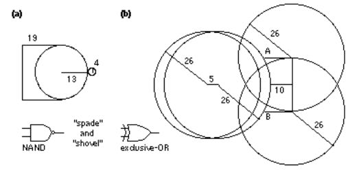
Figure 9.1 shows the spades and shovels, the recognized symbols for AND, NAND, OR, and NOR gates. One of the problems with these recommendations is that the corner points of the shapes do not always lie on a grid point (using a reasonable grid size).
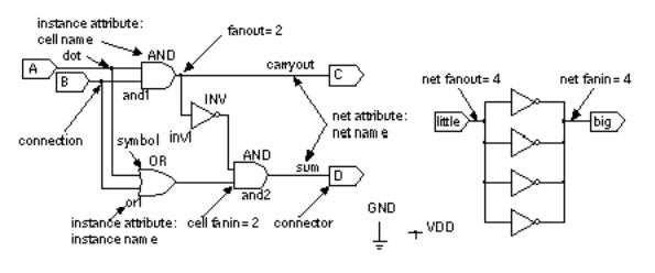
FIGURE 9.1 IEEE-recommended dimensions and their construction for logic-gate symbols. (a) NAND gate (b) exclusive-OR gate (an OR gate is a subset).
Figure 9.2 shows some pictorial definitions of objects you can use in a simple schematic. We shall discuss the different types of objects that might appear in an ASIC schematic first and then discuss the different types of connections.
FIGURE 9.2 Terms used in circuit schematics.
Schematic-entry tools for ASIC design are similar to those for printed-circuit board (PCB) design. The basic object on a PCB schematic is a component or device a TTL IC or resistor, for example. There may be several hundred components on a typical PCB. If we think of a logic gate on an ASIC as being equivalent to a component on a PCB, then a large ASIC contains hundreds of thousands of components. We can normally draw every component on a few schematic sheets for a PCB, but drawing every component on an ASIC schematic is impractical.
9.1.1 Hierarchical Design
Hierarchy reduces the size and complexity of a schematic. Suppose a building has 10 floors and contains several hundred offices but only three different basic office plans. Furthermore, suppose each of the floors above the ground floor that contains the lobby is identical. Then the plans for the whole building need only show detailed plans for the ground floor and one of the upper floors. The plans for the upper floor need only show the locations of each office and the office type. We can then use a separate set of three detailed plans for each of the different office types. All these different plans together form a nested structure that is a hierarchical design . The plan for the whole building is the top-level plan. The plans for the individual offices are the lowest level. To clarify the relationship between different levels of hierarchy we say that a subschematic (an office) is a child of the parent schematic (the floor containing offices). An electrical schematic can contain subschematics. The subschematic, in turn, may
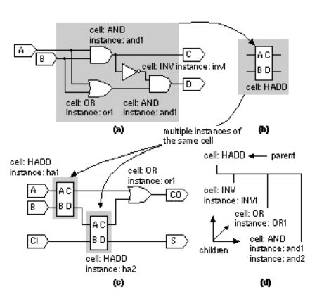
contain other subschematics. Figure 9.3 illustrates the principles of schematic hierarchical design.
FIGURE 9.3 Schematic example showing hierarchical design. (a) The schematic of a half-adder, the subschematic of cell HADD. (b) A schematic symbol for the half adder. (c) A schematic that uses the half-adder cell. (d) The hierarchy of cell HADD.
The alternative to hierarchical design is to draw all of the ASIC components on one giant schematic, with no hierarchy, in a flat design . For a modern ASIC containing thousands or more logic gates using a flat design or a flat schematic would be hopelessly impractical. Sometimes we do use flat netlists though.
9.1.2 The Cell Library
Components in an ASIC schematic are chosen from a library of cells. Library elements for all types of ASICs are sometimes also known as modules . Unfortunately the term module will have a very specific meaning when we come to discuss hardware description languages. To avoid any chance of confusion I use the term cell to mean either a cell, a module, a macro, or a book from an ASIC library. Library cells are equivalent to the offices in our office building.
Most ASIC companies provide a schematic library of primitive gates to be used for schematic entry. The first problem with ASIC schematic libraries is that there are no naming conventions. For example, a primitive two-input NAND gate in a Xilinx FPGA library does not have the same name as the two-input NAND gate
in an LSI Logic gate-array library. This means that you cannot take a schematic that you used to create a prototype product using a Xilinx FPGA and use that schematic to create an LSI Logic gate array for production (something you might very likely want to do). As soon as you start entering a schematic using a library from an ASIC vendor, you are, to some extent, making a commitment to use that vendor s ASIC. Most ASIC designers are much happier maintaining a large degree of vendor independence.
A second problem with ASIC schematic libraries is that there are no standards for cell behavior. For example, a two-input MUX in an Actel library operates so that the input labeled A is selected when the MUX select input S = '0'. A two-input MUX in a VLSI Technology library operates in the reverse fashion, so that the input labeled B is selected when S = '0'. These types of differences can cause hard-to-find problems when trying to convert a schematic from one vendor to another by hand. These problems make changing or retargeting schematics from one vendor to another difficult. This process is sometimes known as porting a design.
Library cells that represent basic logic gates, such as a NAND gate, are known as primitive cells , usually referred to just as cells. In a hierarchical ASIC design a cell may be a NAND gate, a flip-flop, a multiplier, or even a microprocessor, for example. To use the office building analogy again, each of the three basic office types is a primitive cell. However, the plan for the second floor is also a cell. The second-floor cell is a subschematic of the schematic for the whole building. Now we see why the commonly accepted use of the term cell in schematic entry can be so confusing. The term cell is used to represent both primitive cells and subschematics. These are two different, but closely related, things.
There are two types of macros for MGAs and programmable ASICs. The most common type of macro is a hard macro that includes placement information. A hard macro can change in position and orientation, but the relative location of the transistors, other layout, and wiring inside the macro is fixed. A soft macro contains only connection information (between transistors for a gate array or between logic cells for a programmable ASIC). Thus the placement and wiring for a soft macro can vary. This means that the timing parameters for a soft macro can only be determined after you complete the place-and-route step. For this reason the basic library elements for MGAs and programmable ASICs, such as NAND gates, flip-flops, and so on, are hard macros.
A standard cell contains layout information on all mask levels. An MGA hard macro contains layout information on just the metal, contact, and via layers. An MGA soft macro or programmable ASIC macro does not contain any layout information at all, just the details of connections to be made inside the macro.
We can stretch the office building analogy to explain the difference between hard and soft macros. A hard macro would be an office with fixed walls in which you are not allowed to move the furniture. A soft macro would be an office with partitions in which you can move the furniture around and you can also change
the shape of your office by moving the partitions.
9.1.3 Names
Each of the cells, primitive or not, that you place on an ASIC schematic has a cell name . Each use of a cell is a different instance of that cell, and we give each instance a unique instance name . A cell instance is somewhere between a copy and a reference to a cell in a library. An analogy would be the pictures of hamburgers on the wall in a fast-food restaurant. The pictures are somewhere between a copy and a reference to a real hamburger.
We represent each cell instance by a picture or icon , also known as a symbol . We can represent primitive cells, such as NAND and NOR gates, with familiar icons that look like spades and shovels. Some schematic editors offer the option of switching between these familiar icons and using the rectangular IEEE standard symbols for logic gates. Unfortunately the term icon is also often used to refer to any of the pictures on a schematic, including those that represent subschematics. There is no accepted way to differentiate between an icon that represents a primitive cell and one that represents a subschematic that may be in turn a collection of primitive cells. In fact, there is usually no easy way to tell by looking at a schematic which icons represent primitive cells and which represent subschematics.
We will have three different icons for each of the three different primitive offices in the imaginary office building example of Section 9.1.1 . We also will have icons to represent the ground floor and the plan for the other floors. We shall call the common plan for the second through tenth floors, Floor . Then we say that the second floor is an instance of the cell name Floor . The third through tenth floors are also instances of the cell name Floor . The same icon will be used to represent the second through tenth floors, but each will have a unique instance name. We shall give them instance names: FloorTwo , FloorThree , ... , FloorTen . We say that FloorTwo through FloorTen are unique instance names of the cell name Floor .
At the risk of further confusion I should point out that, strictly speaking, the definition of a primitive cell depends on the type of library being used. Schematic-entry libraries for the ASIC designer stop at the level of NAND gates and other similar low-level logic gates. Then, as far as the ASIC designer is concerned, the primitive cells are these logic gates. However, from the view of the library designer there is another level of hierarchy below the level of logic gates. The library designer needs to work with libraries that contain schematics of the gates themselves, and so at this level the primitive cells are transistors.
Let us look at the building analogy again to understand the subtleties of primitive cells. A building contractor need only concern himself with the plans for our office building down to the level of the offices. To the building contractor the primitive cells are the offices. Suppose that the first of the three different office
types is a corner office, the second office type has a window, and a third office type is without a window. We shall call these office cells: CornerOffice , WindowOffice , and NoWindowOffice . These cells are primitive cells as far as the contractor is concerned. However, when discussing the plans with a client, the architect of our building will also need to see how each offices is furnished. The architect needs to see a level of detail of each office that is more complicated than needed by the building contractor. The architect needs to see the cells that represent the tables, chairs, and desks that make up each type of office. To the architect the primitive cells are a library containing cells such as chair , table , and desk .
9.1.4 Schematic Icons and Symbols
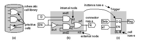
Most schematic-entry programs allow the designer to draw special or custom icons. In addition, the schematic-entry tool will also usually create an icon automatically for a subschematic that is used in a higher-level schematic. This is a derived icon , or derived symbol . The external connections of the subschematic are automatically attached to the icon, usually a rectangle.
Figure 9.4 (c) shows what a derived icon for a cell, DLAT , might look like (we could also have drawn this by hand). The subschematic for DLAT is shown in Figure 9.4 (b). We say that the inverter with the instance name inv1 in the subschematic is a subcell (or submodule) of the cell DLAT . Alternatively we say that cell instance inv1 is a child of the cell DLAT , and cell DLAT is a parent of cell instance inv1 .
FIGURE 9.4 A cell and its subschematic. (a) A schematic library containing icons for the primitive cells. (b) A subschematic for a cell, DLAT, showing the instance names for the primitive cells. (c) A symbol for cell DLAT.
Figure 9.5 (a) shows a more complex subschematic for a 4-bit latch. Each primitive cell instance in this schematic must have a unique name. This can get very tiresome for large circuits. Instead of creating complex, but repetitive, subschematics for complex cells we can use hierarchy.
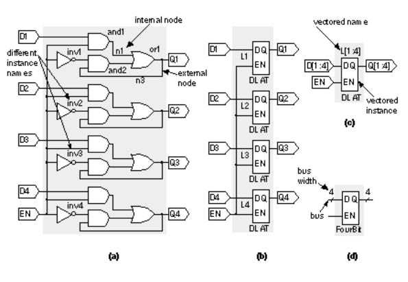
FIGURE 9.5 A 4-bit latch: (a) drawn as a flat schematic from gate-level primitives, (b) drawn as four instances of the cell symbol DLAT, (c) drawn using a vectored instance of the DLAT cell symbol with cardinality of 4,
(d) drawn using a new cell symbol with cell name FourBit.
Figure 9.5 (b) shows a hierarchical subschematic for a cell FourBit , which in turn uses four instances of the cell DLAT . The four instances of DLAT in Figure 9.5 (b) have different instance names: L1 , L2 , L3 , and L4 . Notice that we cannot use just one name for the four instances of DLAT to indicate that they
are all the same cell. If we did, we could not differentiate between L1 and L2 , for example.
The vertical row of instances in Figure 9.5 (b) looks like a vector of elements. Figure 9.5 (c) shows a vectored instance representing four copies of the DLAT cell. We say the cardinality of this instance is 4. Tools normally use bold lines or some other distinguishing feature to represent a vectored instance. The cardinality information is often shown as a vector. Thus L[1:4] represents four instances: L[1] , L[2] , L[3] , L[4] . This is convenient because now we can see that all subcells are identical copies of L , but we have a unique name for each.
Finally, as shown in Figure 9.5 (d) we can create a new symbol for the 4-bit latch, FourBit . The symbol for FourBit has a 4-bit-wide input bus for the four D inputs, and a 4-bit wide output bus for the four Q outputs. The subschematic for FourBit could be either Figure 9.5 (a), (b), or (c) (though the exact naming of the inputs and outputs and their attachment to the buses may be different in each case).
We need a convention to distinguish, for example, between the inverter subcells, inv1 , which are children of the cell DLAT , which are in turn children of the cell FourBit . Most schematic-entry tools do this by combining the instance names of the subcells in a hierarchical manner using a special character as a delimiter. For example, if we drew the subschematic as in Figure 9.5 (b), the four inverters in FourBit might be named L1.inv1 , L2.inv1 , L3.inv1 , and L4.inv1 . Once again this makes it clear that the inverters, inv1 , are identical in all four subcells.
In our office building example, the offices are subcells of the cell Floor . Suppose you and I both have corner offices. Mine is on the second floor and yours is above mine on the third floor. My office is 211 and your office is 311. Another way to name our offices on a building plan might be FloorTwo.11 for my office and FloorThree.11 for your office. This shows that FloorTwo.11 is a subcell of FloorTwo and also makes it clear that, apart from being on different floors, your office and mine are identical. Both our offices have instance names 11 and are instances of cell name Corner .
9.1.5 Nets
The schematics shown in Figure 9.4 contain both local nets and external nets . An example of a local net in Figure 9.4 (b) is n1 , the connection between the output terminal of the AND cell and1 to the OR cell or1 . When the four copies of this circuit are placed in the parent cell FourBit in Figure 9.5 (d), four copies of net n1 are created. Since the four nets named n1 are not actually electrically connected, even though they have the same name at the lowest hierarchical level, we must somehow find a way to uniquely identify each net.
The usual convention for naming nets in a hierarchical schematic uses the parent cell instance name as a prefix to the local net name. A special character ( ':' '/' '$' '#' for example) that is not allowed to appear in names is used as a delimiter to separate the net name from the cell instance name. Supposing that we drew the subschematic for cell FourBit as shown in Figure 9.5 (b), the four different nets labeled n1 might then become:
FourBit .L1:n1 FourBit .L2:n1 FourBit .L3:n1 FourBit .L4:n1
This naming is usually done automatically by the schematic-entry tool.
The schematic DLAT also contains three external nets: D, EN, and Q . The terminals on the symbol DLAT connect these nets to other nets in the hierarchical level above. For example, the signal Trigger:flag in Figure 9.4 (c) is also Trigger.DLAT:Q . Each schematic tool handles this situation differently, and life becomes especially difficult when we need to refer to these nodes from a simulator outside the schematic tool, for example. HDLs such as VHDL and Verilog have a very precise and well-defined standard for naming nets in hierarchical structures.
9.1.6 Schematic Entry for ASICs and PCBs
A symbol on a schematic may represent a component, which may contain component parts. You are more likely to come across the use of components in a PCB schematic. A component is slightly different from an ASIC library cell. A simple example of a component would be a TTL gate, an SN74LS00N, that contains four 2-input NAND gates. We call an SN74LS00N a component and each of the individual NAND gates inside is a component part. Another common example of a component would be a resistor pack a single package that contains several identical resistors.
In PCB design language a component label or name is a reference designator . A reference designator is a unique name attribute, such as R99 , attached to each component. A reference designator, such as R99 , has two pieces: an alpha prefix R and a numerical suffix 99 . To understand the difference between reference designators and instance names, we need to look at the special requirements of PCB design.
PCBs usually contain packaged ASICs and other ICs that have pins that are soldered to a board. For rectangular, dual-in-line (DIP) packages the pins are numbered counterclockwise from the upper-left corner looking down on the package.
IC symbols have a pin number for each part in the package. For example, the TTL 74174 hex D flip-flop with clear, contains six parts: six identical D flip-flops. The IC symbol representing this device has six PinNumber attribute entries for the D input corresponding to the six possible input pins. They are pins 3, 4, 6, 11, 13, and 14.
When we need a flip-flop in our design, we use a symbol for a 74174 from a schematic library, suppose the symbol name is dffClr . We shall assign a unique instance name to the symbol, CarryFF . Now suppose we need another, identical, flip-flop and we call this BitFF . We do not mind which of the six flip-flop parts in a 74174 we use for CarryFF and BitFF . In fact they do not even have to be in the same package. We shall delay the choice of assigning CarryFF and BitFF to specific packages until we get to the PCB routing step. So at this point on our schematic we do not even know the pin numbers for CarryFF and BitFF . For example the D input to CarryFF could be pin 3, 4, 6, 11, 13, or 14.
The number of wire crossings on a PCB is minimized by careful assignment of components to packages and choice of parts within a package. So the placement-and-routing software may decide which part of which package to use for CarryFF and BitFF depending on which is easier to route. Then, only after the placement and routing is complete, are unique reference designators assigned to the component parts. Only at this point do we know where CarryFF is actually located on the PCB by referring to the reference designator, which points to a specific part in a specific package. Thus CarryFF might be located in IC4 on our PCB. At this point we also know which pins are used for each symbol. So we
now know, for example, that the D-input to CarryFF is pin 3 of IC4 .
There is no process in ASIC design directly equivalent to the process of part assignment described above and thus no need to use reference designators. The reference-designator naming convention quickly becomes unwieldy if there are a large number of components in a design. For example, how will we find a NAND gate named X3146 in an ASIC schematic with 100 pages? Instead, for ASICs, we use a naming scheme based on hierarchy.
In large hierarchical ASIC designs it is difficult to provide a unique reference designator to each element. For this reason ASIC designs use instance names to identify the individual components. Meaningful names can be assigned to low-level components and also the symbols that represent hierarchy. We derive the component names by joining all of the higher level cell names together. A special character is used as a delimiter and separates each level.
Examples of hierarchical instance names are:
cpu.alu.adder.and01
MotherBoard:Cache:RAM4:ReadBit4:Inverter2
9.1.7 Connections
Cell instances have terminals that are the inputs and outputs of the cell. Terminals are also known as pins , connectors , or signals . The term pin is widely used, but we shall try to use terminal, and reserve the term pin for the metal leads on an ASIC package. The term pin is used in schematic entry and routing programs that are primarily intended for PCB design.
FIGURE 9.6 An example of the use of a bus to simplify a schematic. (a) An address decoder without using a bus. (b) A bus with bus rippers simplifies the schematic and reduces the possibility of making a mistake in creating and reading the schematic.
Electrical connections between cell instances use wire segments or nets . We can group closely related nets, such as the 32 bits of a 32-bit digital word, together
into a bus or into buses (not busses). If signals on a bus are not closely related, we usually use the term bundle or array instead of bus. An example of a bundle might be a bus for a SCSI disk system, containing not only data bits but handshake and control signals too. Figure 9.6 shows an example of a bus in a schematic. If we need to access individual nets in a bus or a bundle, we use a breakout (also known as a ripper , an EDIF term, or extractor ). For example, a breakout is used to access bits 0 7 of a 32-bit bus. If we need to rearrange bits on a bus, some schematic editors offer something called a swizzle . For example, we might use a swizzle to reorder the bits on an 8-bit bus so that the MSB becomes the LSB and so on down to the LSB, which now becomes the MSB. Swizzles can be useful. For example, we can multiply or divide a number by 2 by swizzling all the bits up or down one place on a bus.
9.1.8 Vectored Instances and Buses
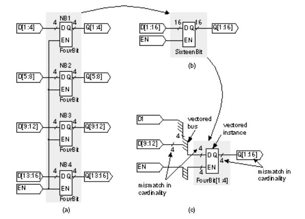
So far the naming conventions are fairly standard and easy to follow. However, when we start to use vectored instances and buses (as is now common in large ASICs), there are potential areas of difficulty and confusion. Figure 9.7 (a) shows a schematic for a 16-bit latch that uses multiple copies of the cell FourBit . The buses are labeled with the appropriate bits. Figure 9.7 (b) shows a new cell symbol for the 16-bit latch with 16-bit wide buses for the inputs, D, and outputs, Q.
FIGURE 9.7 A 16-bit latch: (a) drawn as four instances of cell FourBit; (b) drawn as a cell named SixteenBit; (c) drawn as four multiple instances of cell FourBit.
Figure 9.7 (c) shows an alternative representation of the 16-bit latch using a vectored instance of FourBit with cardinality 4. Suppose we wish to make a connection to expressly one bit, D1 (we have used D1 as the first bit rather than the more conventional D0 so that numbering is easier to follow). We also wish to make a connection to bits D9 D12, represented as D[9:12]. We do this using a bus ripper. Now we have the rather awkward situation of bus naming shown in Figure 9.7 (c). Problems arise when we have buses of buses because the numbers for the bus widths do not match on either side of a ripper. For this reason it is best to use the single-bus approach shown in Figure 9.7 (b) rather than the vectored-bus approach of Figure 9.7 (c).
9.1.9 Edit-in-Place
Figure 9.7 (b) shows a symbol SixteenBit , which uses the subschematic shown in Figure 9.7 (a) containing four copies of FourBit , named NB1 , NB2 , NB3 , and NB4 (the NB stands for nibble, which is half of a word; a nibble is 4 bits for 8-bit words). Suppose we use the schematic-entry program to edit the subcell NB1.L1 , which is an instance of DLAT inside NB1 . Perhaps we wish to change the D latch to a D latch with a reset, for example. If the schematic editor supports edit-in-place , we can edit a cell instance directly. After we edit the cell, the program will update all the DLAT subcells in the cell that is currently loaded to reflect the changes that have been made.
To see how edit-in-place works, consider our office building again. Suppose we wish to change some of the offices on each floor from offices without windows to offices with windows. We select the cell instance FloorTwo that is, an instance of cell Floor . Now we choose the edit mode in the schematic-entry program. But wait! Do we want to edit the cell Floor , or do we want to edit the cell instance FloorTwo ? If we edit the cell Floor , we will be making changes to all of the floors that use cell name Floor that is, instances FloorTwo through FloorTen . If we edit the cell instance FloorTwo , then the second floor will become different from all the other floors. It will no longer be an instance of cell name Floor and we will have to create another cell name for the cell used by instance FloorTwo . This is like the difference between ordering just one hamburger without pickles and changing the picture on the wall that will change all future hamburgers.
Using edit-in-place we can edit the cell Floor . Suppose we change some of the cell instances of cell name NoWindowOffice to instances of cell name WindowOffice . When we finish editing and save the cell Floor , we have effectively changed all of the floors that contain instances of this cell.
Instead of editing a cell in place, you may really want to edit just one instance of a cell and leave any other instances unchanged. In this case you must create a new cell with a new symbol and new, unique cell name. It might also be wise to change the instance name of the new cell to avoid any confusion.
For example, we might change the third-floor plan of our office to be different from the other upper floors. Suppose the third floor is now an instance of cell name FloorVIP instead of Floor . We could continue to call the third floor cell instance FloorThree , but it would be better to rename the instance differently, FloorSpecial for example, to make it clear that it is different from all the other floors.
Some tools have the ability to alias nets. Aliasing creates a net name from the highest level in the design. Local names are net names at the lowest level such as D , and Q in a flip-flop cell. These local names are automatically replaced by the appropriate top-level names such as Clock1 , or Data2 , using a dictionary . This greatly speeds tracing of signals through a design containing many levels of hierarchy.
9.1.10 Attributes
You can attach a name , also known as an identifier or label , to a component, cell instance, net, terminal, or connector. You can also attach an attribute , or property , which describes some aspect of the component, cell instance, net, or connector.
Each attribute has a name, and some attributes also have values. The most common problems in working with schematics and netlists, especially when you try to exchange schematic information between different tools, are problems in naming.
Since cells and their contents have to be stored in a database, a cell name frequently corresponds (or is mapped to) a filename. This then raises the problems of naming conventions including: case sensitivity, name-collision resolution, dictionaries, handling of common special characters (such as embedded blanks or underscores), other special characters (such as characters in foreign alphabets), first-character restrictions, name-length problems (only 28 characters are permitted on an NFS compatible filename), and so on.
9.1.11 Netlist Screener
A surprising number of problems can be found by checking a schematic for obviously fatal errors. A program that analyzes a schematic netlist for simple errors is sometimes called a schematic screener or netlist screener . Errors that can be found by a netlist screener include:
●unconnected cell inputs,
●unconnected cell outputs,
●nets not driven by any cells,
●too many nets driven by one cell,
●nets driven by more than one cell.
The screener can work continuously as the designer is creating the schematic or can be run as a separate program independently from schematic entry. Usually
the designer provides attributes that give the screener the information necessary to perform the checks. A few of the typical attributes that schematic-entry programs use are described next.
A screener usually generates a list of errors together with the locations of the problem on the schematic where appropriate. Some editors associate an identifier, or handle , to every piece of a schematic, including comments and every net. Normally there is some convention to the assigned names such as a grid on a schematic. This works like the locator codes on a map, so that a net with A1 as part of the name is in the upper-left-hand corner, for example. This allows you to quickly and uniquely find any problems found by a screener. The term handle is a computer programming term that is used in referring to a location in memory. Each piece of information on a schematic is stored in lists in memory. This technique breaks down completely when we move to HDLs.
Most schematic-entry programs work on a grid. The designer can control the size of the grid and whether it is visible or not. When you place components or wires you can instruct the editor to force your drawing to snap to grid . This means that drawing a schematic is like drawing on graph paper. You can only locate symbols, wires, and connections on grid points. This simplifies the internal mechanics of the schematic-entry program. It also makes the transfer of schematics between different EDA systems more manageable. Finally, it allows the designer to produce schematic diagrams that are cleaner in appearance and thus easier to read.
Most schematic-entry programs allow you to find components by instance name or cell name. The editor may either jump to the component location and center the graphic window on the component or highlight the component. More sophisticated options allow more complex searches, perhaps using wildcard matching. For example, to find all three-input NAND gates (primitive cell name ND3) or three-input NOR gates (primitive cell name NO3), you could search for cell name N*3, where * is a wildcard symbol standing for any character. The editor may generate a list of components, perhaps with page number and coordinate locations. Extensive find features are useful for large schematics where it quickly becomes impossible to find individual components.
Some schematic editors can complete automatic naming of reference designators or instance names to the schematic symbols either as the editor is running or as a postprocessing step. A component attribute, called a prefix, defines the prefix for the name for each type of component. For example, the prefix for all resistor component types may be R . Each time a prefix is found or a new instance is placed, the number in the reference designator or name is automatically incremented. Thus if the last resistor component type you placed was R99 , the next time you place a resistor it would automatically be named R100 .
For large schematics it is useful to be able to generate a report on the used and unused reference designators. An example would be:
Reference designator prefix: R
Unused reference designator numbers: 153, 154
Last used reference designator number: 180
If you need this feature, you probably are not using enough hierarchy to simplify your design.
During schematic entry of an ASIC design you will frequently need multiple copies of components. This often occurs during datapath design, where operations are carried out across multiple signals on a bus. A common example would be multiple copies of a latch, one for each signal on a bus. It is tedious and inefficient to have to draw and label the same cell many times on a schematic. To simplify this task, most editors allow you to place a special vectored cell instance of a cell. A vectored cell instance, or vectored instance for short, uses the same icon for a single instance but with a special attribute, the cell cardinality , that denotes the number of copies of the cell. Connections between signals on a bus and vectored instances should be handled automatically. The width or cardinality of the bus and the cell cardinality must match, and the design-entry tool should issue a warning if this is not the case.
A schematic-entry program can use a terminal attribute to determine which cell terminals are output terminals and which terminals are input terminals. This attribute is usually called terminal polarity or terminal direction . Possible values for terminal polarity might be: input , output , and bidirectional . Checking the terminal polarity of the terminals on a net can help find problems such as a net with all input terminals or all output terminals.
The fanout of a cell measures the driving capability of an output terminal. The fanin of a cell measures the number of input terminals. Fanout is normally measured using a standard load. A standard load is the load presented by one input of a primitive cell, usually a two-input NAND. For example, a library cell Counter may have an input terminal, Clock , that is connected to the input terminals of five primitive cells. The loading at this terminal is then five standard loads. We say that the fanout of Clock is five. In a similar fashion, we say that if a cell Buffer is capable of driving the inputs of three primitive cells, the fanout of Buffer is three. Using the fanin and fanout attributes a netlist screener can check to see if the fanout driving a net is greater than the sum of all loads on that net. (See Figure 9.2 on page 329.)
9.1.12 Schematic-Entry tools
Some editors offer icon edit-in-place in a similar fashion as schematic edit-in-place for cells. Often you have to toggle editing modes in the schematic-entry program to switch between editing cells and editing cell icons. A schematic-entry program must keep track of when cells are edited. Normally this is done by using a timestamp or datestamp for each cell. This is a text field within
the data file for each cell that holds the date and time that the cell was last modified. When a new schematic or cell is loaded, the program needs to compare its timestamp with the timestamps of any subcells. If any of the subcell timestamps are more recent, then the designer needs to be alerted. Usually a message appears to inform you that changes have been made to subcells since the last time the cell currently loaded was saved. This may be what you expect or it may be a warning that somehow a subcell has been changed inadvertently (perhaps someone else changed it) since you last loaded that cell.
Normally the primitive cells in a library are locked and cannot be edited. If you can edit a primitive cell, you have to make a copy, edit the copy, and rename it. Normally the ASIC designer cannot do this and does not want to. For example, to edit a primitive NAND gate stored in an ASIC schematic library would require that the subschematic of the primitive cell be available (usually not the case) and also that the next lower level primitives (symbols for the transistors making up the NAND gate) also be available to the designer (also usually not the case).
What do you do if somehow changes were made to a cell by mistake, perhaps by someone else, and you don t want the new cell, you want the old version? Most schematic-entry and other EDA tools keep old versions of files as a back-up in case this kind of problem occurs. Most EDA software automatically keeps track of the different versions of a file by appending a version number to each file. Usually this is transparent to the designer. Thus when you edit a cell named Floor , the file on disk might be called Floor.6 . When you save the changes, the software will not overwrite Floor.6 , but write out a new file and automatically name it Floor.7 .
Some design-entry tools are more sophisticated and allow users to create their own libraries as they complete an ASIC design. Designers can then control access to libraries and the cells that they build during a design. This normally requires that a schematic editor, for example, be part of a larger EDA system or framework rather than work as a stand-alone tool. Sometimes the process of library control operates as a separate tool, as a design manager or library manager
. Often there is a program similar to the UNIX make command that keeps track of all files, their dependencies, and the tools that are necessary to create and update each file.
You can normally set the number of back-up versions of files that EDA software keeps. The version history controls the number of files the software will keep. If you accidentally update, overwrite, or delete a file, there is usually an option to select and revert to an earlier version. More advanced systems have check-out services (which work just as in source control systems in computer programming databases) that prevent these kinds of problems when many people are working on the same design. Whenever possible, the management of design files and different versions should be left under software control because the process can become very complicated. Reverting to an earlier version of a cell can have drastic consequences for other cells that reference the cell you are working with. Attempts to manually edit files by changing version numbers and timestamps can
quickly lead to chaos.
Most schematic-entry programs allow you to undo commands. This feature may be restricted to simply undoing the last command that you entered, or may be an unlimited undo and redo, allowing you to back up as many commands as you want in the current editing session.
You can spend a lot of time in a schematic editor placing components and drawing the connections between them. Features that simplify initial entry and allow modifications to be made easily can make an enormous difference to the efficiency of the schematic-entry process.
Most schematic editors allow you to make connections by dragging the cursor with the wire following behind, in a process known as rubber banding . The connection snaps to a right angle when the connection is completed. For wire connections that require more than two line segments, an automatic wiring feature is useful. This allows you to define the wire path roughly using mouse clicks and have the editor complete the connection.
It is exceedingly painful to move components if you have to rewire connections each time. Most schematic editors allow you to move the components and drag any wires along with them.
One of the most annoying problems that can arise in schematic entry is to think that you have joined two wires on a schematic but find that in reality they do not quite meet. This error can be almost impossible to find. A good editing program will have a way of avoiding this problem. Some editors provide a visual (flash) or audible (beep) feedback when the designer draws a wire that makes an electrical connection with another. Some editors will also automatically insert a dot at a T connection to show that an electrical connection is present. Other editors refuse to allow four-way connections to be made, so there can be no ambiguity when wires cross each other if an electrical connection is present or not.
A cell library or a collection of libraries is a key part of the schematic-entry process. The ability to handle and control these libraries is an important feature of any schematic editor. It should be easy to select components from the library to be placed on a schematic.
In large schematics it is necessary to continue large nets and signals across several pages of schematics. Signals such as power and ground, VDD and GND, can be connected using global nets or special connectors . Global nets allow the designer to label a net with the same name at different places on a schematic page or on different pages without having to draw a connection explicitly. The schematic editor treats these nets as though they were electrically connected. Special connector symbols can be used for connections that cross schematic pages. An off-page connector or multipage connector is a special symbol that will show and label a connection to different schematic pages. More sophisticated editors can automatically label these connectors with the page numbers of the destination connectors.

9.1.13 Back-Annotation
After you enter a schematic you simulate the design to make sure it works as expected. This completes the logical design. Next you move to ASIC physical design and complete the layout. Only after you complete the layout do you know the parasitic capacitance and therefore the delay associated with the interconnect. This postroute delay information must be returned to the schematic in a process known as back-annotation . Then you can complete a final, postlayout simulation to make sure that the specifications for the ASIC are met. Chapter 13 covers simulation, and the physical design steps are covered in Chapters 15 to 17.
9.2 Low-Level Design
Languages
Schematics can be a very effective way to convey design information because pictures are such a powerful medium. There are two major problems with schematic entry, however. The first problem is that making changes to a schematic can be difficult. When you need to include an extra few gates in the middle of a schematic sheet, you may have to redraw the whole sheet. The second problem is that for many years there were no standards on how symbols should be drawn or how the schematic information should be stored in a netlist. These problems led to the development of design-entry tools based on text rather than graphics. As TTL gave way to PLDs, these text-based design tools became increasingly popular as de facto standards began to emerge for the format of the design files.
PLDs are closely related to FPGAs. The major advantage of PLD tools is their low cost, their ease of use, and the tremendous amount of knowledge and number of designs, application notes, textbooks, and examples that have been built up over years of their use. It is natural then that designers would want to use PLD development systems and languages to design FPGAs and other ASICs. For example, there is a tremendous amount of PLD design expertise and working designs that can be reused.
In the case of ASIC design it is important to use the right tool for the job. This may mean that you need to convert from a low-level design medium you have used for PLD design to one more appropriate for ASIC design. Often this is because you are merging several PLDs into a single, much larger, ASIC. The reason for covering the PLD design languages here is not to try and teach you how to use them, but to allow you to read and understand a PLD language and, if necessary, convert it to a form that you can use in another ASIC design system.
9.2.1 ABEL
ABEL is a PLD programming language from Data I/O. Table 9.2 shows some examples of the ABEL statements. The following example code describes a 4:1 MUX (equivalent to the LS153 TTL part):
TABLE 9.2 ABEL. |
|
|
Statement |
Example |
Comment |
Module |
module MyModule |
You can have multiple modules. |
Title
Device
Comment
title 'Title in a String'
MYDEV device '22V10'
;
"comments go between double quotes"
"end of line is end of comment
A string is a character series between quotes.
MYDEV is Device ID for documentation.
22V10 is checked by the compiler.
The end of a line signifies the end of a comment; there is no need for an end quote.
@ALTERNATE |
@ALTERNATE "use |
operator |
alternate |
default |
|
|
alternate symbols |
|
|
|
|
|
|
AND |
* |
& |
|
|
|
OR |
+ |
# |
|
|
|
NOT |
/ |
! |
|
|
|
XOR |
:+: |
$ |
|
|
|
XNOR |
:*: |
!$ |
|
|
MYINPUT pin 2; I3, I4 |
Pin 22 is the IO for input on pin 2 for |
|||
|
a 22V10. |
|
|
||
Pin declaration |
pin 3, 4 ; |
MYOUTPUT is active-low at the |
|||
/MYOUTPUT pin 22; |
|||||
|
chip pin. |
|
|
||
|
IO3,IO4 pin 21,20 ; |
Signal names must start with a letter. |
|||
|
|
||||
Equations |
equations |
Defines combinational logic. |
|||
|
IO4 = HELPER ; |
Two-pass logic |
|
||
|
HELPER = /I4 ; |
|
|||
|
|
|
|
||
Assignments |
MYOUTPUT = |
Equals '=' is unlocked assignment. |
|||
/MYINPUT ; |
|||||
|
|
|
|
||
|
IO3 := I4 ; |
Clocked assignment operator |
|||
|
(registered IO) |
|
|||
|
|
|
|||
Signal sets |
D = [D0, D1, D2, D3] ; |
A signal set, an ABEL bus |
|
||
Q = [Q0, Q1, Q2, Q3]; |
|
||||
|
|
|
|
||
|
Q := D ; |
4-bit-wide register |
|
||
Suffix |
MYOUTPUT.RE = CLR |
Register reset |
|
||
|
; |
|
|
|
|
|
MYOUTPUT.PR = PRE |
Register preset |
|
||
|
; |
|
|
|
|
COUNT = [D0, D1, D2]; Can t use @ALTERNATE
Addition
COUNT := COUNT + 1; if you use '+' to add.
|
ENABLE IO3 = IO2; |
Three-state enable (ENABLE is a |
|
Enable |
keyword). |
||
|
|||
IO3 = MYINPUT; |
|
||
|
IO3 must be a three-state pin. |
||
|
|
||
Constants |
K = [1, 0, 1] ; |
K is 5. |
|
Relational |
IO# = D == K5 ; |
Operators: == != < > <= >= |
|
End |
end MyModule |
Last statement in module |
|
module MUX4 |
|
|
|
title '4:1 MUX' |
|
|
MyDevice device 'P16L8' ;
@ALTERNATE
"inputs
A, B, /P1G1, /P1G2 pin 17,18,1,6 "LS153 pins 14,2,1,15
P1C0, P1C1, P1C2, P1C3 pin 2,3,4,5 "LS153 pins 6,5,4,3
P2C0, P2C1, P2C2, P2C3 pin 7,8,9,11 "LS153 pins 10,11,12,13
"outputs
P1Y, P2Y pin 19, 12 "LS153 pins 7,9
equations
P1Y = P1G*(/B*/A*P1C0 + /B*A*P1C1 + B*/A*P1C2 + B*A*P1C3);
P1Y = P1G*(/B*/A*P1C0 + /B*A*P1C1 + B*/A*P1C2 + B*A*P1C3);
end MUX4
9.2.2 CUPL
CUPL is a PLD design language from Logical Devices. We shall review the CUPL 4.0 language here. The following code is a simple CUPL example describing sequential logic:
SEQUENCE BayBridgeTollPlaza {
PRESENT red
IF car NEXT green OUT go; /* conditional synchronous output */
DEFAULT NEXT red; /* default next state */
PRESENT green
NEXT red; } /* unconditional next state */
This code describes a state machine with two states. Table 9.3 shows the different state machine assignment statements.
TABLE 9.3 CUPL statements for state-machine entry.
Statement |
|
Description |
IF |
NEXT |
Conditional next state transition |
IF |
NEXT OUT Conditional next state transition with synchronous |
|
|
|
output |
|
NEXT |
Unconditional next state transition |
|
NEXT OUT Unconditional next state transition with asynchronous |
|
|
|
output |
|
|
OUT Unconditional asynchronous output |
IF |
|
OUT Conditional asynchronous output |
DEFAULT NEXT |
Default next state transition |
|
DEFAULT |
|
OUT Default asynchronous output |
DEFAULT NEXT OUT Default next state transition with synchronous output
You may also encode state machines as truth tables in CUPL. Here is another simple example:
FIELD input = [in1..0];
FIELD output = [out3..0];
TABLE input => output {00 => 01; 01 => 02; 10 => 04; 11 => 08; }
The advantage of the CUPL language, and text-based PLD languages in general, is now apparent. First, we do not have to enter the detailed logic for the state decoding ourselves the software does it for us. Second, to make changes only requires simple text editing fast and convenient.
Table 9.4 shows some examples of CUPL statements. In CUPL Boolean equations may use variables that contain a suffix, or an extension , as in the following example:
output.ext = (Boolean expression); |
|
||
TABLE 9.4 CUPL. |
|
||
Statement |
Example |
Comment |
|
Boolean |
A = !B; |
Logical negation |
|
expression |
|||
|
|
||
|
A = B & C; |
Logical AND |
|
|
A = B # C; |
Logical OR |
|
|
A = B $ C; |
Logical exclusive-OR |
|
Comment |
A = B & C /* comment */ |
|
|
Pin declaration |
PIN 1 = CLK; |
Device dependent |
|
|
PIN = CLK; |
Device independent |
|
Node declaration NODE A; |
Number automatically assigned |
||
|
NODE [B0..7]; |
Array of buried nodes |
|
Pinnode |
PINNODE 99 = A; |
Node assigned by designer |
|
declaration |
|||
|
|
||
|
PINNODE [10..17] = [B0..7]; Array of pinnodes |
||
Bit-field |
FIELD Address = [B0..7]; |
8-bit address field |
|
declaration |
|||
|
|
||
Bit-field |
add_one = Address:FF; |
True if Address = OxFF |
|
operations |
|||
|
|
||
|
add_zero = !(Address:&); |
True if Address = Ox00 |
|
|
add_range = |
|
|
Address:[0F..FF];
True if 0F.LE.Address.LE.FF
The extensions steer the software, known as a fitter , in assigning the logic. For example, a signal-name suffix of .OE marks that signal as an output enable.
Here is an example of a CUPL file for a 4-bit counter placed in an ATMEL PLD part that illustrates the use of some common extensions:
Name 4BIT; Device V2500B; /* inputs */
pin 1 = CLK; pin 3 = LD_; pin 17 = RST_; pin [18,19,20,21] = [I0,I1,I2,I3];
/* outputs */
pin [4,5,6,7] = [Q0,Q1,Q2,Q3]; field CNT = [Q3,Q2,Q1,Q0]; /* equations */
Q3.T = (!Q2 & !Q1 & !Q0) & LD_ & RST_ /* count down */
#Q3 & !RST_ /* ReSeT */
#(Q3 $ I3) & !LD_; /* LoaD*/
Q2.T = (!Q1 & !Q0) & LD_ & RST_ # Q2 & !RST_ # (Q2 $ I2) & !LD_; Q1.T = !Q0 & LD_ & RST_ # Q1 & !RST_ # (Q1 $ I1) & !LD_;
Q0.T = LD_ & RST_ # Q0 & !RST_ # (Q0 $ I0) & !LD_; CNT.CK = CLK; CNT.OE = 'h'F; CNT.AR = 'h'0; CNT.SP = 'h'0;
In this example the suffix extensions have the following effects: .CK marks the

clock; .T configures sequential logic as T flip-flops; .OE (wired high) is the output enable; .AR (wired low) is the asynchronous reset; and .SP (wired low) is the synchronous preset. Table 9.5 shows the different CUPL extensions.
TABLE 9.5
Extension 1
D
L
J, K
S, R
T
DQ
LQ
AP, AR
SP, SR
CK
OE
CA
PR
CE
LE
OBS
CUPL 4.0 extensions.
Explanation
L D input to a D register
L L input to a latch
L J-K-input to a J-K register
L S-R input to an S-R register
L T input to a T register
R D output of an input D register
R Q output of an input latch
L Asynchronouspreset/reset
L Synchronouspreset/reset
L Product(async.) clock term
LProduct-term output enable
L Complement array L Programmablepreload
L CE input of a
D-CE register
L Productenable -term latch
Programmable L observability of buried nodes
Extension
DFB
LFB
TFB
INT
IO
IOD/T
IOL
IOAP,
IOAR
IOSP, IOSR
IOCK
APMUX, ARMUX
CKMUX
LEMUX
OEMUX
IMUX
TEC
Explanation
D register feedback of
R
combinational output
Latched feedback of
R
combinational output
T register feedback of
R
combinational output
R Internal feedback
R Pin feedback of registered output
R D/T register on pin feedback path selection
Latch on pin feedback path
R
selection
Asynchronous preset/reset of
L
register on feedback path
Synchronous preset/reset of
L
register on feedback path
L Clock for pin feedback register
Asynchronous preset/reset
L
multiplexor selection
L Clock multiplexor selector
L Latch enable multiplexor selector
Output enable multiplexor
L
selector
Input multiplexor selector of
L
two pins
L Technologyselection -dependent fuse
BYP |
L |
Programmable |
T1 |
L T1 input of 2-T register |
|
|
register bypass |
|
|
The 4-bit counter is a very simple example of the use of the Atmel ATV2500B. This PLD is quite complex and has many extra buried features. In order to use these features in CUPL (and ABEL) you need to refer to special pin numbers and node numbers that are given in tables in the manufacturer s data sheets. You may need the pin-number tables to reverse engineer or convert a complicated CUPL (or ABEL) design from one format to another.
Atmel also gives skeleton headers and pin declarations for their parts in their data sheets. Table 9.6 shows the headers and pin declarations in ABEL and CUPL format for the ATMEL ATV2500B.
TABLE 9.6 ABEL and CUPL pin declarations for an ATMEL ATV2500B.
ABEL
device_id device 'P2500B'; "device_id used for JEDEC filename I1,I2,I3,I17,I18 pin 1,2,3,17,18; O4,O5 pin 4,5 istype 'reg_d,buffer'; O6,O7 pin 6,7 istype 'com';
O4Q2,O7Q2 node 41,44 istype 'reg_d';
O6F2 node 43 istype 'com'; O7Q1 node 220 istype 'reg_d';
CUPL
device V2500B;
pin [1,2,3,17,18] = [I1,I2,I3,I17,I18];
pin [7,6,5,4] = [O7,O6,O5,O4];
pinnode [41,65,44] = [O4Q2,O4Q1,O7Q2];
pinnode [43,68] = [O6Q2,O7Q1];
9.2.3 PALASM
PALASM is a PLD design language from AMD/MMI. Table 9.7 shows the format of PALASM statements. The following simple example (a video shift register) shows the most basic features of the PALASM 2 language:
TABLE 9.7 PALASM 2. |
|
|
Statement |
Example |
Comment |
Chip |
CHIP abc 22V10 |
Specific PAL type |
|
CHIP xyz USER |
Free-form equation entry |
|
CLK /LD D0 D1 D2 D3 D4 Part of CHIP statement; PAL |
|
Pinlist |
GND NC Q4 Q3 Q2 Q1 Q0 |
pins in numerical order starting |
|
/RST VCC |
with pin 1 |
String |
STRING string_name 'text' |
Before EQUATIONS |
|
statement |
|||
|
|
||
Equations |
EQUATIONS |
After CHIP statement |
|
|
A = /B |
Logical negation |
|
|
A = B * C |
Logical AND |
|
|
A = B + C |
Logical OR |
|
|
A = B :+: C |
Logical exclusive-OR |
|
|
A = B :*: C |
Logical exclusive-NOR |
|
Polarity inversion |
/A = /(B + C) |
Same as A = B + C |
|
Assignment |
A = B + C |
Combinational assignment |
|
|
A := B + C |
Registered assignment |
|
Comment |
A = B + C ; comment |
Comment |
|
Functional equation name.TRST |
Output enable control |
||
|
name.CLKF |
Register clock control |
|
|
name.RSTF |
Register reset control |
|
|
name.SETF |
Register set control |
|
TITLE video ; shift register
CHIP video PAL20X8
CK /LD D0 D1 D2 D3 D4 D5 D6 D7 CURS GND NC REV Q7 Q6 Q5 Q4 Q3 Q2 Q1 Q0 /RST VCC
STRING Load 'LD*/REV*/CURS*RST' ; load data
STRING LoadInv 'LD*REV*/CURS*RST' ; load inverted of data
STRING Shift '/LD*/CURS*/RST' ; shift data from MSB to LSB
EQUATIONS
/Q0 := /D0*Load+D0*LoadInv:+:/Q1*Shift+RST
/Q1 := /D1*Load+D1*LoadInv:+:/Q2*Shift+RST
/Q2 := /D2*Load+D2*LoadInv:+:/Q3*Shift+RST
/Q3 := /D3*Load+D3*LoadInv:+:/Q4*Shift+RST
/Q4 := /D4*Load+D4*LoadInv:+:/Q5*Shift+RST
/Q5 := /D5*Load+D5*LoadInv:+:/Q6*Shift+RST
/Q6 := /D6*Load+D6*LoadInv:+:/Q7*Shift+RST
/Q7 := /D7*Load+D7*LoadInv:+:Shift+RST;
The order of the pin numbers in the previous example is important; the order
must correspond to the order of pins for the DEVICE . This means that you probably need the device data sheet in order to be able to translate a design from PALASM to another format by hand. The alternative is to use utilities that many PLD and FPGA companies offer that automatically translate from PALASM to their own formats.
1. L means that the extension is used only on the LHS of an equation; R means that the extension is used only on the RHS of an equation.