

17.3 Special Routing
The routing of nets that require special attention, clock and power nets for example, is normally done before detailed routing of signal nets. The architecture and structure of these nets is performed as part of floorplanning, but the sizing and topology of these nets is finalized as part of the routing step.
17.3.1 Clock Routing
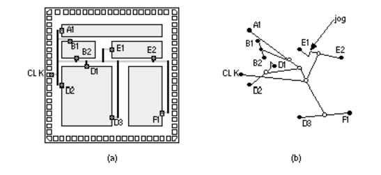
Gate arrays normally use a clock spine (a regular grid), eliminating the need for special routing (see Section 16.1.6, Clock Planning ). The clock distribution grid is designed at the same time as the gate-array base to ensure a minimum clock skew and minimum clock latency given power dissipation and clock buffer area limitations. Cell-based ASICs may use either a clock spine, a clock tree, or a hybrid approach. Figure 17.21 shows how a clock router may minimize clock skew in a clock spine by making the path lengths, and thus net delays, to every leaf node equal using jogs in the interconnect paths if necessary. More sophisticated clock routers perform clock-tree synthesis (automatically choosing the depth and structure of the clock tree) and clock-buffer insertion (equalizing the delay to the leaf nodes by balancing interconnect delays and buffer delays).
FIGURE 17.21 Clock routing. (a) A clock network for the cell-based ASIC from Figure 16.11. (b) Equalizing the interconnect segments between CLK and all destinations (by including jogs if necessary) minimizes clock skew.
The clock tree may contain multiply-driven nodes (more than one active element driving a net). The net delay models that we have used break down in this case
and we may have to extract the clock network and perform circuit simulation, followed by back-annotation of the clock delays to the netlist (for circuit extraction, see Section 17.4 ) and the bus currents to the clock router. The sizes of the clock buses depend on the current they must carry. The limits are set by reliability issues to be discussed next.
Clock skew induced by hot-electron wearout was mentioned in Section 16.1.6,Clock Planning. Another factor contributing to unpredictable clock skew is changes in clock-buffer delays with variations in power-supply voltage due to data-dependent activity. This activity-induced clock skew can easily be larger than the skew achievable using a clock router. For example, there is little point in using software capable of reducing clock skew to less than 100 ps if, due to fluctuations in power-supply voltage when part of the chip becomes active, the clock-network delays change by 200 ps.
The power buses supplying the buffers driving the clock spine carry direct current ( unidirectional current or DC), but the clock spine itself carries alternating current ( bidirectional current or AC). The difference between electromigration failure rates due to AC and DC leads to different rules for sizing clock buses. As we explained in Section 16.1.6, Clock Planning, the fastest way to drive a large load in CMOS is to taper successive stages by approximately e ª 3. This is not necessarily the smallest-area or lowest-power approach, however [ Veendrick, 1984].
17.3.2 Power Routing
Each of the power buses has to be sized according to the current it will carry. Too much current in a power bus can lead to a failure through a mechanism known as electromigration [Young and Christou, 1994]. The required power-bus widths can be estimated automatically from library information, from a separate power simulation tool, or by entering the power-bus widths to the routing software by hand. Many routers use a default power-bus width so that it is quite easy to complete routing of an ASIC without even knowing about this problem.
For a direct current ( DC) the mean time to failure ( MTTF) due to electromigration is experimentally found to obey the following equation:
MTTF = A J 2 exp E / k T , (17.9)
where J is the current density; E is approximately 0.5 eV; k , Boltzmann s constant, is 8.62 ¥ 10 5 eVK 1 ; and T is absolute temperature in kelvins.
There are a number of different approaches to model the effect of an AC component. A typical expression is
A J 2 exp E / k T
MTTF = , (17.10)


1.At 125 °C for unidirectional current. Limits for 110 °C are ¥ 1.5 higher. Limits for 85 °C are ¥ 3 higher. Current limits for bidirectional current are ¥ 1.5 higher than the unidirectional limits.
2.10,000 Å (ten thousand angstroms) = 1 m m.
3.Worst case at 110 °C.

17.4 Circuit Extraction and
DRC
After detailed routing is complete, the exact length and position of each interconnect for every net is known. Now the parasitic capacitance and resistance associated with each interconnect, via, and contact can be calculated. This data is generated by a circuit-extraction tool in one of the formats described next. It is important to extract the parasitic values that will be on the silicon wafer. The mask data or CIF widths and dimensions that are drawn in the logic cells are not necessarily the same as the final silicon dimensions. Normally mask dimensions are altered from drawn values to allow for process bias or other effects that occur during the transfer of the pattern from mask to silicon. Since this is a problem that is dealt with by the ASIC vendor and not the design software vendor, ASIC designers normally have to ask very carefully about the details of this problem.
Table 17.2 shows values for the parasitic capacitances for a typical 1 m m CMOS process. Notice that the fringing capacitance is greater than the parallel-plate (area) capacitance for all layers except poly. Next, we shall describe how the parasitic information is passed between tools.
17.4.1 SPF, RSPF, and DSPF
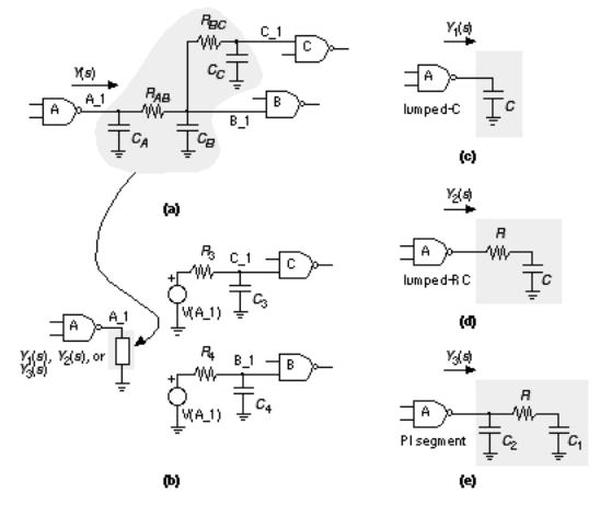
The standard parasitic format ( SPF ) (developed by Cadence [ 1990], now in the hands of OVI) describes interconnect delay and loading due to parasitic resistance and capacitance. There are three different forms of SPF: two of them ( regular SPF and reduced SPF ) contain the same information, but in different formats, and model the behavior of interconnect; the third form of SPF ( detailed SPF ) describes the actual parasitic resistance and capacitance components of a net. Figure 17.22 shows the different types of simplified models that regular and reduced SPF support. The load at the output of gate A is represented by one of three models: lumped-C, lumped-RC, or PI segment. The pin-to-pin delays are modeled by RC delays. You can represent the pin-to-pin interconnect delay by an ideal voltage source, V(A_1) in this case, driving an RC network attached to each input pin. The actual pin-to-pin delays may not be calculated this way, however.
TABLE 17.2 Parasitic capacitances for a typical 1 m m ( l = 0.5 m m) three-level metal CMOS process. 1
Element |
Area / fF m m 2 Fringing / fF m m 1 |
poly (over gate oxide) to |
1.73 |
NA 2 |
||
substrate |
||||
|
|
|
||
poly (over field oxide) to |
0.058 |
0.043 |
||
substrate |
||||
|
|
|
||
m1 to diffusion or poly |
0.055 |
0.049 |
||
m1 to substrate |
0.031 |
0.044 |
||
m2 to diffusion |
0.019 |
0.038 |
||
m2 to substrate |
0.015 |
0.035 |
||
m2 to poly |
0.022 |
0.040 |
||
m2 to m1 |
0.035 |
0.046 |
||
m3 to diffusion |
0.011 |
0.034 |
||
m3 to substrate |
0.010 |
0.033 |
||
m3 to poly |
0.012 |
0.034 |
||
m3 to m1 |
0.016 |
0.039 |
||
m3 to m2 |
0.035 |
0.049 |
||
n+ junction (at 0V bias) |
0.36 |
NA |
||
p+ junction (at 0V bias) |
0.46 |
NA |
||
FIGURE 17.22 The regular and reduced standard parasitic format (SPF) models for interconnect. (a) An example of an interconnect network with fanout. The driving-point admittance of the interconnect network is Y ( s ). (b) The SPF model of the interconnect. (c) The lumped-capacitance interconnect model.
(d) The lumped-RC interconnect model. (e) The PI segment interconnect model (notice the capacitor nearest the output node is labeled C 2 rather than C 1 ). The values of C , R , C 1 , and C 2 are calculated so that Y 1 ( s ), Y 2 ( s ), and Y 3 ( s ) are the first-, second-, and third-order Taylor-series approximations to Y ( s ).
The key features of regular and reduced SPF are as follows:
●The loading effect of a net as seen by the driving gate is represented by choosing one of three different RC networks: lumped-C, lumped-RC, or PI segment (selected when generating the SPF) [ O Brien and Savarino, 1989].
●The pin-to-pin delays of each path in the net are modeled by a simple RC delay (one for each path). This can be the Elmore constant for each path (see Section 17.1.2 ), but it need not be.
Here is an example regular SPF file for just one net that uses the PI segment model shown in Figure 17.22 (e):
#Design Name : EXAMPLE1
#Date : 6 August 1995
#Time : 12:00:00
#Resistance Units : 1 ohms
#Capacitance Units : 1 pico farads
#Syntax :
#N <netName>
#C <capVal>
#F <from CompName> <fromPinName>
#GC <conductance>
#|
#REQ <res>
#GRC <conductance>
#T <toCompName> <toPinName> RC <rcConstant> A <value>
#|
#RPI <res>
#C1 <cap>
#C2 <cap>
#GPI <conductance>
#T <toCompName> <toPinName> RC <rcConstant> A <value>
#TIMING.ADMITTANCE.MODEL = PI
#TIMING.CAPACITANCE.MODEL = PP
N CLOCK
C 3.66
F ROOT Z
RPI 8.85
C1 2.49
C2 1.17
GPI = 0.0
T DF1 G RC 22.20
T DF2 G RC 13.05
This file describes the following:
●The preamble contains the file format.
●This representation uses the PI segment model ( Figure 17.22 e).
●This net uses pin-to-pin timing.
●The driving gate of this net is ROOT and the output pin name is Z .
●The PI segment elements have values: C1 = 2.49 pF, C2 = 1.17 pF, RPI = 8.85 W . Notice the order of C1 and C2 in Figure 17.22 (e). The element
GPI is not normally used in SPF files.
●The delay from output pin Z of ROOT to input pin G of DF1 is 22.20 ns.
●The delay from pin Z of ROOT to pin G of DF2 is 13.05 ns.
The reduced SPF ( RSPF) contains the same information as regular SPF, but uses the SPICE format. Here is an example RSPF file that corresponds to the previous regular SPF example:
*Design Name : EXAMPLE1
*Date : 6 August 1995
*Time : 12:00:00
*Resistance Units : 1 ohms
*Capacitance Units : 1 pico farads *| RSPF 1.0
*| DELIMITER "_"
.SUBCKT EXAMPLE1 OUT IN *| GROUND_NET VSS
*TIMING.CAPACITANCE.MODEL = PP *|NET CLOCK 3.66PF
*|DRIVER ROOT_Z ROOT Z *|S (ROOT_Z_OUTP1 0.0 0.0)
R2 ROOT_Z ROOT_Z_OUTP1 8.85 C1 ROOT_Z_OUTP1 VSS 2.49PF C2 ROOT_Z VSS 1.17PF
*|LOAD DF2_G DF1 G *|S (DF1_G_INP1 0.0 0.0)
E1 DF1_G_INP1 VSS ROOT_Z VSS 1.0 R3 DF1_G_INP1 DF1_G 22.20
C3 DF1_G VSS 1.0PF *|LOAD DF2_G DF2 G *|S (DF2_G_INP1 0.0 0.0)
E2 DF2_G_INP1 VSS ROOT_Z VSS 1.0 R4 DF2_G_INP1 DF2_G 13.05
C4 DF2_G VSS 1.0PF *Instance Section
XDF1 DF1_Q DF1_QN DF1_D DF1_G DF1_CD DF1_VDD DF1_VSS DFF3 XDF2 DF2_Q DF2_QN DF2_D DF2_G DF2_CD DF2_VDD DF2_VSS DFF3 XROOT ROOT_Z ROOT_A ROOT_VDD ROOT_VSS BUF
.ENDS
.END
This file has the following features:
●The PI segment elements ( C1 , C2 , and R2 ) have the same values as the previous example.
●The pin-to-pin delays are modeled at each of the gate inputs with a capacitor of value 1 pF ( C3 and C4 here) and a resistor ( R3 and R4 ) adjusted to give the correct RC delay. Since the load on the output gate is modeled by the PI segment it does not matter what value of capacitance is chosen here.
●The RC elements at the gate inputs are driven by ideal voltage sources ( E1 and E2 ) that are equal to the voltage at the output of the driving gate.
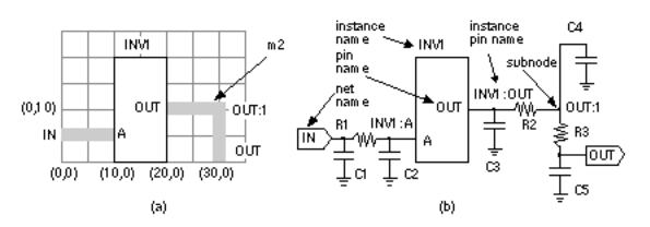
The detailed SPF ( DSPF) shows the resistance and capacitance of each segment in a net, again in a SPICE format. There are no models or assumptions on calculating the net delays in this format. Here is an example DSPF file that describes the interconnect shown in Figure 17.23 (a):
.SUBCKT BUFFER OUT IN
* Net Section
*|GROUND_NET VSS
*|NET IN 3.8E-01PF
*|P (IN I 0.0 0.0 5.0)
*|I (INV1:A INV A I 0.0 10.0 5.0)
C1 IN VSS 1.1E-01PF
C2 INV1:A VSS 2.7E-01PF
R1 IN INV1:A 1.7E00
*|NET OUT 1.54E-01PF
*|S (OUT:1 30.0 10.0)
*|P (OUT O 0.0 30.0 0.0)
*|I (INV:OUT INV1 OUT O 0.0 20.0 10.0)
C3 INV1:OUT VSS 1.4E-01PF
C4 OUT:1 VSS 6.3E-03PF
C5 OUT VSS 7.7E-03PF
R2 INV1:OUT OUT:1 3.11E00
R3 OUT:1 OUT 3.03E00
*Instance Section
XINV1 INV:A INV1:OUT INV
.ENDS
The nonstandard SPICE statements in DSPF are comments that start with '*|' and have the following formats:
*|I(InstancePinName InstanceName PinName PinType PinCap X Y)
*|P(PinName PinType PinCap X Y)
*|NET NetName NetCap
*|S(SubNodeName X Y)
*|GROUND_NET NetName
Figure 17.23 (b) illustrates the meanings of the DSPF terms: InstancePinName , InstanceName , PinName , NetName , and SubNodeName . The PinType is I (for IN) or O (the letter 'O', not zero, for OUT). The NetCap is the total capacitance on each net. Thus for net IN, the net capacitance is
0.38 pF = C1 + C2 = 0.11 pF + 0.27 pF.
This particular file does not use the pin capacitances, PinCap . Since the DSPF represents every interconnect segment, DSPF files can be very large in size (hundreds of megabytes).
FIGURE 17.23 The detailed standard parasitic format (DSPF) for interconnect representation. (a) An example network with two m2 paths connected to a logic cell, INV1. The grid shows the coordinates. (b) The equivalent DSPF circuit corresponding to the DSPF file in the text.
17.4.2 Design Checks
ASIC designers perform two major checks before fabrication. The first check is a design-rule check ( DRC ) to ensure that nothing has gone wrong in the process of assembling the logic cells and routing. The DRC may be performed at two levels. Since the detailed router normally works with logic-cell phantoms, the
first level of DRC is a phantom-level DRC , which checks for shorts, spacing violations, or other design-rule problems between logic cells. This is principally a check of the detailed router. If we have access to the real library-cell layouts (sometimes called hard layout ), we can instantiate the phantom cells and perform a second-level DRC at the transistor level. This is principally a check of the correctness of the library cells. Normally the ASIC vendor will perform this check using its own software as a type of incoming inspection. The Cadence Dracula software is one de facto standard in this area, and you will often hear reference to a Dracula deck that consists of the Dracula code describing an ASIC vendor s design rules. Sometimes ASIC vendors will give their Dracula decks to customers so that the customers can perform the DRCs themselves.
The other check is a layout versus schematic ( LVS ) check to ensure that what is about to be committed to silicon is what is really wanted. An electrical schematic is extracted from the physical layout and compared to the netlist. This closes a loop between the logical and physical design processes and ensures that both are the same. The LVS check is not as straightforward as it may sound, however.
The first problem with an LVS check is that the transistor-level netlist for a large ASIC forms an enormous graph. LVS software essentially has to match this graph against a reference graph that describes the design. Ensuring that every node corresponds exactly to a corresponding element in the schematic (or HDL code) is a very difficult task. The first step is normally to match certain key nodes (such as the power supplies, inputs, and outputs), but the process can very quickly become bogged down in the thousands of mismatch errors that are inevitably generated initially.
The second problem with an LVS check is creating a true reference. The starting point may be HDL code or a schematic. However, logic synthesis, test insertion, clock-tree synthesis, logical-to-physical pad mapping, and several other design steps each modify the netlist. The reference netlist may not be what we wish to fabricate. In this case designers increasingly resort to formal verification that extracts a Boolean description of the function of the layout and compare that to a known good HDL description.
17.4.3 Mask Preparation
Final preparation for the ASIC artwork includes the addition of a maskwork symbol (M inside a circle), copyright symbol (C inside a circle), and company logos on each mask layer. A bonding editor creates a bonding diagram that will show the connection of pads to the lead carrier as well as checking that there are no design-rule violations (bond wires that are too close to each other or that leave the chip at extreme angles). We also add the kerf (which contains alignment marks, mask identification, and other artifacts required in fabrication), the scribe lines (the area where the die will be separated from each other by a diamond saw), and any special hermetic edge-seal structures (usually metal).
The final output of the design process is normally a magnetic tape written in Caltech Intermediate Format ( CIF , a public domain text format) or GDSII Stream (formerly also called Calma Stream, now Cadence Stream), which is a proprietary binary format. The tape is processed by the ASIC vendor or foundry (the fab ) before being transferred to the mask shop .
If the layout contains drawn n -diffusion and p -diffusion regions, then the fab generates the active (thin-oxide), p -type implant, and n -type implant layers. The fab then runs another polygon-level DRC to check polygon spacing and overlap for all mask levels. A grace value (typically 0.01 m m) is included to prevent false errors stemming from rounding problems and so on. The fab will then adjust the mask dimensions for fabrication either by bloating (expanding), shrinking, and merging shapes in a procedure called sizing or mask tooling . The exact procedures are described in a tooling specification . A mask bias is an amount added to a drawn polygon to allow for a difference between the mask size and the feature as it will eventually appear in silicon. The most common adjustment is to the active mask to allow for the bird s beak effect , which causes an active area to be several tenths of a micron smaller on silicon than on the mask.
The mask shop will use e-beam mask equipment to generate metal (usually chromium) on glass masks or reticles . The e-beam spot size determines the resolution of the mask-making equipment and is usually 0.05 m m or 0.025 m m (the smaller the spot size, the more expensive is the mask). The spot size is significant when we break the integer-lambda scaling rules in a deep-submicron process. For example, for a 0.35 m m process ( l = 0.175 m m), a 1.5 l separation is 0.525 m m, which requires more expensive mask-making equipment with a 0.025 m m spot size. For critical layers (usually the polysilicon mask) the mask shop may use optical proximity correction ( OPC ), which adjusts the position of the mask edges to allow for light diffraction and reflection (the deep-UV light used for printing mask images on the wafer has a wavelength comparable to the minimum feature sizes).
1.Fringing capacitances are per isolated line. Closely spaced lines will have reduced fringing capacitance and increased interline capacitance, with increased total capacitance.
2.NA = not applicable.