- •Contents
- •Preface
- •Chapter 1 Introduction (K. Fujimoto)
- •Chapter 2 Small antennas (K. Fujimoto)
- •Chapter 3 Properties of small antennas (K. Fujimoto and Y. Kim)
- •Chapter 4 Fundamental limitation of small antennas (K. Fujimoto)
- •Chapter 5 Subjects related with small antennas (K. Fujimoto)
- •Chapter 6 Principles and techniques for making antennas small (H. Morishita and K. Fujimoto)
- •Chapter 7 Design and practice of small antennas I (K. Fujimoto)
- •Chapter 8 Design and practice of small antennas II (K. Fujimoto)
- •Chapter 9 Evaluation of small antenna performance (H. Morishita)
- •Chapter 10 Electromagnetic simulation (H. Morishita and Y. Kim)
- •Chapter 11 Glossary (K. Fujimoto and N. T. Hung)
- •Acknowledgements
- •1 Introduction
- •2 Small antennas
- •3 Properties of small antennas
- •3.1 Performance of small antennas
- •3.1.1 Input impedance
- •3.1.4 Gain
- •3.2 Importance of impedance matching in small antennas
- •3.3 Problems of environmental effect in small antennas
- •4 Fundamental limitations of small antennas
- •4.1 Fundamental limitations
- •4.2 Brief review of some typical work on small antennas
- •5 Subjects related with small antennas
- •5.1 Major subjects and topics
- •5.1.1 Investigation of fundamentals of small antennas
- •5.1.2 Realization of small antennas
- •5.2 Practical design problems
- •5.3 General topics
- •6 Principles and techniques for making antennas small
- •6.1 Principles for making antennas small
- •6.2 Techniques and methods for producing ESA
- •6.2.1 Lowering the antenna resonance frequency
- •6.2.1.1 SW structure
- •6.2.1.1.1 Periodic structures
- •6.2.1.1.3 Material loading on an antenna structure
- •6.2.2 Full use of volume/space circumscribing antenna
- •6.2.3 Arrangement of current distributions uniformly
- •6.2.4 Increase of radiation modes
- •6.2.4.2 Use of conjugate structure
- •6.2.4.3 Compose with different types of antennas
- •6.2.5 Applications of metamaterials to make antennas small
- •6.2.5.1 Application of SNG to small antennas
- •6.2.5.1.1 Matching in space
- •6.2.5.1.2 Matching at the load terminals
- •6.2.5.2 DNG applications
- •6.3 Techniques and methods to produce FSA
- •6.3.1 FSA composed by integration of components
- •6.3.2 FSA composed by integration of functions
- •6.3.3 FSA of composite structure
- •6.4 Techniques and methods for producing PCSA
- •6.4.2 PCSA employing a high impedance surface
- •6.5 Techniques and methods for making PSA
- •6.5.2 Simple PSA
- •6.6 Optimization techniques
- •6.6.1 Genetic algorithm
- •6.6.2 Particle swarm optimization
- •6.6.3 Topology optimization
- •6.6.4 Volumetric material optimization
- •6.6.5 Practice of optimization
- •6.6.5.1 Outline of particle swarm optimization
- •6.6.5.2 PSO application method and result
- •7 Design and practice of small antennas I
- •7.1 Design and practice
- •7.2 Design and practice of ESA
- •7.2.1 Lowering the resonance frequency
- •7.2.1.1 Use of slow wave structure
- •7.2.1.1.1 Periodic structure
- •7.2.1.1.1.1 Meander line antennas (MLA)
- •7.2.1.1.1.1.1 Dipole-type meander line antenna
- •7.2.1.1.1.1.2 Monopole-type meander line antenna
- •7.2.1.1.1.1.3 Folded-type meander line antenna
- •7.2.1.1.1.1.4 Meander line antenna mounted on a rectangular conducting box
- •7.2.1.1.1.1.5 Small meander line antennas of less than 0.1 wavelength [13]
- •7.2.1.1.1.1.6 MLAs of length L = 0.05 λ [13, 14]
- •7.2.1.1.1.2 Zigzag antennas
- •7.2.1.1.1.3 Normal mode helical antennas (NMHA)
- •7.2.1.1.1.4 Discussions on small NMHA and meander line antennas pertaining to the antenna performances
- •7.2.1.2 Extension of current path
- •7.2.2 Full use of volume/space
- •7.2.2.1.1 Meander line
- •7.2.2.1.4 Spiral antennas
- •7.2.2.1.4.1 Equiangular spiral antenna
- •7.2.2.1.4.2 Archimedean spiral antenna
- •7.2.2.1.4.3.2 Gain
- •7.2.2.1.4.4 Radiation patterns
- •7.2.2.1.4.5 Unidirectional pattern
- •7.2.2.1.4.6 Miniaturization of spiral antenna
- •7.2.2.1.4.6.1 Slot spiral antenna
- •7.2.2.1.4.6.2 Spiral antenna loaded with capacitance
- •7.2.2.1.4.6.3 Archimedean spiral antennas
- •7.2.2.1.4.6.4 Spiral antenna loaded with inductance
- •7.2.2.2 Three-dimensional (3D) structure
- •7.2.2.2.1 Koch trees
- •7.2.2.2.2 3D spiral antenna
- •7.2.2.2.3 Spherical helix
- •7.2.2.2.3.1 Folded semi-spherical monopole antennas
- •7.2.2.2.3.2 Spherical dipole antenna
- •7.2.2.2.3.3 Spherical wire antenna
- •7.2.2.2.3.4 Spherical magnetic (TE mode) dipoles
- •7.2.2.2.3.5 Hemispherical helical antenna
- •7.2.3 Uniform current distribution
- •7.2.3.1 Loading techniques
- •7.2.3.1.1 Monopole with top loading
- •7.2.3.1.2 Cross-T-wire top-loaded monopole with four open sleeves
- •7.2.3.1.3 Slot loaded with spiral
- •7.2.4 Increase of excitation mode
- •7.2.4.1.1 L-shaped quasi-self-complementary antenna
- •7.2.4.1.2 H-shaped quasi-self-complementary antenna
- •7.2.4.1.3 A half-circular disk quasi-self-complementary antenna
- •7.2.4.1.4 Sinuous spiral antenna
- •7.2.4.2 Conjugate structure
- •7.2.4.2.1 Electrically small complementary paired antenna
- •7.2.4.2.2 A combined electric-magnetic type antenna
- •7.2.4.3 Composite structure
- •7.2.4.3.1 Slot-monopole hybrid antenna
- •7.2.4.3.2 Spiral-slots loaded with inductive element
- •7.2.5 Applications of metamaterials
- •7.2.5.1 Applications of SNG (Single Negative) materials
- •7.2.5.1.1.2 Elliptical patch antenna
- •7.2.5.1.1.3 Small loop loaded with CLL
- •7.2.5.1.2 Epsilon-Negative Metamaterials (ENG MM)
- •7.2.5.2 Applications of DNG (Double Negative Materials)
- •7.2.5.2.1 Leaky wave antenna [116]
- •7.2.5.2.3 NRI (Negative Refractive Index) TL MM antennas
- •7.2.6 Active circuit applications to impedance matching
- •7.2.6.1 Antenna matching in transmitter/receiver
- •7.2.6.2 Monopole antenna
- •7.2.6.3 Loop and planar antenna
- •7.2.6.4 Microstrip antenna
- •8 Design and practice of small antennas II
- •8.1 FSA (Functionally Small Antennas)
- •8.1.1 Introduction
- •8.1.2 Integration technique
- •8.1.2.1 Enhancement/improvement of antenna performances
- •8.1.2.1.1 Bandwidth enhancement and multiband operation
- •8.1.2.1.1.1.1 E-shaped microstrip antenna
- •8.1.2.1.1.1.2 -shaped microstrip antenna
- •8.1.2.1.1.1.3 H-shaped microstrip antenna
- •8.1.2.1.1.1.4 S-shaped-slot patch antenna
- •8.1.2.1.1.2.1 Microstrip slot antennas
- •8.1.2.1.1.2.2.2 Rectangular patch with square slot
- •8.1.2.1.2.1.1 A printed λ/8 PIFA operating at penta-band
- •8.1.2.1.2.1.2 Bent-monopole penta-band antenna
- •8.1.2.1.2.1.3 Loop antenna with a U-shaped tuning element for hepta-band operation
- •8.1.2.1.2.1.4 Planar printed strip monopole for eight-band operation
- •8.1.2.1.2.2.2 Folded loop antenna
- •8.1.2.1.2.3.2 Monopole UWB antennas
- •8.1.2.1.2.3.2.1 Binomial-curved patch antenna
- •8.1.2.1.2.3.2.2 Spline-shaped antenna
- •8.1.2.1.2.3.3 UWB antennas with slot/slit embedded on the patch surface
- •8.1.2.1.2.3.3.1 A beveled square monopole patch with U-slot
- •8.1.2.1.2.3.3.2 Circular/Elliptical slot UWB antennas
- •8.1.2.1.2.3.3.3 A rectangular monopole patch with a notch and a strip
- •8.1.2.1.2.3.4.1 Pentagon-shape microstrip slot antenna
- •8.1.2.1.2.3.4.2 Sectorial loop antenna (SLA)
- •8.1.3 Integration of functions into antenna
- •8.2 Design and practice of PCSA (Physically Constrained Small Antennas)
- •8.2.2 Application of HIS (High Impedance Surface)
- •8.2.3 Applications of EBG (Electromagnetic Band Gap)
- •8.2.3.1 Miniaturization
- •8.2.3.2 Enhancement of gain
- •8.2.3.3 Enhancement of bandwidth
- •8.2.3.4 Reduction of mutual coupling
- •8.2.4 Application of DGS (Defected Ground Surface)
- •8.2.4.2 Multiband circular disk monopole patch antenna
- •8.2.5 Application of DBE (Degenerated Band Edge) structure
- •8.3 Design and practice of PSA (Physically Small Antennas)
- •8.3.1 Small antennas for radio watch/clock systems
- •8.3.2 Small antennas for RFID
- •8.3.2.1 Dipole and monopole types
- •8.3.2.3 Slot type antennas
- •8.3.2.4 Loop antenna
- •Appendix I
- •Appendix II
- •References
- •9 Evaluation of small antenna performance
- •9.1 General
- •9.2 Practical method of measurement
- •9.2.1 Measurement by using a coaxial cable
- •9.2.2 Method of measurement by using small oscillator
- •9.2.3 Method of measurement by using optical system
- •9.3 Practice of measurement
- •9.3.1 Input impedance and bandwidth
- •9.3.2 Radiation patterns and gain
- •10 Electromagnetic simulation
- •10.1 Concept of electromagnetic simulation
- •10.2 Typical electromagnetic simulators for small antennas
- •10.3 Example (balanced antennas for mobile handsets)
- •10.3.2 Antenna structure
- •10.3.3 Analytical results
- •10.3.4 Simulation for characteristics of a folded loop antenna in the vicinity of human head and hand
- •10.3.4.1 Structure of human head and hand
- •10.3.4.2 Analytical results
- •11 Glossary
- •11.1 Catalog of small antennas
- •11.2 List of small antennas
- •Index
8.3 Design and practice of PSA |
355 |
|
|
Y
Lb
Wb
Wc X
Lc
Y
|
|
|
|
|
|
|
|
|
|
|
W |
|
|
Via |
|
|
|
|
|
Feed |
X |
|
|
|
|
|
|
|
||||
|
|
|
|
|||||||
|
|
|
|
|
|
|
|
|
|
|
|
|
|
|
|
|
|
|
|
|
|
|
|
|
|
|
|
|
|
|
|
|
|
|
|
|
|
|
|
|
|
|
|
L
Z
h X
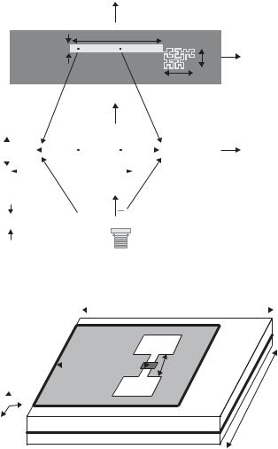
Figure 8.109 Geometry of an IFA top loaded with Hilbert trace [97].
|
|
|
|
|
|
|
|
|
Lg |
|
|
|
|
|
|
|
|
Folded |
|
|
|
|
|
|
|
|
|
|
|
|
|
|
|
||
|
|
|
|
|
|
|
|
|
|
||
|
|
|
|
|
|
patch |
|
g |
|
||
|
|
|
|
W |
|
|
|
|
d |
|
|
|
|
|
|
p |
|
|
|||||
|
|
|
|
|
|
|
|
|
|
|
|
|
y |
|
|
|
b |
|
|
|
|||
|
|
|
|
|
|
|
|
a |
Wg |
|
|
|
|
|
|
|
|
|
|
|
|||
z |
|
x |
|
|
|
L |
|
|
|
||
|
|
|
εs |
hs |
|
Substrate |
|
||||
|
|
|
|
|
|
||||||
|
|
|
|
hI εI |
|
|
|
Body |
Insulator |
|
|
|
|
|
|
|
|
|
|
||||
|
|
|
|
|
|
|
|
|
|
|
Figure 8.110 A folded patch with H-shaped slot loaded with a chip ([99], copyright C 2010 IEEE).
by appropriately designing the size and the shape of the ground plane. With this antenna configuration, antenna performances can be improved, while achieving miniaturization of the antenna.
8.3.2.3Slot type antennas
A slot embedded folded rectangular patch is designed to apply to a wearable UHF RFID sensor tag [99]. Layout of the tag is illustrated in Figure 8.110, where dimensional parameters are also provided. The antenna is essentially a series-fed L-shaped patch and radiates from the open edge of the patch and the slot embedded on the planar element. A sensor chip is located in the middle of the gap between the two slots. Two prototype
356 |
Design and practice of small antennas II |
|
|
Table 8.8 Parameters of two tags [mm] ([99], copyright C 2010 IEEE)
Parameter |
TAG-1 |
TAG-2 |
|
|
|
Wg |
60 |
90 |
W |
60 |
80 |
Lg |
49 |
60 |
L |
49 |
49 |
p |
L/2 |
15 |
a |
8 |
18 |
b |
10 |
9 |
d |
10 |
10 |
g |
3 |
4 |
hs |
4 |
4 |
|
|
|
8 cm
6 cm |
6 cm |
4.9 cm |
6 cm |
9 cm |
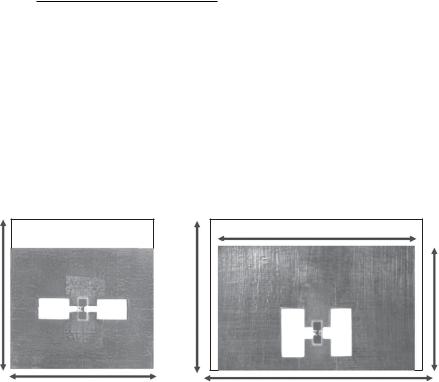
Figure 8.111 Fabricated antenna TAG-1(left) and TAG-2 (right) ([99], copyright C 2010 IEEE).
RFID tags TAG-1 and TAG-2 are fabricated (Figure 8.111) and the parameters are given in Table 8.8. A mechanical motion-vibration sensor is integrated into the antenna structure. This kind of sensor is useful for detection of motion in medical applications, to assist diagnosis of some neurological diseases, involving compulsory arm movements in domestic healthcare, for example to track the behavior of aged persons [99]. The maximum reading range of TAG-1 is 1.5 m by using a short-range reader that emits not more than 0.5 W EIRP at the tag’s microchip power of −30 dBm, while 2.1 m for TAG-2. When a long-range reader (emitting up to 3.2 W EIRP) is used, it increases to 4 m for the TAG-1 and 5.5 m for the TAG-2.
The antenna has a size comparable to a credit card and can be applied to any part of the body. Improvement of the tag is concerned with realization of flexible conformal tags by applying textile technology.
A compact antenna using series OCSRR (Open Complementary Split Ring Resonator) is designed for the passive RFID tags [100]. The OCSRR unit is composed of a circular slot and a conductor loop inserted inside the slot as shown in Figure 8.112(a). Figure 8.112(b) gives the equivalent circuit of the OCSRR unit. The inductance LOCSRR
8.3 Design and practice of PSA |
357 |
|
|
|
|
|
|
|
|
|
|
m |
|
|
|
|
|
|
||
|
|
|
|
|
V |
|
|
|
|
|
|
|
|
|
n |
|
|
|
|
|
|
|
|
|
|
|
|
|
|
|
|||
|
|
|
|
|
|
|
|
|
|
|
|
|
|
|||
|
|
|
|
|
|
|
|
r0 |
|
|
|
|
|
|
||
(a) Port 2 |
|
|
|
f |
|
|
d |
|
|
|
|
|
Port 1 |
|||
|
|
|
|
|
|
|
|
|
|
|||||||
|
|
|
|
|
|
|
|
|
|
|
|
|
||||
|
|
|
|
|
|
|
|
h c |
|
|
g |
|
|
|
|
|
|
|
|
|
|
|
|
|
|
|
|
|
|
|
|||
|
|
|
|
|
|
|
|
|
|
|
|
|||||
|
|
|
|
|
|
|
|
|
|
|
|
|
||||
|
|
|
|
|
|
|
|
|
|
|
|
|
|
|
|
|
|
|
|
|
|
|
|
|
LOCSRR |
|
|
|
|
|
|
||
(b) Port 2 |
|
|
|
|
|
|
|
|
|
|
|
|
|
|
|
Port 1 |
|
|
|
|
|
|
|
|
|
|
|
|
|||||
|
|
|
|
|
|
|
|
|
|
|
|
COCSRR
Figure 8.112 (a) An OCSRR unit and its dimensional parameters and (b) the equivalent circuit ([100], copyright C 2010 IEEE).
|
W |
|
|
|
S |
|
|
y |
k |
H |
|
q |
|||
|
|
||
x |
p |
|
|
|
Port |
|
Figure 8.113 Proposed UHF RFID antenna comprised of series connected OCSRR units ([100], copyright C 2010 IEEE).
is created by the conducting loop between the two inner and outer ring slots and the capacitance COCSRR is between the inner conducting disk and the surrounding outer conducting planes. By connecting OCSRR units in series, and adjusting the size, input resistance and bandwidth can be increased, which is advantageous for matching of small tag antennas that generally have small resistance and high reactance components. Particularly with several units, the inductance becomes four times that of the conventional CSRR and makes for a feasible power harvesting circuit in the passive IC on the RFID tag. The antenna is comprised of four units of OCSRR as shown in Figure 8.113.
The antenna operates at 920 MHz and obtains a maximum reading range of 5.48 m with dimensions of 0.036λ0 × 0.17λ0 (λ0 is the free space wavelength at 920 MHz).
Other examples of RFID tags using slots are a thin L-shaped slot dipole loaded with a meander line at the end of the dipole as shown in Figure 8.114 [101], and a patch antenna on which circular slots are embedded to produce circular polarization as shown in Figure 8.115 [102].
358 |
Design and practice of small antennas II |
|
|
Lv
L1
W1
Lh |
|
|
|
|
L2 |
|
|
|
|
|
|
W2
Figure 8.114 Geometry of a proposed slot dipole antenna loaded with meandered line having RFID chip ([101], copyright C 2010 IEEE).
Asymmetric circular
z
shaped slotted patch
(a) |
Dielectric substrate |
H |
|
|
x |
Ground plane
Coaxial probe
D4 |
y |
D1 |
||
|
S, S |
|
S, S |
|
|
r4 |
|
r1 |
|
|
|
|
|
|
|
x0 |
|
|
x |
(b) |
|
|
|
|
L |
|
|
|
|
|
S, S |
|
S, S |
|
|
r3 |
|
|
|
|
|
r2 |
|
|
|
|
|
|
|
|
|
|
|
|
D3 |
|
|
D2 |
|
|
|
|
Figure 8.115 Unequal size circular slots embedded square patch: (a) cross sectional view and
(b) top view ([102], copyright C 2010 IEEE).