7.2 Design and practice of ESA |
169 |
|
|
as a measure of miniaturization as in the case of narrow-band antennas. Miniaturization in cases of spiral antennas may be interpreted by reduction of the spiral arm length or by lowering operating frequency for the specified gain [51]. In practice, lowering the phase velocity of the wave travelling on the spiral arms can be realized by modifying the spiral arm structure, or by loading either resistance or reactance components on the spiral arms. There is still a need to optimize the antenna structure or way of loading to obtain minimum Q or maximum gain for a wide frequency range with a given antenna size. In this case, techniques for proper matching to keep wideband characteristics are required as well.
7.2.2.1.4.6.1 Slot spiral antenna
The slot spiral antenna has been studied extensively by J. H. Volakis and his colleagues [52–64]. Their work includes development of design algorithms to optimize the antenna geometry, feed, loading, and so forth, and demonstrates techniques of miniaturization and practical models. As spiral antennas have inherently wide bandwidth, miniaturization should be realized without losing the initial wideband characteristics. Loading of resistance, reactive components or materials is a common method for miniaturizing antennas. When applying the loading method to spiral antennas, specific care must be taken to keep wideband characteristics. Practical methods are, for example, modifying antenna structure by meandering or coiling, using dielectric materials in superstrate as well as substrate, and so forth. Wideband matching can be done, for instance, by tapering resistive loading on the spiral arms, by infinite coaxial balun along with spiral arms, by the broadband hybrid, and so forth. Since the slot radiates to both front and back sides normally to the spiral surface, the antenna is often placed on a thin cavity to produce unidirectional radiation, which is desired in many cases of practical operation. The spiral slot structure has a feature that is different from usual spiral of conducting arms; since the source of radiation is magnetic current, the spiral element can be placed close to the metallic ground plane that attributes the positive image effect, resulting in increase of the antenna gain and thinning the antenna structure as well. Some examples are introduced below.
An example of a slot spiral antenna is illustrated in Figure 7.127 [50], which shows the radiating slot spiral antenna; (a) cross section, (b) underside view, and (c) top view with microstrip balun. The antenna type is an Archimedean spiral, which is mathematically described as r = aθ + b, where r is the radian length from the origin, a is the spiral growth rate, θ is the angular position, and b is the initial radial offset from the origin. Geometries of the antenna are: a = 0.28 cm/radian, θ is in a range from 0.0 to 24.5 radians, b = 0, the maximum diameter dmax of the radiating slot is 14.5 cm, and the slot width w = 0.762 mm. The substrate εr = 3.38 and the thickness of the substrate is 7.62 mm. The balun is constituted with microstrip line, which is placed on the metal part of the spiral toward the origin (center) of the spiral, using the radiating slot as its ground plane as Figure 7.127(a) and (c), respectively, show. At the periphery of the spiral, a coaxial connector is soldered to the microstrip line, and at the center of the spiral, the end of the microstrip line is shorted across the slot line to feed the slot. Termination of the slot
170 |
Design and practice of small antennas I |
|
|
Balun Slot spiral Feed
(a)
|
Cavity |
|
|
|
|
Substrate |
Cavity bottom |
|
|
|
|
Microstrip |
Microstrip-slot |
|
Coaxial-microstrip |
Microstrip-slot |
transition |
||
infinite |
||||
transition |
transition |
region |
||
balun |
||||
region |
region |
|
||
|
|
(b) |
(c) |
Slotline |
|
Thick-film |
Coaxial-microstrip |
slot termination |
transition region |
Figure 7.127 Geometry of Archimedean spiral antenna backed with cavity: (a) cross section view,
(b) underside view, and (c) top view ([51], copyright C 2001 IEEE).
Beginning of |
|
termination |
Chip resistor |
|
End of termination
Figure 7.128 Slot spiral termination with thick-film resistors ([51], copyright C 2001 IEEE).
is done by loading resistances on the slot line, forming an impedance transformer between the antenna impedance and the feed so as to ensure wideband characteristics and achieve desired axial ratio. The termination is implemented by using 60resistors, distributed equally along the overall transformer length. Figure 7.128 illustrates the implemented termination by using the thick-film resistor [54]. The diameter of the cavity is 14.9 cm, which can just accommodate the slots and the termination resistors. The depth D of the cavity is set by the maximum desired frequency of the antenna, and at that point it

7.2 Design and practice of ESA |
171 |
|
|
ε1 |
W |
T |
εr |
|
t |
D |
|
|
ε = 1 |
|
|
|
d |
|
D = 1.266 cm, d = 14.5 cm, t = 0.508 mm, |
|
T = 0 cm, 60 resistors/arm, ε1 = 1, |
|
w = 0.762 mm, εr = (3.38,–0.009). |
|
Figure 7.129 Antenna geometry cross section, which shows loading with substrate of dielectric constant εr and superstrate of dielectric constant ε1 ([51], copyright C 2001 IEEE).
should be less than λhighest/4 to prevent destructive interference. The minimum depth of the cavity is determined by the slot width w and substrate dielectric constant εr. The actual depth of the cavity used is 6.35 mm (λlowest/60).
7.2.2.1.4.6.2 Spiral antenna loaded with capacitance
This spiral antenna is miniaturized by either capacitive loading or inductive loading on the spiral arms. The capacitive loading is implemented by applying dielectric substrate and/or superstrate to the spiral surface. Figure 7.129 shows cross section of the antenna geometry in the cavity when a dielectric substrate with εr, having the thickness T, or a dielectric superstrate with ε1, having thickness t, is used. MFsm (near-field miniaturization factor) is evaluated by taking the electrical lengths of spiral arms for various loadings θ loaded and θ unloaded, given in [51] as
MFsm = θloaded/θunloaded. (7.66)
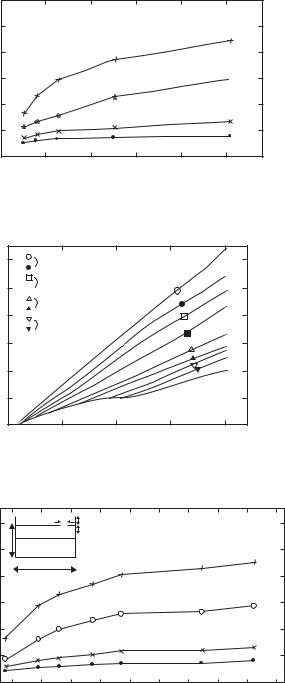
Figure 7.130 shows MFsm as a function of substrate thickness with four values of εr. The phase progression on the slot line when dielectric superstrate (with ε1 = εr) is added on the slot line is depicted in Figure 7.131, which shows variation of phase angle with respect to the slot line length for two different thickness t (0 cm with white points, and 0.0508 cm with black points) and four different εr (2.2, 3.38, 6.15, and 10.2) of the superstrate. This figure clearly gives an evidence of increase in the electrical length of the slot with increase in εr of the superstrate. Figure 7.132 gives near-field miniaturization factor MFsm with respect to the superstrate thickness t for four values of εr (from 2.2 to 10.2). Gain of this antenna is about 0 dB around 1 GHz.
Miniaturization can also be done by loading either capacitive or inductive components on the slot line that increases electrical length of the slot line and thus lowers the operating frequency [58–63].