


8Design and practice of small antennas II
8.1FSA (Functionally Small Antennas)
8.1.1Introduction
A Functionally Small Antenna (FSA) is an antenna system that has enhanced or improved performances without increasing the antenna dimensions. The FSA is constituted by
(1) integrating or combining either radiating or non-radiating components into an antenna system so as to improve or enhance the antenna performance, and (2) adding some function to an antenna so that the antenna will perform with newly added function. The Functionally Small Antenna system is not necessarily dimensionally small; however, it can be referred to equivalently as a small antenna, because enhanced performances or added functions compare to a larger antenna that could not be accomplished otherwise without enlarging the antenna dimensions.
Components to be integrated or combined into an antenna structure are electronic devices (either passive or active). There are many cases where antenna elements, regardless of either linear or planar, are combined with other antenna elements to constitute an integrated antenna. An antenna composed with integrated structure is referred to as an Integrated Antenna System (IAS). An IAS containing active components is referred to as an active IAS.
8.1.2Integration technique
There is a three-fold benefit of the integration techniques: (a) enhancement/improvement of antenna performances; (b) reduction of antenna dimensions; and (c) addition of some functions to an antenna system. The design target pertaining to (a) is enhancement/ improvement of bandwidth, including multiband as well as wideband performance, and of gain or efficiency. Factors in (b) lead to miniaturization, and those in (c) include addition of functions such as variable tuning facility, reconfigurable operation as well as amplification, frequency conversion, oscillation, and so forth, all integrated into an antenna system.
8.1.2.1Enhancement/improvement of antenna performances
When designing a small antenna, to keep the bandwidth at least the same or increase it without degradation in gain and efficiency is the prime factor to consider. The integration technique may be employed as one of the most useful approaches for this purpose.
8.1 FSA (Functionally Small Antennas) |
269 |
|
|
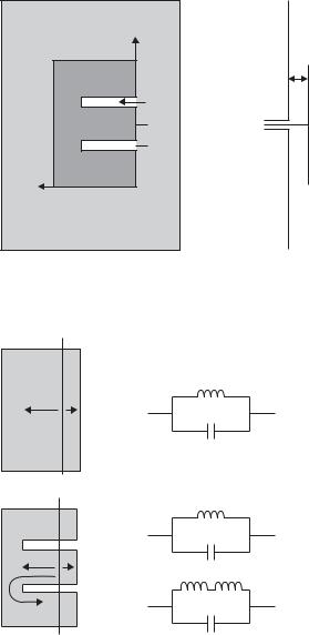
and the two equivalent LC circuits; one for the center part of the patch and another for the two side parts of the E-shaped patch. On the ordinary rectangular patch, current J flows from the feed point to the top and bottom edges of the patch and these current path lengths determine the inductance L and the capacitance C, as Figure 8.2(a) shows. On the other hand, a current on the E-shaped patch flows on the center part of the E-shape like an ordinary patch and other current flows into side parts of the E-shape taking the roundabout path, as Figure 8.2(b) shows. The center part of the E-shape patch can be modeled by a simple LC resonant circuit like the ordinary patch circuit, while the side part of the E-shape patch is modeled by a circuit with an additional series inductance Ls to L as shown in Figure 8.2(b). Hence, the equivalent circuit of the side part resonates at lower frequency than that of the center part. This means that a model of an E-shaped patch antenna changes from a single-resonance circuit to a dual-resonance circuit. Thus, coupling together of these circuits leads to wideband performance.
Essential parameters in the design of an E-shaped patch antenna are slot length Ls, slot position Ps, and slot width Ws. The slot length Ls is the important factor to characterize the resonance frequency; when the Ls is too short, the antenna has only one resonance frequency. As Ls increases, another lower resonance frequency appears. The longer Ls becomes, the lower the second resonance frequency will be. Ps is a parameter that can adjust matching conditions properly. When Ps becomes somewhat larger, the two resonance frequencies become distinct and a wideband match is obtained. However, as Ps further increases, the S11 between two resonance frequencies is larger than –10 dB. Then the antenna does not perform as a wideband antenna, but as a dual-band antenna. The third parameter Ws is a useful parameter to adjust coupling and achieve good matching.
An E-shaped patch antenna was developed for use in wireless communications operating at 1.9–2.4 GHz [1]. The antenna geometrical parameters are L = 70, W = 50, h = 15, Xf = 35, Yf = 6, Ls = 40, Ws = 6, and Ps = 10, where dimensions are all in mm. Calculated and measured S11 are shown in Figure 8.3, in which S11 of two other ordinary patch antennas (without slots) are provided for comparison. They have the same height and width as the E-shaped patch antenna, but the narrow patch antenna is one having the same length as the middle part of the E-shaped patch, and has a bandwidth about only 10%, while the wide patch is one with the same length as the E-shaped patch antenna and does not match well to 50 . On the contrary, the E-shaped patch antenna has shown resonance at two frequencies, 1.9 GHz and 2.4 GHz, and the bandwidth is 30.3%.
It should be noted that the ground plane (GP) often becomes a critical factor when a platform to mount an antenna is small. In this example [1], the size of GP is chosen to be 14 × 21 cm, which is about eight times that of the patch size. By observing the current distributions on the GP obtained by calculation, most currents flow under the patch, but a larger area is required for lower frequencies than higher frequencies. It was concluded that a 1λ (1.9 GHz) square plate is sufficient for proper operation of the antenna.
Directivity of the antenna is calculated to be 8.5 dB at 2.4 GHz and 6.7 dB at 1.9 GHz. The measured radiation patterns agree well with the calculated results. In the E-plane, the 3-dB beamwidth is 42◦ at 2.4 GHz and 63◦ at 1.9 GHz. The peak cross polarization at 2.4 GHz is –25 dB, and is lower than –15 dB at 1.9 GHz. In the H-plane, the radiation patterns are similar to those of the E-plane, and the 3-dB beamwidth is 60◦ at both
270 |
Design and practice of small antennas II |
|
|
0
–5
–10
S11 (dB)
–15
–20
E–shaped, measured E–shaped, calculated Narrow patch, calculated Wide patch, calculated
–25 |
2 |
2.5 |
3 |
1.5 |
Frequency (GHz)
Figure 8.3 S11 of the E-shaped patch antenna, compared with simple patch without slots ([1], copyright C 2001 IEEE).
frequencies. The peak cross polarization is –7 dB at 50◦, a rather high level that is due to the leaky radiation of the slots.
Another example shown in [1] is a wider band that was achieved by adjusting the parameters of the slots and the feeding point of an E-shaped patch antenna. The antenna has two distinct resonant frequencies at 2.12 GHz and 2.66 GHz and the frequency band ranges from 2.05–2.64 GHz, resulting in bandwidth as wide as 32.3%.
Another example of an E-shaped patch antenna introduced in [2] is designed to operate in the 800 MHz band and has wide bandwidth of 164 MHz. In order to obtain wider bandwidth, an LC circuit comprised of a small spiral, which produces an inductance, and a circular plate, which introduces a capacitance to compensate the inductance of the spiral and the feed line, thus producing a new resonance, is integrated into the feed circuit. This resonance frequency is very close to that of the E-shaped patch and thus wider bandwidth can be achieved.
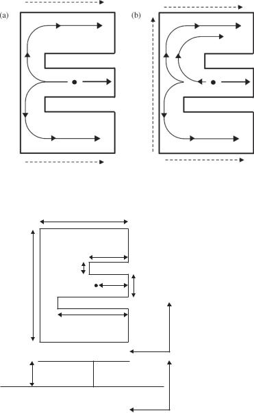
An E-shaped patch antenna radiates a linearly polarized wave when currents on both side parts of the E-shaped surface are the same; however, when they are different as shown in Figure 8.4 [3], elliptically or circularly polarized (CP) waves are radiated. As can be observed in the figure, when the slot length varies, currents flowing on both sides of the E-shaped surface become unbalanced. When by this means, the x-directed current is made equal in magnitude to the y-directed current with a 90-degree phase difference,
8.1 FSA (Functionally Small Antennas) |
271 |
|
|
Figure 8.4 Current flow across the E-shaped patch: (a) symmetrical flow and (b) asymmetrical flow ([2, 3], copyright C 2010 IEEE).
(a) |
L |
|
|
|
Ls1 |
|
Ws |
W |
F |
P |
|
|
x |
|
Ls2 |
|
y |
(b) |
z |
|
|
h |
|
|
y |
Figure 8.5 Geometry of a patch antenna with slots of different length: (a) top view and (b) side view ([2, 3], copyright C 2010 IEEE).
an E-shaped antenna radiates a CP wave. The parameters to be considered in the design of a CP antenna are: each length of its two slots, Ls1 and Ls2; the slot width Ws; the separation P between two slots and the location of the feed point F with a given patch size; length L; and width W . The antenna geometry is shown in Figure 8.5, (a) top and
(b) side views.

272Design and practice of small antennas II
Table 8.1 Dimensions of circularly polarized E-shaped patch
[mm]([3], copyright C 2010 IEEE)
εr |
h |
W |
L |
Ws |
Ls1 |
Ls2 |
P |
F |
1 |
10 |
77 |
47.5 |
7 |
19 |
44.5 |
14 |
17 |
2.2 |
6.7 |
63 |
33.5 |
4 |
27 |
6 |
20 |
10 |
|
|
|
|
|
|
|
|
|
The design procedure starts with an E-shape having the same length Ls1 and Ls2, then shortens either Ls1 or Ls2 to obtain circular polarization. Next change the probe position F to have improved AR (axial ratio) and S11, and align Ls2 or Ls1 for fine enhancement of AR as well as alignment with the S11 band. Finally, the design procedure ends when desired CP is obtained, otherwise, iterate back to the second step and repeat the steps again to satisfy the requirements. In the second step, make Ls1 shorter with Ls2 fixed, if left-handed (LH) CP is required, whereas if right-handed (RH) CP is desired, follow the opposite procedure. When making Ls1 shorter, the resonance frequency becomes higher and at the same time AR decreases from larger values showing linear polarization to smaller values to show CP, as the Ls1 changes electrical path length of the x-directed current. In this process, there is a state where Ls1 takes optimum values for the minimum AR as the phase difference between orthogonal currents approaches 90 degrees. Beyond this critical value, the phase difference between the orthogonal currents departs from 90 degrees. The design goal is to achieve desired AR bandwidth, which is defined as the frequency range across the 3-dB AR level, and to obtain required impedance and AR bandwidth together.
A CP E-shaped patch antenna to cover the IEEE 802.11b/g band (2.4–2.5 GHz) is proposed and antenna performances are introduced [3]. Dimensions of the antenna are provided in Table 8.1 (in mm). The metallic patch is fabricated via milling a thin copperclad substrate, which has εr = 2.2 and thickness of 0.787 mm. The patch is mounted above a ground plane of 200 × 95 mm by using a via of 0.75 mm radius, which is connected to the center pin of the 50connector. Simulated and measured S11 are shown in Figure 8.6. The measured impedance bandwidth is 9.27% (2.34–2.57 GHz) while simulated bandwidth is 10.27% (2.31–2.57 GHz). AR obtained by simulation and measurement is given in Figure 8.7, by which AR bandwidth is observed to be 8.1% (2.28–2.45 GHz) in simulation, while 16% (2.3–2.7 GHz) in measurement. Bandwidths for S11 and AR overlap in the range 2.34–2.57 GHz (9.27%). The maximum measured gain is 8.3 dBi with 15.5% 3-dB bandwidth. This can be observed in Figure 8.8, which depicts gain with respect to frequency. The bandwidth common to all of AR, gain, and S11 is 9.27%.
The E-shaped patch antenna may have great potential to be applied in various purposes such as reconfigurable antenna, diversity antenna, etc. For example, implementation of a reconfigurable antenna becomes feasible by inserting RF switches in appropriate locations across each slot and turning them on or off to make the two slot lengths unequal, thereby producing CP radiation as a consequence.


 2 2.1 2.2 2.3 2.4 2.5 2.6 2.7 2.8 2.9 3


 2 2.1 2.2 2.3 2.4 2.5 2.6 2.7 2.8 2.9 3


 2 2.1 2.2 2.3 2.4 2.5 2.6 2.7 2.8 2.9 3