- •Contents
- •Preface
- •Chapter 1 Introduction (K. Fujimoto)
- •Chapter 2 Small antennas (K. Fujimoto)
- •Chapter 3 Properties of small antennas (K. Fujimoto and Y. Kim)
- •Chapter 4 Fundamental limitation of small antennas (K. Fujimoto)
- •Chapter 5 Subjects related with small antennas (K. Fujimoto)
- •Chapter 6 Principles and techniques for making antennas small (H. Morishita and K. Fujimoto)
- •Chapter 7 Design and practice of small antennas I (K. Fujimoto)
- •Chapter 8 Design and practice of small antennas II (K. Fujimoto)
- •Chapter 9 Evaluation of small antenna performance (H. Morishita)
- •Chapter 10 Electromagnetic simulation (H. Morishita and Y. Kim)
- •Chapter 11 Glossary (K. Fujimoto and N. T. Hung)
- •Acknowledgements
- •1 Introduction
- •2 Small antennas
- •3 Properties of small antennas
- •3.1 Performance of small antennas
- •3.1.1 Input impedance
- •3.1.4 Gain
- •3.2 Importance of impedance matching in small antennas
- •3.3 Problems of environmental effect in small antennas
- •4 Fundamental limitations of small antennas
- •4.1 Fundamental limitations
- •4.2 Brief review of some typical work on small antennas
- •5 Subjects related with small antennas
- •5.1 Major subjects and topics
- •5.1.1 Investigation of fundamentals of small antennas
- •5.1.2 Realization of small antennas
- •5.2 Practical design problems
- •5.3 General topics
- •6 Principles and techniques for making antennas small
- •6.1 Principles for making antennas small
- •6.2 Techniques and methods for producing ESA
- •6.2.1 Lowering the antenna resonance frequency
- •6.2.1.1 SW structure
- •6.2.1.1.1 Periodic structures
- •6.2.1.1.3 Material loading on an antenna structure
- •6.2.2 Full use of volume/space circumscribing antenna
- •6.2.3 Arrangement of current distributions uniformly
- •6.2.4 Increase of radiation modes
- •6.2.4.2 Use of conjugate structure
- •6.2.4.3 Compose with different types of antennas
- •6.2.5 Applications of metamaterials to make antennas small
- •6.2.5.1 Application of SNG to small antennas
- •6.2.5.1.1 Matching in space
- •6.2.5.1.2 Matching at the load terminals
- •6.2.5.2 DNG applications
- •6.3 Techniques and methods to produce FSA
- •6.3.1 FSA composed by integration of components
- •6.3.2 FSA composed by integration of functions
- •6.3.3 FSA of composite structure
- •6.4 Techniques and methods for producing PCSA
- •6.4.2 PCSA employing a high impedance surface
- •6.5 Techniques and methods for making PSA
- •6.5.2 Simple PSA
- •6.6 Optimization techniques
- •6.6.1 Genetic algorithm
- •6.6.2 Particle swarm optimization
- •6.6.3 Topology optimization
- •6.6.4 Volumetric material optimization
- •6.6.5 Practice of optimization
- •6.6.5.1 Outline of particle swarm optimization
- •6.6.5.2 PSO application method and result
- •7 Design and practice of small antennas I
- •7.1 Design and practice
- •7.2 Design and practice of ESA
- •7.2.1 Lowering the resonance frequency
- •7.2.1.1 Use of slow wave structure
- •7.2.1.1.1 Periodic structure
- •7.2.1.1.1.1 Meander line antennas (MLA)
- •7.2.1.1.1.1.1 Dipole-type meander line antenna
- •7.2.1.1.1.1.2 Monopole-type meander line antenna
- •7.2.1.1.1.1.3 Folded-type meander line antenna
- •7.2.1.1.1.1.4 Meander line antenna mounted on a rectangular conducting box
- •7.2.1.1.1.1.5 Small meander line antennas of less than 0.1 wavelength [13]
- •7.2.1.1.1.1.6 MLAs of length L = 0.05 λ [13, 14]
- •7.2.1.1.1.2 Zigzag antennas
- •7.2.1.1.1.3 Normal mode helical antennas (NMHA)
- •7.2.1.1.1.4 Discussions on small NMHA and meander line antennas pertaining to the antenna performances
- •7.2.1.2 Extension of current path
- •7.2.2 Full use of volume/space
- •7.2.2.1.1 Meander line
- •7.2.2.1.4 Spiral antennas
- •7.2.2.1.4.1 Equiangular spiral antenna
- •7.2.2.1.4.2 Archimedean spiral antenna
- •7.2.2.1.4.3.2 Gain
- •7.2.2.1.4.4 Radiation patterns
- •7.2.2.1.4.5 Unidirectional pattern
- •7.2.2.1.4.6 Miniaturization of spiral antenna
- •7.2.2.1.4.6.1 Slot spiral antenna
- •7.2.2.1.4.6.2 Spiral antenna loaded with capacitance
- •7.2.2.1.4.6.3 Archimedean spiral antennas
- •7.2.2.1.4.6.4 Spiral antenna loaded with inductance
- •7.2.2.2 Three-dimensional (3D) structure
- •7.2.2.2.1 Koch trees
- •7.2.2.2.2 3D spiral antenna
- •7.2.2.2.3 Spherical helix
- •7.2.2.2.3.1 Folded semi-spherical monopole antennas
- •7.2.2.2.3.2 Spherical dipole antenna
- •7.2.2.2.3.3 Spherical wire antenna
- •7.2.2.2.3.4 Spherical magnetic (TE mode) dipoles
- •7.2.2.2.3.5 Hemispherical helical antenna
- •7.2.3 Uniform current distribution
- •7.2.3.1 Loading techniques
- •7.2.3.1.1 Monopole with top loading
- •7.2.3.1.2 Cross-T-wire top-loaded monopole with four open sleeves
- •7.2.3.1.3 Slot loaded with spiral
- •7.2.4 Increase of excitation mode
- •7.2.4.1.1 L-shaped quasi-self-complementary antenna
- •7.2.4.1.2 H-shaped quasi-self-complementary antenna
- •7.2.4.1.3 A half-circular disk quasi-self-complementary antenna
- •7.2.4.1.4 Sinuous spiral antenna
- •7.2.4.2 Conjugate structure
- •7.2.4.2.1 Electrically small complementary paired antenna
- •7.2.4.2.2 A combined electric-magnetic type antenna
- •7.2.4.3 Composite structure
- •7.2.4.3.1 Slot-monopole hybrid antenna
- •7.2.4.3.2 Spiral-slots loaded with inductive element
- •7.2.5 Applications of metamaterials
- •7.2.5.1 Applications of SNG (Single Negative) materials
- •7.2.5.1.1.2 Elliptical patch antenna
- •7.2.5.1.1.3 Small loop loaded with CLL
- •7.2.5.1.2 Epsilon-Negative Metamaterials (ENG MM)
- •7.2.5.2 Applications of DNG (Double Negative Materials)
- •7.2.5.2.1 Leaky wave antenna [116]
- •7.2.5.2.3 NRI (Negative Refractive Index) TL MM antennas
- •7.2.6 Active circuit applications to impedance matching
- •7.2.6.1 Antenna matching in transmitter/receiver
- •7.2.6.2 Monopole antenna
- •7.2.6.3 Loop and planar antenna
- •7.2.6.4 Microstrip antenna
- •8 Design and practice of small antennas II
- •8.1 FSA (Functionally Small Antennas)
- •8.1.1 Introduction
- •8.1.2 Integration technique
- •8.1.2.1 Enhancement/improvement of antenna performances
- •8.1.2.1.1 Bandwidth enhancement and multiband operation
- •8.1.2.1.1.1.1 E-shaped microstrip antenna
- •8.1.2.1.1.1.2 -shaped microstrip antenna
- •8.1.2.1.1.1.3 H-shaped microstrip antenna
- •8.1.2.1.1.1.4 S-shaped-slot patch antenna
- •8.1.2.1.1.2.1 Microstrip slot antennas
- •8.1.2.1.1.2.2.2 Rectangular patch with square slot
- •8.1.2.1.2.1.1 A printed λ/8 PIFA operating at penta-band
- •8.1.2.1.2.1.2 Bent-monopole penta-band antenna
- •8.1.2.1.2.1.3 Loop antenna with a U-shaped tuning element for hepta-band operation
- •8.1.2.1.2.1.4 Planar printed strip monopole for eight-band operation
- •8.1.2.1.2.2.2 Folded loop antenna
- •8.1.2.1.2.3.2 Monopole UWB antennas
- •8.1.2.1.2.3.2.1 Binomial-curved patch antenna
- •8.1.2.1.2.3.2.2 Spline-shaped antenna
- •8.1.2.1.2.3.3 UWB antennas with slot/slit embedded on the patch surface
- •8.1.2.1.2.3.3.1 A beveled square monopole patch with U-slot
- •8.1.2.1.2.3.3.2 Circular/Elliptical slot UWB antennas
- •8.1.2.1.2.3.3.3 A rectangular monopole patch with a notch and a strip
- •8.1.2.1.2.3.4.1 Pentagon-shape microstrip slot antenna
- •8.1.2.1.2.3.4.2 Sectorial loop antenna (SLA)
- •8.1.3 Integration of functions into antenna
- •8.2 Design and practice of PCSA (Physically Constrained Small Antennas)
- •8.2.2 Application of HIS (High Impedance Surface)
- •8.2.3 Applications of EBG (Electromagnetic Band Gap)
- •8.2.3.1 Miniaturization
- •8.2.3.2 Enhancement of gain
- •8.2.3.3 Enhancement of bandwidth
- •8.2.3.4 Reduction of mutual coupling
- •8.2.4 Application of DGS (Defected Ground Surface)
- •8.2.4.2 Multiband circular disk monopole patch antenna
- •8.2.5 Application of DBE (Degenerated Band Edge) structure
- •8.3 Design and practice of PSA (Physically Small Antennas)
- •8.3.1 Small antennas for radio watch/clock systems
- •8.3.2 Small antennas for RFID
- •8.3.2.1 Dipole and monopole types
- •8.3.2.3 Slot type antennas
- •8.3.2.4 Loop antenna
- •Appendix I
- •Appendix II
- •References
- •9 Evaluation of small antenna performance
- •9.1 General
- •9.2 Practical method of measurement
- •9.2.1 Measurement by using a coaxial cable
- •9.2.2 Method of measurement by using small oscillator
- •9.2.3 Method of measurement by using optical system
- •9.3 Practice of measurement
- •9.3.1 Input impedance and bandwidth
- •9.3.2 Radiation patterns and gain
- •10 Electromagnetic simulation
- •10.1 Concept of electromagnetic simulation
- •10.2 Typical electromagnetic simulators for small antennas
- •10.3 Example (balanced antennas for mobile handsets)
- •10.3.2 Antenna structure
- •10.3.3 Analytical results
- •10.3.4 Simulation for characteristics of a folded loop antenna in the vicinity of human head and hand
- •10.3.4.1 Structure of human head and hand
- •10.3.4.2 Analytical results
- •11 Glossary
- •11.1 Catalog of small antennas
- •11.2 List of small antennas
- •Index
8.1 FSA (Functionally Small Antennas) |
313 |
|
|
y |
|
|
y |
|
(xN, yN) |
|
|
w5 |
|
|
|
|
(x2, y2) |
|
|
w1 |
(x1, y1) |
w1 |
|
|
|
|
|
w4 |
|
|
|
w3 |
w6 |
|
w6 |
z |
x |
x |
z |
|
w2 |
|
w2 |
(a) |
|
|
(b) |
Figure 8.58 Spline curved planar monopole antenna, indicating points for defining spline;
(a) front view and (b) back view ([38a], copyright C 2007 IEEE).
8.1.2.1.2.3.2.2 Spline-shaped antenna
A spline-shaped UWB antenna was synthesized [38a]. An innovative design approach based on the use of a spline description is applied to create a novel UWB antenna geometry. It is also used for formulation of the synthesis in terms of return loss at the input port and coupling properties of a system with identical antennas modeling the UWB communication. A suitable implementation of the PSO (Particle Swarm Optimization) has been integrated with spline-based shape generator and a MoM-based electromagnetic simulator.
The representative parameters to be optimized are shown in Figure 8.58, where the coordinates of the nth control points to be determined by the optimization are given as Pn (xn, yn), taken on the coordinate (x, y). Here n = 1,2, . . . N; N being the total number of the control points used to describe the antenna geometry.
The antenna is printed on the front side of the substrate (thickness 0.78 mm and εr = 3.38), having length w1 = 69.2 mm and half-width w2 = 10 mm, and the ground plane of length w6 = 51 mm is printed on the lower part of the back side of the substrate. The antenna geometry is characterized by the array of geometric variables
X = {(xn , yn ), n = 1, . . . , N ; w1, w2, . . . , w6}. |
(8.2) |
In the UWB communication system, impedance matching and distortionless conditions for the UWB bandwidth are imposed as the electrical constraints. As for the impedance matching over the UWB bandwidth,
|S11( f )| ≤ −10 dB.
314 |
Design and practice of small antennas II |
|
|
(a) |
(b) |
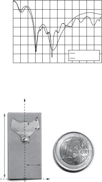
Figure 8.59 A proto-type dongle antenna: (a) front view and (b) back view ([38a], copyrightC 2007 IEEE).
And for the condition of distortionless system, the antenna is required to satisfy a condition pertaining to the magnitude of S21, |S21 (f)| to be
|S21| ≤ 6 dB.
And the group delay τ g,
τg ≤ 1 ns.
Here |S21| and τ g, respectively, denote the maximum variation in the whole frequency band of |S21| and τ g.
The antenna is required to be placed on the platform of the size 100 × 60 (in mm). By the optimization, coordinates of the control points are; p1 (6.9, 50.6), p2 (9, 55.5),
p3 (7, 62.7), p4 (2.7, 66.3), and p5 (1.9, 61.8) all in mm. As for the feeding line, w4 = 5.4, and w3 and w5, which define the range of contour variations along the y-axis, are 51.6 and 56, respectively. A prototype antenna is illustrated in Figure 8.59, (a) front view and (b) back view. Simulated and measured return loss is shown in Figure 8.60.
The spline-shaped UWB antenna is applied to integrate in a wireless USB (Universal Serial Bus) dongle [38b]. It has a miniaturized planar structure with maximum extension 39.2 × 19.2, within which the radiator occupies only an area of 16.2 × 19.2 mm. The antenna is printed on a two-sided dielectric substrate (εr = 3.38 and thickness 0.78 mm) and the geometry is defined by the set of values of the descriptive parameters; ϕ1 (length of the substrate) = 39.2, ϕ2 (half-width of the substrate) = 9.6, ϕ3 (half width of the feeding point) = 2.1, and ϕ4 (length of the ground plane) = 23.0 (in mm). Antenna geometry is determined by the spline-description, giving control points on the (x, y)
8.1 FSA (Functionally Small Antennas) |
315 |
|
|
|S11| (dB)
0 |
|
|
|
|
|
|
|
|
|
|
|
|
|
−5 |
|
|
|
|
|
|
|
|
|
|
|
|
|
−10 |
|
|
|
|
|
|
|
|
|
|
|
|
|
−15 |
|
|
|
|
|
|
|
|
|
|
|
|
|
−20 |
|
|
|
|
|
|
|
|
|
|
|
|
|
−25 |
|
|
|
|
|
|
|
|
|
|
|
|
|
−30 |
|
|
|
|
|
|
|
|
Simulated data |
|
|||
−35 |
|
|
|
|
|
|
|
|
Measured data |
|
|||
2 |
3 |
4 |
5 |
6 |
7 |
8 |
9 |
10 |
11 |
12 |
13 |
||
1 |
Frequency (GHz)
Figure 8.60 Simulated and measured return loss of the dongle antenna ([38a], copyright C 2007 IEEE).
y
|
P7 |
P4 |
|
P5 |
|
|
P6 |
|
|
P3 |
|
|
|
|
|
|
P2 |
|
|
P1 |
ϕ1 |
ϕ3 |
|
ϕ2
z
x
Figure 8.61 Geometry of a UWB dongle antenna front view ([38b], copyright C 2008 IEEE).
coordinates as: p1 = (2.1, 25.0), p2 = (6.6, 29.5), p3 = (8.6, 29.4), p4 = (7.3, 35.9), p5 = (6.9, 34.9), p6 = (2.2, 32.4), and p7 = (0.0, 33.8). These points are given on the antenna geometry illustrated in Figure 8.61.
Measured and simulated return loss is given in Figure 8.62. It shows bandwidth of 2 GHz from 3 GHz to 5 GHz for –10 dB return loss. In terms of |S21|, it is 5 dB, which is smaller than the requirement, with average |S21| it is about –23 dB.
316 |
Design and practice of small antennas II |
|
|
|S11| (dB)
–5 Simulated data Measured data
–10
–15
–20
–25
3 |
3.5 |
4 |
4.5 |
5 |
Frequency (GHz)
Figure 8.62 Return loss of a UWB dongle antenna ([38b], copyright C 2008 IEEE).
8.1.2.1.2.3.3 UWB antennas with slot/slit embedded on the patch surface
Slots/slits are embedded on the patch surface in order to lengthen the current paths and increase the number of currents so that multiple resonances occur, leading to production of ultra wide bandwidth. Use of slots/slits has another objective; that is, to produce stop bands within the UWB system band for avoiding interference against other wireless systems, for instance, WLAN (5-GHz bands). For another purpose, a slit is used on the patch to reduce the current on the ground plane so that contribution of the ground plane to radiation is reduced. This leads to reduction in the size of the ground plane at the same time.
Various shapes of slots/slits are applied to patch antennas, depending on the purposes. Examples of such patch antennas with band-notch performance are U-slot on a square patch [39], circular/elliptical patch [40a], circular/ elliptical slot [40b], circular/elliptical slot with U-shaped tuning stub [40c], H-shaped plate and rectangular slots [41], rectangular patch with a notch and a strip [42], pentagon shaped-slot [43], tapered ring slot [44], and octagonal wide slot with square ring [45].
8.1.2.1.2.3.3.1 A beveled square monopole patch with U-slot
A beveled square monopole patch is introduced in the previous section [20] as one of the useful UWB antennas. In order to avoid interference from other wireless systems operating in the UWB band, a slot/slit (notch) is embedded on the patch surface. Figure 8.63(a) depicts a square beveled monopole patch along with S11 characteristics, and the patch, in which a thin U-slot is employed, is shown in Figure 8.63(b), which also provides dimensional parameters [39]. Figure 8.63(c) is the S11 characteristics, giving a stop band within the UWB band as a result of a U-slot application. On a beveled square monopole patch antenna, four mode currents J0, J1, J2, and J3 flow on the surface as Figure 8.64 illustrates. J0 is loop current, which is a special non-resonant inductive mode, J1 is vertical current flowing along the monopole, associated with resonance at
(a) |
(dB) |
|
11 |
||
|
||
|
S |
|
|
|
L |
|
|
L |
|
|
|
0 |
|
|
l2 |
|
L |
|
|
||
−5 |
(b) |
L |
|
|
−10 |
l1 |
|||
h0 |
|
|||
|
|
|||
−15 |
|
h0 |
t |
|
−20 |
|
hs |
||
|
|
|
||
−25 |
|
|
|
2 |
3 |
4 |
5 |
6 |
7 |
8 |
9 |
10 |
11 |
12 |
|
|
|
|
|
|
|
|
|
|
|
|
||||
|
|
|
Frequency (GHz) |
|
|
|
|
|
|
|
|
|
|
|
|
|
|
|
|
|
|
|||||
|
|
|
|
|
|
0 |
|
|
|
|
|
|
|
|
|
|
|
|
|
|
|
|
|
|
|
|
|
|
|
|
|
|
−5 |
|
|
|
|
|
|
|
|
|
|
|
|
|
|
|
|
|
|
|
|
|
|
|
|
|
|
|
|
|
|
|
|
|
|
|
|
|
|
|
|
|
|
|
|
|
|
|
|
|
|
|
|
(dB) |
−10 |
|
|
|
|
|
|
|
|
|
|
|
|
|
|
|
|
|
|
|
|
|
|
|
|
|
|
|
|
|
|
|
|
|
|
|
|
|
|
|
|
|
|
|
|
|
||
|
|
|
|
(c) |
−15 |
|
|
|
|
|
|
|
|
|
|
|
|
|
|
|
|
|
|
|
|
|
|
|
|
|
|
|
|
|
|
|
|
|
|
|
|
|
|
|
|
|
|
|
|
|
|||
|
|
|
|
11 |
|
|
|
|
|
|
|
|
|
|
|
|
|
|
|
|
|
|
|
|
||
|
|
|
|
|
|
|
|
|
|
|
|
|
|
|
|
|
|
|
|
|
|
|
|
|
|
|
|
|
|
|
|
S |
−20 |
|
|
|
|
|
|
|
|
|
|
|
|
|
|
|
|
|
|
|
|
|
|
|
|
|
|
|
|
|
|
|
|
|
|
|
|
|
|
|
|
|
|
|
|
|
|
|
|
|
|
|
|
|
|
|
|
|
|
|
|
|
|
|
|
|
|
|
|
|
|
|
|
|
|
|
|
|
|
|
|
−25 |
|
|
|
|
|
|
|
|
|
|
|
|
|
|
|
|
|
|
|
|
|
|
|
|
|
|
|
|
|
|
|
|
|
|
|
|
|
|
|
|
|
|
|
|
|
|
|
|
|
|
|
|
|
−30 |
|
|
|
|
|
|
|
|
|
|
|
|
|
|
|
|
|
|
|
|
|
|
|
|
|
|
|
2 |
3 |
4 |
5 |
6 |
7 |
8 |
9 |
10 |
11 |
Frequency (GHz)
Figure 8.63 (a) Geometry of a beveled square planar monopole (L = 19 mm, h0 = 0.2 mm) with S11 characteristics, (b) geometry of a beveled square monopole with a resonant U-slot (L = 19, l1 = 10, l2 = 8, t = 1, hs = 4, and h0 = 0.2 (in mm)), and (c) reflection coefficient of the antenna ([39], copyright C 2010 IEEE).
|
Mode J0 (3 GHz) |
Mode J1 (3 GHz) |
1 |
|
|
0.9 |
|
|
0.8 |
|
|
0.7 |
|
|
0.6 |
|
|
0.5 |
Mode J2 (7 GHz) |
Mode J3 (11 GHz) |
0.4 |
|
|
0.3
0.2
0.1
Figure 8.64 Normalized current distributions on the beveled square monopole antenna for the first four characteristic modes ([39], copyright C 2010 IEEE).