

236 |
Design and practice of small antennas I |
|
|
Diameter: 30 mm
Figure 7.231 A CRLH loop resonant microstrip antenna ([116], copyright C 2008 IEEE).
7.2.5.2.2.3 Electric/Magnetic plane monopoles
A CRLH structure can be formed to have a closed circular loop configuration by folding a rectilinear CRLH structure as shown in Figure 7.231 [116]. This antenna in the zerothorder mode can be operated either as an electric or magnetic monopole by feeding to excite either ωsh or ωse mode. In the ωsh mode, Y = 0 (Eq. 7.74), and therefore the shunt paths are seen as open circuit, as the radial currents flowing on the stubs excite only LL, while the overall shunt resonator current is zero. This indicates that this antenna structure acts as an electric monopole. In turn, in the ωse mode, Z = 0 (Eq. 7.74), and therefore the series paths are seen as open circuit, and current flows exist only along the loop. This means that the antenna structure works as a magnetic loop. These two electric and magnetic monopoles are independent (uncoupled) from each other and may be excited simultaneously by using two different feeds (radial for ωse and azimuthal for ωsh).
A monopole radiator may also be realized by a zeroth-order CRLH resonator in a patch configuration [116]. In Figure 7.232 a CRLH magnetic monopole patch operating in the CRLH zeroth-order resonance mode (ωsh) is illustrated. This is a complement to the magnetic dipole of a conventional patch. The monopole is formed as a result of the magnetic currents (uniform vertical electric field) on the periphery of the mushroom patch. It may be possible to realize an electric monopole patch operating in the CRLH zeroth-order mode ωse.
7.2.5.2.3 NRI (Negative Refractive Index) TL MM antennas
When the top end of a quarter-wavelength monopole placed on a ground plane (GP) is folded back to the GPL (ground plane), the result is half a folded dipole, on which two mode currents, balanced and unbalanced, flow. As the balanced mode does not contribute to radiation and appears open at the input terminal, the unbalanced mode contributes to radiation, because the in-phase current flowing on both the feed terminal and its opposite side, becomes the meaningful part. The impedance seen at the feed terminal is four times that of the original monopole. Hence, the input impedance of a low-height monopole


7.2 Design and practice of ESA |
239 |
|
|
|
Shunt |
Series |
|
|
|
|
|
|
capacitor |
|
|
|
|
|
|
|
inductor |
1.23 mm |
|
|
|
|
|
|
C0 |
|
|
|
|
||
|
L0 |
|
|
C0 |
|
||
|
|
|
|
|
|||
|
|
|
|
|
|
||
|
|
|
0.4 mm |
|
L0 |
L0 |
MTM |
(a) |
|
|
(b) |
|
|
|
|
Via |
|
|
|
|
unit |
||
|
|
|
|
|
|
||
|
Via |
Via |
|
C0 |
L0 |
L0 |
C0 cell |
|
Via |
|
|
|
|||
|
|
|
4.8 mm |
|
|
C0 |
|
|
Coaxial feed |
|
|
|
|
|
|
|
|
|
z |
|
|
|
|
|
|
|
x |
y |
|
|
|
|
|
(c) |
|
|
|
|
|
|
|
45 mm |
45 mm |
|
|
|
|
Figure 7.235 Electrically small NRI-TL metamaterial antenna: (a) perspective view, (b) top view, and (c) 3D view ([121], copyright C 2008 IEEE).
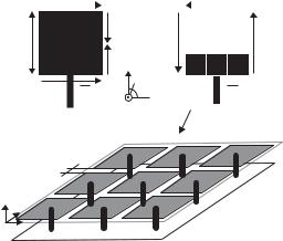
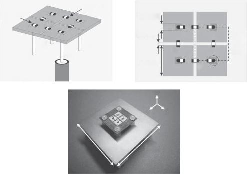
dimensions (λ0/10 × λ0/10 × λ0/10 over 0.45λ0 × 0.45λ0 ground plane; λ0: the operating wavelength). Figure 7.235 illustrates the antenna; (a) perspective view, (b) top view, and (c) 3D view. The NRI TL MM unit cell is constituted of a conventional TL, to which lumped capacitors and inductors are loaded to ensure series and shunt resonances respectively with parasitic inductance and capacitance inherently existing in the microstrip TL structure. By adjusting the values of the loaded elements and the unit cell size, amplitude and phase of signals propagating along an NRI TL structure can be aligned to obtain in-phase excitation of monopoles so that efficient radiation can be achieved. The monopoles are top-loaded with a square plate, on which the NRI TL MM structure is constituted, and consequently, appropriate radiation impedance to match 50 is attained even though the antenna height is very low. As can be seen in Figure 7.235(b), an NRI MM unit cell consists of a square plate, acting as a TL, to which a lumped inductance L0 is connected, and a lumped capacitance C0, bridging two TLs, thus resulting in an NRI TL MM.
Each of four square plates stands with a vertical post on a ground plane, one of which is the feeding post, and currents on each post are adjusted to be in-phase so that they are excited all in phase and efficient radiation can be obtained. It should be noted that use of folding monopole technology to increase the radiation resistance Rr, as was discussed in the previous section, is applied to this antenna structure, so obtained by placing an NRI MM between two posts.
242 |
Design and practice of small antennas I |
|
|
|
|
|
|
|
|
|
|
Wm |
|
|
|
|
|
|
|
|
|
Lm |
WC1 |
|
LR1 |
|
|
|
z |
||||||
|
|
|
|
|
|
||||||||||
|
|
|
|
|
|
|
|
|
y |
||||||
|
|
|
|
|
|
|
|
|
|
|
|
|
|
|
|
|
|
|
|
|
|
|
|
|
|
|
|
|
|
|
|
|
|
|
|
|
|
h |
|
|
|
|
|
FR4 |
x |
||
|
|
|
|
|
|
|
LR2 |
|
|
|
|||||
|
|
|
|
|
|
|
|||||||||
Ls2 |
|
|
|
|
Lg |
L1 |
|||||||||
Ls1 |
|
|
|
|
|
||||||||||
W |
Slot |
||||||||||||||
|
|
|
|
|
|
|
|
|
|
C2 |
|
|
|
C1 |
|
|
|
|
|
|
|
|
|
|
|
|
|
Ground |
|
||
|
|
|
|
|
|
|
|
|
|
|
|
||||
|
|
|
W |
|
|
|
|
Air |
|
|
L2 |
||||
|
|
|
|
S1 |
|
Wg2 |
|
|
C2 |
||||||
|
|
Wg1 |
|
|
bridge |
|
|
||||||||
|
|
|
|
|
|
|
|
|
|
|
|
|
|
||
|
|
|
|
|
|
|
|
|
|
|
|
|
SMA |
|
|
|
|
|
|
|
|
|
|
|
|
|
|
connector |
|
|
|
|
|
|
W |
g |
|
|
|
|
|
|
|
hsub |
|||
|
|
|
|
|
|
|
|
|
|
|
|
||||
|
|
|
|
|
|
|
|
|
|
||||||
|
|
|
|
|
|
(a) |
|
|
|
|
|
(b) |
|||
Figure 7.239 Tri-band monopole antenna with single-cell MTM loading and a defected-ground plane: (a) top view and (b) 3D view. ([123], copyright C 2010 IEEE).
Ground Structure (DGS) is defined as a unit cell EBG or an EBG with limited number of cells and a period.) The antenna geometry and the dimensional parameters are illustrated in Figure 7.239, where (a) is top view and (b) is 3D view. A coplanar waveguide (CPW)- fed monopole antenna is loaded with a single NRI TL MM-based Pi-unit cell. The series capacitance C1 is formed between the monopole on the top of the substrate and the rectangular patch placed opposite to the monopole. The TL MM cell is asymmetrically loaded with two shunt inductances, L1 and L2. As can be seen in Figure 7.239, L1 is formed by the inductive strip to feed the monopole and L2 is formed by the thin inductive strip that connects the rectangular patch beneath the monopole to the rectangular patch beneath the RH ground plane (GP). A capacitance C2, formed between the rectangular patch and the RH GP, connects the shunt inductor L2 to the ground. By appropriately adjusting these parameters in addition to the geometrical parameters of the antenna, current flows on the feed strip (L1) to the monopole and the inductive strip (L2) to the rectangular patch behind the monopole, can be made in-phase at the resonance frequency, thus the antenna performs effectively as a two-arm folded monopole. Figure 7.240(a) shows the current flows with arrows and indicates the antenna operates in the folded monopole mode. The resonance frequency in this case is around 5.0 GHz–6.0 GHz.
In this antenna structure loaded with an NRI TL MM, resonance occurs at lower frequency around 2.4 GHz–2.5 GHz in addition to the higher frequency with other modes. Major current flows on the GP are depicted in Figure 7.240(b), which shows that the currents along the CPW feed line are symmetric, while those on the upper edges of the GP are in-phase. This means that the currents on the edges of the GP contribute radiation and the antenna effectively performs as a dipole, which radiates in a direction orthogonal to that of the monopole mode. The in-phase currents on the top edges of the GP are produced by designing the series circuit comprising C1, C2, L1 and L2 to resonate at a frequency that overlaps with the dipole mode resonance, as the series circuit becomes short. The resonance frequency depends on the length of the current path, related with the size of the GP, Wg + 2Lg, (Figure 7.239). Based on the design consideration discussed above, the optimized loading patches have dimensions
7.2 Design and practice of ESA |
243 |
|
|
z |
y |
|
|
|
|
|
z |
|
y |
||
|
|
|
|
||
|
|
|
|
|
|
x |
x |
|
|
|
|
(a) |
|
(b) |
|
|
|
|
|
|
z y
x
(c)
Figure 7.240 Current distributions on the conductor of the tri-band monopole antenna shown in Figure 7.239: (a) folded monopole mode (5.80 GHz), (b) dipole mode (2.44 GHz), and (c) effect of defected ground plane (3.76 GHz) ([123], copyright C 2010 IEEE).
of 3.0 mm × 3.0 mm and 2.5 mm × 2.5 mm, respectively, and the two sections of thin strips have the same length of 5.5 mm and width of 0.25 mm. As the current flow takes a longer path than the length of the edge of the GP, a lower resonance frequency is achieved in comparison with the antenna introduced in the previous section [122], where the dipole-mode currents flow only on the top edges of the GP. This implies that a larger miniaturization factor is attained by this antenna structure.
In addition to the dipole mode, the antenna is designed to perform with a third mode, which is achieved by using a defected GP structure, formed by cutting an L-shaped slot out on the left-side of the CPW on the GP as shown in Figure 7.240. With this slot, resonance occurs around 3.5 GHz, while the dual-mode operation at around 2.5 GHz and 6.0 GHz is preserved. Current distributions on the GP at the resonance frequency


 Simulated
7.2 Design and practice of ESA |
245 |
|
|
Dielectric Ground plane
Vias
Coax feed |
Metal patches Gaps |
y |
 x
x
z
g1

 d Wm w
 Lm
Lm 
 g2
g2
L
|
Metal patches |
h |
Dielectric |
|
Ground plane |
Coax probe |
Vias |
Figure 7.242 Microstrip patch antenna partially filled with a 2 × 1 arrangement of CRLH cells ([124], copyright C 2008 IEEE).
adjacent cells is obtained, giving lower operating frequency and leading to miniaturization of the antenna.
Meanwhile, the square patch is a conventional microstrip antenna, which is modeled as an open-ended TL resonator, composed equivalently with a series inductance Lms and a shunt capacitance Cms. The propagation constant βRH along this RH TL structure is expressed by
βRH = ω Lms Cms . (7.79)
The square patch partially loaded with a CRLH structure is treated as a combined TL of two RH and one LH TL structures. An open ended or short circuited RH + LH + RH TL works as a resonator that exhibits a behavior similar to a CRLH resonator at lower

246Design and practice of small antennas I
frequencies and a RH resonator at higher frequencies. The propagation constant along the LH section is given by
βLH = −1/( pω L L CL ) (7.80)
where p denotes the length of the unit cell, smaller than λg/4 and LL and CL, respectively, are inductance and capacitance per unit cell. The antenna is designed to operate at three modes, n = ± 1 and 0.
At lower frequencies, where |βLH| > |βRH|, an antenna with a mode n = –1 can be obtained as β–1 L = – π (β–1: the propagation constant along the TL of the length L at n = –1, and L: the length of the RH + LH + RH TL structure). The antenna operates here with a fundamental mode just as a conventional patch, which has two radiating slots having the same amplitude and opposite phase, thus the radiation pattern is dipolar.
As the frequency increases, βLH increases, while βRH decreases. Then, a mode n = 0 can be excited by making βLH + βRH = β0 L = 0. The electric field distribution of this mode is constant, and so two radiation slots of the patch have the same amplitude and phase, leading to a monopole-like radiation at the resonance frequency f0.
At frequencies higher than f0, |βLH| is greater than |βRH| and thus the resonance condition for n = +1 mode can be achieved, where β+1 L = + π . This mode has the same field distribution and radiation property as the fundamental mode of the conventional patches.
Since the frequencies of the lower modes n ≤ 0 depend on the CRLH (mushroom) structure, desired operating frequencies at lower bands are obtained by appropriate design of the mushroom structure.
For desired operating frequencies at higher bands, as the frequencies at higher mode n = +1 depend on the patch itself, the patch dimensions are so designed as the conventional patch without mushroom.
The proposed antenna having dimensions of (L × W) = 42 mm × 42 mm, the substrate with εr = 2.2 and thickness h = 10 mm is used. The mushroom structure is comprised with a 2 × 1 cell array and has the dimensions (Lm × Wm) 10.6 mm × 17.8 mm, the gap between the two mushrooms is 0.40 mm, and the separation gap between the LH structure and the microstrip patch is 0.2 mm. The diameter of the vias is 0.7 mm. The coaxial feed probe is placed 14 mm from the center and the size of the GP is 80 mm × 80 mm. These dimensional parameters are chosen to obtain the resonant frequencies at 1 GHz for the n = –1 mode, used in GSM (Global Systems for Mobile Communications), at 1.5 GHz for the n = 0 mode, used in navigation systems, and 2.2 GHz for n = +1 mode, used in UMTS (Universal Mobile Telephone Systems).
Experimental results are: for n = –1 mode (f0 = 1.06 GHz), D (directivity) = 4.5 dB, G (Gain) = –3 dB, E (efficiency) = 17.8%, and BW (–6 dB bandwidth) = 3%; for the n = 0 mode (f0 = 1.45 GHz), D = 5.1 dB, G = 1 dB, E = 39%, BW = 3%; and for the n = +1 mode (f0 = 2.16 GHz), D = 7.4 dB, G = 6.5 dB, E = 82%, and BW = 13%. The lengths of the antenna in terms of the resonance frequency are λ0/6.74, λ0/4.92, and λ0/3.31 for the mode n = –1, 0, and +1, respectively, indicating that at the lower modes, significant reduction of the antenna size is observed compared with the conventional λ/2 patch antenna. The antenna presents two dipole modes (n = ±1) and one monopole
7.2 Design and practice of ESA |
247 |
|
|
Antenna
 y
y
 x
x
|
|
|
|
Feeding |
|
|
|
|
|
||
Ground |
|||||
line |
|||||
plane |
|||||
|
|||||
|
|
|
|
|
|
Figure 7.243 Geometry of the RH/LH TLs loaded planar antenna ([125], copyright C 2008 IEEE).
mode (n = 0), and radiation patterns at the different operating modes are dipolar and monopolar.
A dual-frequency patch antenna, which aims at application to DCS at 1.8 GHz and UMTS at 2.2 GHz, was designed by using the same concept and an example is shown in [124]. In this case, a 2 × 2 CRLH structure is employed so that the two modes are excited, excluding n = 0 mode. The mushroom configuration was changed to be square and the number of cells was increased to four. The dimensions of this antenna are larger than the first one, with length of λ0/3.44 at the lower frequency and λ0/2.83 at the higher frequency. With increased size, efficiency of the antenna is made higher (60%) than the first one for n = –1.
7.2.5.2.3.6 Compact CRLH MM-loaded slot antenna
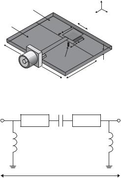
A planar antenna utilizing cascaded RH/LH TLs to realize compact size is introduced in [125]. The antenna geometry is depicted in Figure 7.243, where the constitutive elements of the RH/LH TL are shown by black parts (printed capacitors) and slots (inductors). The RH TL consists of a series inductance and a shunt capacitance in a Pi-network structure, while the LH TL consists of a series capacitance and a shunt inductance in a T-network structure. They are connected with an open-circuit at the unconnected port of the LH TL, by which the TL works as a resonator. Along the power travelling direction, the RH and LH TLs have opposite phase property from each other, hence a ZOR (zeroth-order resonance) structure can be formed and the size of the antenna can be designed arbitrarily without regard to the wavelength since it is specified by the circuit parameters. The circuit elements are realized by using printed elements. The size of printed patches is designed to have proper capacitance against the ground, while the length of the metal traces or the size of slots on the ground plane is designed to create required inductance. The realized proposed antenna of straight type is shown in Figure 7.244. Layout of the antenna of L-shaped type is illustrated in Figure 7.245(a), in which dark lines show the top metal part and dotted lines give the bottom metal part. In the figure, (a) shows that three patches on the top metal part realize capacitances C1, C2, and C3, respectively, and two narrow metal slots placed on the bottom metal, which
248 |
Design and practice of small antennas I |
|
|
|
|
|
|
C3 |
|
|
|
|
|
|
|
|
|
|
|
|
|
|
|
|
|
|
|
|
|
|
|
|
|
|
|
|
|
|
|
|
|
|
|
|
|
|
||||
|
|
|
|
|
|
|
|
|
|
L2 |
|
|
|
|
|
|
|
|
|
|
|
|
|
|
|
|
|
|
|
|
|
|
|
|
|
|
|
|
|
|
|
|
|
|||
|
|
|
|
C2 |
|
|
|
|
|
|
|
|
|
|
|
|
|
|
|
|
|
|
|
y |
|
|
|
|
|
|
|
|
||||||||||||||
y |
|
|
|
|
|
|
|
|
|
|
|
|
|
|
|
|
|
|
|
|
|
|
|
|
|
|
|
|
|
|
|
x |
|
|
|
|
|
|
|
|
||||||
|
|
|
|
|
|
|
|
|
|
|
|
|
|
|
|
|
|
|
|
|
|
|
|
|
|
|
|
|
|
|
|
|
|
|
|
|
|
|
||||||||
|
|
|
|
L1 |
|
|
|
|
|
|
|
|
|
|
|
|
|
|
|
|
|
|
|
|
|
|
|
|
|
|
|
|
|
|
|
|
||||||||||
|
|
|
|
|
|
|
|
|
|
|
|
|
|
|
|
|
|
|
|
|
|
|
|
|
|
|
|
|
|
|
|
|
|
|
|
|
||||||||||
|
x |
|
|
|
|
|
|
|
|
|
|
|
|
|
|
|
|
|
|
|
|
|
|
|
|
|
|
|
|
|
|
|
|
|
|
|
|
|
|
|
|
|
|
|
|
|
|
|
|
C1 |
|
|
|
|
|
|
|
|
|
|
|
|
|
|
|
|
|
|
|
|
|
|
|
|
|
C1 |
|
L1 |
|
C2 |
|
C3 |
|
||||||||||
|
|
|
|
|
|
|
|
|
|
|
|
|
|
|
|
|
|
|
|
|
|
|
|
|
|
|
|
|
|
|
|
|
|
|||||||||||||
|
|
|
|
|
|
|
|
|
|
|
|
|
|
|
|
|
|
|
|
|
|
|
|
|
|
|
|
|
|
|
|
|
|
|
|
|
|
|
||||||||
|
|
|
|
|
|
|
|
|
|
|
|
|
|
|
|
|
|
|
|
|
|
|
|
|
|
|
|
|
|
|
|
|
|
|
|
|
|
|
|
|
|
|
|
|
|
|
|
|
|
|
|
|
|
|
|
|
|
|
|
|
|
|
|
|
|
|
|
|
|
|
|
|
|
|
|
|
|
|
|
|
|
|
|
|
|
|
|
|
|
|
|
L2 |
|
|
|
|
|
|
|
|
|
|
|
|
|
|
|
|
|
|
|
|
|
|
|
|
|
|
|
|
|
|
|
|
|
|
|
|
|
|
|
|
|
|
|
|
|
|
|
|
|
|
|
|
|
|
|
|
|
|
|
|
|
|
|
|
|
|
|
|
|
|
|
|
|
|
|
|
|
|
|
|
|
|
|
|
|
|
|
|
|
|
|
|
|
|
|
|
|
|
|
|
(a) |
|
|
|
|
|
|
|
|
|
|
|
|
|
|
|
|
|
|
|
|
|
|
|
|
|
|
|
|
(b) |
|
|
|
|||||||||
|
Figure 7.244 Layout of straight type antenna, (a) horizontal arrangement and (b) vertical |
|||||||||||||||||||||||||||||||||||||||||||||
|
arrangement ([125], copyright C 2005 IEEE). |
|
|
|
|
|
|
|
|
|||||||||||||||||||||||||||||||||||||
|
|
|
|
|
|
|
|
|
|
|
|
|
|
|
|
|
|
|
|
W |
|
|
|
|
|
|
|
|
|
|
|
|
|
|
|
|
|
|
|
|
|
|
||||
|
|
|
|
|
|
|
|
|
|
|
|
|
|
|
|
|
|
|
|
|
|
|
|
|
Ls1 |
|
|
|
|
|
|
|
|
|
|
|
|
|
|
|
|
L1 |
|
C3 |
||
|
|
|
|
|
|
|
|
|
|
|
|
|
|
|
|
|
|
|
|
|
|
|
|
|
|
|
|
|
|
|
|
|
|
|
|
|
|
|
|
|
|
|
|
|
||
|
|
|
|
|
|
|
|
|
|
|
|
|
|
|
|
|
|
|
|
|
|
|
|
|
|
|
|
|
|
|
|
|
|
|
|
|
|
|
|
|
|
|
|
|
||
|
|
|
|
|
|
|
|
|
|
|
|
|
|
|
|
|
|
|
|
|
|
|
|
|
|
|
|
|
|
|
|
|
|
|
|
|
|
|
|
|
|
|
|
|
||
|
|
|
|
|
|
|
|
|
|
|
|
|
|
|
|
|
|
|
|
|
|
|
|
|
C3 |
|
|
|
|
|
|
|
|
|
|
|
|
|
|
|
|
|
||||
|
|
|
|
|
|
|
|
|
|
|
|
|
|
|
|
|
|
|
|
|
|
|
|
|
|
|
|
|
|
|
|
|
|
|
|
|
|
|
|
|
|
|
||||
|
|
|
|
|
|
|
|
|
|
|
|
L2 |
|
|
|
|
|
|
|
|
|
|
|
|
|
|
|
|
|
|
|
|
|
|
||||||||||||
|
(a) L |
|
|
|
|
|
|
|
|
|
|
|
|
|
|
|
|
|
|
|
|
|
|
|
|
|
|
|
|
|
|
|
|
|
|
|||||||||||
|
|
|
|
|
|
|
|
|
|
|
|
|
|
|
|
|
|
|
|
|
|
|
|
|
|
|
|
|
|
|
|
|
|
|
L |
|
|
|
|
|
|
|
L2 |
|||
|
|
|
|
|
|
|
|
|
|
|
|
|
|
|
|
|
|
|
|
|
|
|
|
|
|
|
|
|
|
|
|
|
|
|
|
|
|
s3 |
|
|
|
|
|
|
||
|
|
|
|
|
|
|
|
|
|
|
|
|
|
|
|
|
|
|
|
|
|
|
L |
1 |
|
|
|
|
|
|
|
Ls2 |
|
|
|
|
(b) |
|
|
|
C1 |
C2 |
||||
|
|
|
|
|
|
|
|
|
|
|
|
|
|
|
|
|
|
|
|
|
|
|
|
|
|
|
|
|
|
|
|
|
|
|
|
|
|
|
|
|
|
|
||||
|
|
|
|
w |
|
|
|
|
|
C1 |
|
|
|
|
|
|
C2 |
|
|
|
|
|
|
|
|
|
|
Zin |
|
|
|
|||||||||||||||
|
|
|
|
|
|
|
|
|
|
|
|
|
|
|
|
|
|
|
|
|
|
|
|
|
|
|
|
|
|
|
||||||||||||||||
|
|
|
|
|
|
|
|
|
|
|
|
|
|
|
|
|
|
|
|
|
|
|
|
|
|
|
|
|
||||||||||||||||||
|
|
|
|
|
c |
|
|
|
|
|
|
|
|
|
|
|
|
|
|
|
|
|
|
|
|
|
|
|
|
|
|
|
|
|
|
|
|
|
|
|
|
|
|
|
|
|
|
|
|
|
|
|
|
|
|
|
|
|
|
|
|
|
|
|
|
|
|
|
|
|
|
|
|
|
|
|
|
|
|
|
|
|
|
|
|
|
|
|
|
|
|
|
|
|
|
|
|
|
|
|
|
|
|
wc |
|
|
|
|
|
g |
wc |
|
|
|
|
|
|
|
|
|
|
|
|
|
|
|
|
|
|
|
|
|||||||||
|
|
|
|
|
|
|
|
|
|
|
|
|
|
|
|
|
|
|
|
|
|
|
|
|
|
|
|
|
|
|
|
|
|
|
|
|
|
|
|
|
|
|
|
|
|
|
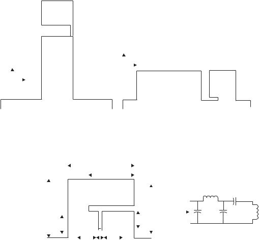
Figure 7.245 Layout of L-shaped type (a) the composition of metamaterial components and (b) the equivalent circuit of a π -model for RH TL and a T-model for LH TL ([125], copyright C 2008 IEEE).
is considered as the ground plane (GP), produce inductances L1 and L2. A closed loop is formed by these elements, on which current flows in order of C1, L1, C2, C3, and L2, and then back to C1. The dimensional parameters (in mm) are L = W = 11.5, wc = 4, Ls3 = 9.5, g = 1.3, Ls1 = 7.2, Ls2 = 3.2, and the slot (L1) width is 0.5. The size of the GP is 40 mm × 30 mm. All three capacitances are designed to have the same value 2.6 pF and both inductances have the same value of 1.62 nH. The equivalent circuit consisting of these circuit elements is given in Figure 7.245(b). Magnetic currents flow around C2 and C3, but currents on both sides have opposite phase and do not contribute to radiation, while the top sides of both elements operate as the radiating edges, and contribute to radiation. Since the field produced by C1 is very weak, it is not taken into