

- •Contents
- •Preface
- •Chapter 1 Introduction (K. Fujimoto)
- •Chapter 2 Small antennas (K. Fujimoto)
- •Chapter 3 Properties of small antennas (K. Fujimoto and Y. Kim)
- •Chapter 4 Fundamental limitation of small antennas (K. Fujimoto)
- •Chapter 5 Subjects related with small antennas (K. Fujimoto)
- •Chapter 6 Principles and techniques for making antennas small (H. Morishita and K. Fujimoto)
- •Chapter 7 Design and practice of small antennas I (K. Fujimoto)
- •Chapter 8 Design and practice of small antennas II (K. Fujimoto)
- •Chapter 9 Evaluation of small antenna performance (H. Morishita)
- •Chapter 10 Electromagnetic simulation (H. Morishita and Y. Kim)
- •Chapter 11 Glossary (K. Fujimoto and N. T. Hung)
- •Acknowledgements
- •1 Introduction
- •2 Small antennas
- •3 Properties of small antennas
- •3.1 Performance of small antennas
- •3.1.1 Input impedance
- •3.1.4 Gain
- •3.2 Importance of impedance matching in small antennas
- •3.3 Problems of environmental effect in small antennas
- •4 Fundamental limitations of small antennas
- •4.1 Fundamental limitations
- •4.2 Brief review of some typical work on small antennas
- •5 Subjects related with small antennas
- •5.1 Major subjects and topics
- •5.1.1 Investigation of fundamentals of small antennas
- •5.1.2 Realization of small antennas
- •5.2 Practical design problems
- •5.3 General topics
- •6 Principles and techniques for making antennas small
- •6.1 Principles for making antennas small
- •6.2 Techniques and methods for producing ESA
- •6.2.1 Lowering the antenna resonance frequency
- •6.2.1.1 SW structure
- •6.2.1.1.1 Periodic structures
- •6.2.1.1.3 Material loading on an antenna structure
- •6.2.2 Full use of volume/space circumscribing antenna
- •6.2.3 Arrangement of current distributions uniformly
- •6.2.4 Increase of radiation modes
- •6.2.4.2 Use of conjugate structure
- •6.2.4.3 Compose with different types of antennas
- •6.2.5 Applications of metamaterials to make antennas small
- •6.2.5.1 Application of SNG to small antennas
- •6.2.5.1.1 Matching in space
- •6.2.5.1.2 Matching at the load terminals
- •6.2.5.2 DNG applications
- •6.3 Techniques and methods to produce FSA
- •6.3.1 FSA composed by integration of components
- •6.3.2 FSA composed by integration of functions
- •6.3.3 FSA of composite structure
- •6.4 Techniques and methods for producing PCSA
- •6.4.2 PCSA employing a high impedance surface
- •6.5 Techniques and methods for making PSA
- •6.5.2 Simple PSA
- •6.6 Optimization techniques
- •6.6.1 Genetic algorithm
- •6.6.2 Particle swarm optimization
- •6.6.3 Topology optimization
- •6.6.4 Volumetric material optimization
- •6.6.5 Practice of optimization
- •6.6.5.1 Outline of particle swarm optimization
- •6.6.5.2 PSO application method and result
- •7 Design and practice of small antennas I
- •7.1 Design and practice
- •7.2 Design and practice of ESA
- •7.2.1 Lowering the resonance frequency
- •7.2.1.1 Use of slow wave structure
- •7.2.1.1.1 Periodic structure
- •7.2.1.1.1.1 Meander line antennas (MLA)
- •7.2.1.1.1.1.1 Dipole-type meander line antenna
- •7.2.1.1.1.1.2 Monopole-type meander line antenna
- •7.2.1.1.1.1.3 Folded-type meander line antenna
- •7.2.1.1.1.1.4 Meander line antenna mounted on a rectangular conducting box
- •7.2.1.1.1.1.5 Small meander line antennas of less than 0.1 wavelength [13]
- •7.2.1.1.1.1.6 MLAs of length L = 0.05 λ [13, 14]
- •7.2.1.1.1.2 Zigzag antennas
- •7.2.1.1.1.3 Normal mode helical antennas (NMHA)
- •7.2.1.1.1.4 Discussions on small NMHA and meander line antennas pertaining to the antenna performances
- •7.2.1.2 Extension of current path
- •7.2.2 Full use of volume/space
- •7.2.2.1.1 Meander line
- •7.2.2.1.4 Spiral antennas
- •7.2.2.1.4.1 Equiangular spiral antenna
- •7.2.2.1.4.2 Archimedean spiral antenna
- •7.2.2.1.4.3.2 Gain
- •7.2.2.1.4.4 Radiation patterns
- •7.2.2.1.4.5 Unidirectional pattern
- •7.2.2.1.4.6 Miniaturization of spiral antenna
- •7.2.2.1.4.6.1 Slot spiral antenna
- •7.2.2.1.4.6.2 Spiral antenna loaded with capacitance
- •7.2.2.1.4.6.3 Archimedean spiral antennas
- •7.2.2.1.4.6.4 Spiral antenna loaded with inductance
- •7.2.2.2 Three-dimensional (3D) structure
- •7.2.2.2.1 Koch trees
- •7.2.2.2.2 3D spiral antenna
- •7.2.2.2.3 Spherical helix
- •7.2.2.2.3.1 Folded semi-spherical monopole antennas
- •7.2.2.2.3.2 Spherical dipole antenna
- •7.2.2.2.3.3 Spherical wire antenna
- •7.2.2.2.3.4 Spherical magnetic (TE mode) dipoles
- •7.2.2.2.3.5 Hemispherical helical antenna
- •7.2.3 Uniform current distribution
- •7.2.3.1 Loading techniques
- •7.2.3.1.1 Monopole with top loading
- •7.2.3.1.2 Cross-T-wire top-loaded monopole with four open sleeves
- •7.2.3.1.3 Slot loaded with spiral
- •7.2.4 Increase of excitation mode
- •7.2.4.1.1 L-shaped quasi-self-complementary antenna
- •7.2.4.1.2 H-shaped quasi-self-complementary antenna
- •7.2.4.1.3 A half-circular disk quasi-self-complementary antenna
- •7.2.4.1.4 Sinuous spiral antenna
- •7.2.4.2 Conjugate structure
- •7.2.4.2.1 Electrically small complementary paired antenna
- •7.2.4.2.2 A combined electric-magnetic type antenna
- •7.2.4.3 Composite structure
- •7.2.4.3.1 Slot-monopole hybrid antenna
- •7.2.4.3.2 Spiral-slots loaded with inductive element
- •7.2.5 Applications of metamaterials
- •7.2.5.1 Applications of SNG (Single Negative) materials
- •7.2.5.1.1.2 Elliptical patch antenna
- •7.2.5.1.1.3 Small loop loaded with CLL
- •7.2.5.1.2 Epsilon-Negative Metamaterials (ENG MM)
- •7.2.5.2 Applications of DNG (Double Negative Materials)
- •7.2.5.2.1 Leaky wave antenna [116]
- •7.2.5.2.3 NRI (Negative Refractive Index) TL MM antennas
- •7.2.6 Active circuit applications to impedance matching
- •7.2.6.1 Antenna matching in transmitter/receiver
- •7.2.6.2 Monopole antenna
- •7.2.6.3 Loop and planar antenna
- •7.2.6.4 Microstrip antenna
- •8 Design and practice of small antennas II
- •8.1 FSA (Functionally Small Antennas)
- •8.1.1 Introduction
- •8.1.2 Integration technique
- •8.1.2.1 Enhancement/improvement of antenna performances
- •8.1.2.1.1 Bandwidth enhancement and multiband operation
- •8.1.2.1.1.1.1 E-shaped microstrip antenna
- •8.1.2.1.1.1.2 -shaped microstrip antenna
- •8.1.2.1.1.1.3 H-shaped microstrip antenna
- •8.1.2.1.1.1.4 S-shaped-slot patch antenna
- •8.1.2.1.1.2.1 Microstrip slot antennas
- •8.1.2.1.1.2.2.2 Rectangular patch with square slot
- •8.1.2.1.2.1.1 A printed λ/8 PIFA operating at penta-band
- •8.1.2.1.2.1.2 Bent-monopole penta-band antenna
- •8.1.2.1.2.1.3 Loop antenna with a U-shaped tuning element for hepta-band operation
- •8.1.2.1.2.1.4 Planar printed strip monopole for eight-band operation
- •8.1.2.1.2.2.2 Folded loop antenna
- •8.1.2.1.2.3.2 Monopole UWB antennas
- •8.1.2.1.2.3.2.1 Binomial-curved patch antenna
- •8.1.2.1.2.3.2.2 Spline-shaped antenna
- •8.1.2.1.2.3.3 UWB antennas with slot/slit embedded on the patch surface
- •8.1.2.1.2.3.3.1 A beveled square monopole patch with U-slot
- •8.1.2.1.2.3.3.2 Circular/Elliptical slot UWB antennas
- •8.1.2.1.2.3.3.3 A rectangular monopole patch with a notch and a strip
- •8.1.2.1.2.3.4.1 Pentagon-shape microstrip slot antenna
- •8.1.2.1.2.3.4.2 Sectorial loop antenna (SLA)
- •8.1.3 Integration of functions into antenna
- •8.2 Design and practice of PCSA (Physically Constrained Small Antennas)
- •8.2.2 Application of HIS (High Impedance Surface)
- •8.2.3 Applications of EBG (Electromagnetic Band Gap)
- •8.2.3.1 Miniaturization
- •8.2.3.2 Enhancement of gain
- •8.2.3.3 Enhancement of bandwidth
- •8.2.3.4 Reduction of mutual coupling
- •8.2.4 Application of DGS (Defected Ground Surface)
- •8.2.4.2 Multiband circular disk monopole patch antenna
- •8.2.5 Application of DBE (Degenerated Band Edge) structure
- •8.3 Design and practice of PSA (Physically Small Antennas)
- •8.3.1 Small antennas for radio watch/clock systems
- •8.3.2 Small antennas for RFID
- •8.3.2.1 Dipole and monopole types
- •8.3.2.3 Slot type antennas
- •8.3.2.4 Loop antenna
- •Appendix I
- •Appendix II
- •References
- •9 Evaluation of small antenna performance
- •9.1 General
- •9.2 Practical method of measurement
- •9.2.1 Measurement by using a coaxial cable
- •9.2.2 Method of measurement by using small oscillator
- •9.2.3 Method of measurement by using optical system
- •9.3 Practice of measurement
- •9.3.1 Input impedance and bandwidth
- •9.3.2 Radiation patterns and gain
- •10 Electromagnetic simulation
- •10.1 Concept of electromagnetic simulation
- •10.2 Typical electromagnetic simulators for small antennas
- •10.3 Example (balanced antennas for mobile handsets)
- •10.3.2 Antenna structure
- •10.3.3 Analytical results
- •10.3.4 Simulation for characteristics of a folded loop antenna in the vicinity of human head and hand
- •10.3.4.1 Structure of human head and hand
- •10.3.4.2 Analytical results
- •11 Glossary
- •11.1 Catalog of small antennas
- •11.2 List of small antennas
- •Index
7.2 Design and practice of ESA |
253 |
|
|
4396B 1.8 μH 33 pF
(a) |
50 |
1Ω |
|
≈ 4Ω
1.8 μH 33 pF
(b) 4396B |
1.8 μH 33 pF |
neg L, C |
|
50 |
1Ω |
≈ 4Ω
Figure 7.251 Matching circuits for small antenna: (a) passive case and (b) active case [132].
The active matching showed power efficiency that exceeds 20 dB over that of the passive matching for the lower frequency band. The class B biasing demonstrates higher peak power delivery (about 24 dBm) than the best possible passive match near the center frequency (23 MHz) of the band, while the class A biasing shows nearly constant power level (15 dBm over the passive case) for the entire frequency band (15–30 MHz).
Application of NIC circuits to a receiver is discussed in [133]. A six-inch monopole antenna is used and the transmitter used for evaluation of the receiver performance is arranged to transmit the frequency of 20–110 MHz. The receiver has 4 dB noise figure achieved by using a low noise RF amplifier. In the matching circuit an NIC is used to represent –Ca as shown in Figure 7.246. At 30 MHz, the antenna reactance –730 was brought down to –14.6 , not zero reactance, after the NIC. This results from the inevitable parasitic reactance. Measured signal-to-noise ratio (S/N) exhibits improvement of 6 to a few dB over the entire frequency band. Figure 7.252 gives comparison of S1/N1 (active matching case) to S0/N0 (a case when the antenna and the receiver are directly connected).
7.2.6.2Monopole antenna
Active circuit matching is described in [134], in which a case where an electrically small monopole placed on the infinite ground plane is considered. A two-port circuit model representing an antenna system is considered through simulation and the antenna performances, radiation efficiency, and bandwidth, of both passive and active matching cases are studied. The antenna considered here is a cylindrical monopole of 0.6 m in length and 0.010 m in diameter and the operating frequency is assumed to be 30 to 90 MHz. The matching circuit is basically the same as that shown in Figure 7.250, where an NIC is used to implement negative reactance corresponding to the series

254 |
Design and practice of small antennas I |
|
|
dB
70 10log (S1/N1)  60
60
50
40 |
|
30 |
10log (S0/N0) |
20
20 30 40 50 60 70 80 90 100 110
Frequency (MHz)
Figure 7.252 Comparison of S/N between passive and active matching cases [133].
antenna capacitance Ca and inductance La and an inductance Lm of the transformer
section that converts the small antenna resistance to 50 (the load resistance). Lm
√
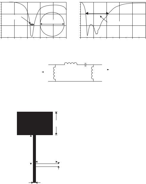
here is designed to equal R0 Z0/ω0 where Z0 is the desired impedance level, which is here 50 . The active device used is a silicon bipolar NPN transistor. Simulated return loss and total efficiency of the antenna/matching network combination are illustrated in Figure 7.253, where (a) is the passive matching case and (b) is the active matching case. As can be seen in the figure, the bandwidth is extended from about 3 MHz (–3 dB efficiency) in the passive case to about 36 MHz to beyond 90 MHz (–10 dB return loss) in the active case. The total efficiency in the active case is better than 95% from about 36 MHz to above 90 MHz.
Another example of NIC application to a small monopole antenna is introduced in [135]. The antenna is a 3-inch wire monopole with 1.5 mm diameter placed on a finite ground plane (3 inch × 3 inch with 1 mm thickness) and a negative capacitor to make a 50 load (generator) match to the antenna, for which an NIC is used. The frequency range considered is 1 MHz to 1 GHz. The total reactance of the antenna in the active matching case becomes lower than that of the antenna in the passive matching case. Consequently the transducer gain between the source and the antenna becomes 16.23 dB higher in the frequency range from 50 MHz to 644 MHz in the active matching case. This result is significant, since the antenna electrical length is very small; λ/79 at 50 MHz and λ/6 at 644 MHz.
7.2.6.3Loop and planar antenna
To improve the bandwidth and reduce the size of the antenna, a non-Foster matching network is designed. A loop antenna is considered as an example. As a small loop antenna has different impedance behavior from that of a small dipole, the matching circuit must be optimized to meet the variation of the loop impedance. Then the circuit consisting of a shunt inductance and an optimized non-Foster network is taken into consideration [136]. Return loss of a 6-inch loop is depicted in Figure 7.254(a), where the inset shows the loop, and the return loss of the antenna with active matching network

7.2 Design and practice of ESA |
255 |
|
|
(a)0
(dB)loss −10 Return
−20
30 40
|
|
|
|
100 |
|
|
Return loss |
|
|
|
|
|
|
(%) |
|
|
|
|
Totalefficiency |
|
|
|
|
50 |
|
|
|
Total efficiency |
|
|
|
|
|
0 |
50 |
60 |
70 |
80 |
90 |
Frequency (MHz)
(b)0
|
−10 |
Total efficiency |
|
|
|
|
|
|
|
|
|
(dB) |
|
|
|
Return loss |
|
−20 |
|
|
|
|
|
loss |
|
|
|
|
|
|
|
|
|
|
|
Return |
−30 |
|
|
|
|
|
|
|
|
|
|
|
−40 |
|
|
|
|
|
−50 |
|
|
|
|
|
30 |
40 |
50 |
60 |
70 |
Frequency (MHz)
110 |
|
|
100 |
|
|
|
(%) |
|
90 |
efficiency |
|
|
||
80 |
Total |
|
70 |
||
|
||
60 |
|
80 90
Figure 7.253 Return losses: (a) passive matching case and (b) active matching case ([134], copyright C 2008 IEEE).
is given in Figure 7.254(b). The optimized non-Foster matching network is shown in Figure 7.254(c). From (a) and (b), increased bandwidth from 50 MHz to over 320 MHz can be observed after the non-Foster matching network is used.
In [136], a planar dipole antenna, to which a non-Foster matching network is applied, is treated. The antenna is printed on a very thin, flexible dielectric sheet, and the antenna size is λ/4 × λ/5 at 250 MHz. It has a gain greater than 0 dB from 250 MHz to 1000 MHz, meaning 4 to 1 bandwidth. Since a simple matching circuit at the feed is not sufficient, two additional ports apart from the feed point within the antenna structure are defined, to which negative capacitances are added, producing a resistance around 50 from 50 MHz to 300 MHz. With this resistance the optimized matching circuit is designed by using a non-Foster matching network, in which three negative inductances
256 |
Design and practice of small antennas I |
|
|
0 |
|
|
|
|
|
0 |
|
|
|
|
|
−5 |
50 MHz |
|
|
|
−10 |
|
|
|
|
|
|
|
|
|
|
|
|
|
|
|
|
|
|
|
|
|
|
6” (inch) |
|
|
320 MHz |
|
|
||
−10 |
|
|
|
|
−20 |
|
|
|
|||
|
|
|
|
|
|
|
|
|
|||
−15 |
|
|
|
|
−30 |
|
|
|
|
|
|
0.2 |
0.4 |
0.6 |
0.8 |
1.0 |
1.2 |
0.2 |
0.4 |
0.6 |
0.8 |
1.0 |
1.2 |
|
|
|
GHz |
|
|
|
|
|
GHz |
|
|
|
|
|
(a) |
|
|
|
|
|
(b) |
|
|
|
|
|
|
|
−112 nH |
−0.5 pF |
|
|
|
|
|
|
|
|
|
Feed |
|
|
|
Antenna |
|
|
|
|
|
|
(c) |
28 nH |
|
−500 nH |
|
|
|
||
|
|
|
|
|
|
|
|
||||
Figure 7.254 Matching performance of a 6-inch loop: return loss in the case of (a) passive matching, (b) active matching, and (c) Non-Foster matching network ([136], copyright C 2009 IEEE).
 W = 16 mm

L = 9 mm
L1 |
= 17 mm |
Lstub = 10.07 mm |
||||
|
|
|||||
|
|
|
|
|
|
|
|
|
|
|
|
|
|

 W2 = 1.19 mm
W1 = 2.31 mm
Figure 7.255 The reference antenna ([137], copyright C 2007 IEEE).
and two negative capacitances are used. As a consequence, the imaginary part of the antenna impedance is cancelled from around 80 MHz to 275 MHz. This results in size reduction of the antenna having a λ/12 × λ/18 planar dipole with a 3.5 to 1 bandwidth (80 MHz to 270 MHz) with gain greater than 0 dBi.