

7.2 Design and practice of ESA |
143 |
|
|
Table 7.7 Parameters of basic meander lines of three types; N1, N2, and N3, shown in Figure 7.85 [35]
Antennas |
f0(MHz) |
Rrad( ) |
Q |
kr |
N1 |
543.44 |
26.52 |
59.8 |
0.499 |
N2 |
548 |
120 |
59 |
0.498 |
N3 |
325.1 |
5.362 |
74.6 |
0.296 |
|
|
|
|
|
N1 |
N2 |
N3 |
Figure 7.85 Variation of meander line patterns: N1: original (rectangular), N2: triangular and N3: sinusoidal ([35], copyright C 2009 IEEE).
7.2.2.1Two-dimensional (2D) structure
7.2.2.1.1 Meander line
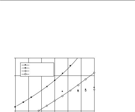
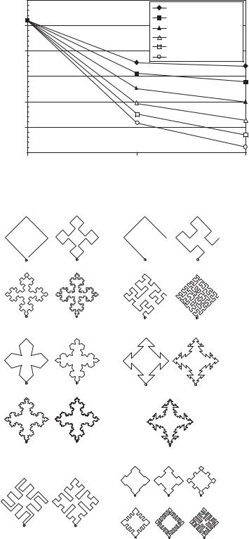
A Meander line pattern is the simplest one to fill a space of given area, and has been applied in various small wireless systems. A representative pattern is that of a dipole shown in Figure 7.24, which is described in Section 7.2.1.1. Variations of the basic meander line profile from the original rectangular one are triangular profile and sinusoidal profile (Figure 7.85 N1, N2, and N3) [35]. The meander line with triangle profile raises radiation resistance from 26.5 to 120 , and the sinusoidal profile meander line significantly reduces resonance frequency from 543 MHz to 325 MHz, indicating a comparable reduction of antenna size. These parameters are listed in Table 7.7, where resonance frequency, radiation resistance, Q, and the size are provided.
In order to use space more efficiently and improve antenna performances, further modification of meander line profile are taken into consideration by taking various geometries shown in Figure 7.86, where four types, M1 through M4, are illustrated. Performances were studied and found lower resonance frequency with smaller size, moderate value of Q, and lower cross polarization level, although radiation resistance decreases (Table 7.8). Meandered wire itself can be a meandered structure to further lower the resonance frequency so that the antenna size can be reduced.
Some types of planar meandered antennas used in mobile phones will be introduced as examples of practical applications in later sections. Examples of other types of planar meandered antennas developed for RFID tags were a meandered rectangular loop

144 |
Design and practice of small antennas I |
|
|
Table 7.8 |
Parameters of meander line patterns of four different types; M1, M2, M3, and M4 [35] |
|||||||||||||||||||||||||||||||||
|
|
|
|
|
|
|
|
|
|
|
|
|
|
|
|
|
|
|
|
|
|
|
|
|
|
|
|
|
|
|
|
|
|
|
|
Radiation |
|
|
Resonant |
|
|
|
|
|
|
|
|
|
|
|
|
|
|
|
|
||||||||||||||
Antennas |
resistance ( ) |
|
|
frequency (MHz) |
ka |
Q |
QChu |
|
Cross-Pol. (dB) |
|||||||||||||||||||||||||
M1 |
11.68 |
|
|
512.92 |
|
|
|
|
|
|
|
0.645 |
114.2 |
5.277 |
|
|
−115.9 |
|||||||||||||||||
M2 |
18.32 |
|
|
474.5 |
|
|
|
|
|
|
|
|
0.67 |
66.25 |
4.871 |
|
|
−118.6 |
||||||||||||||||
M3 |
15.7 |
|
|
423.9 |
|
|
|
|
|
|
|
|
0.6 |
102.5 |
6.296 |
|
|
−117.1 |
||||||||||||||||
M4 |
5.89 |
|
|
414.95 |
|
|
|
|
|
|
|
0.588 |
54.39 |
6.62 |
|
|
|
−122.7 |
||||||||||||||||
|
|
|
|
|
|
|
|
|
|
|
|
|
|
|
|
|
|
|
|
|
|
|
|
|
|
|
|
|
|
|
|
|
|
|
|
|
|
|
|
|
|
|
|
|
|
|
|
|
|
|
|
|
|
|
|
|
|
|
|
|
|
|
|
|
|
|
|
|
|
|
|
|
|
|
|
|
|
|
|
|
|
|
|
|
|
|
|
|
|
|
|
|
|
|
|
|
|
|
|
|
|
|
|
|
|
|
|
|
|
|
|
|
|
|
|
|
|
|
|
|
|
|
|
|
|
|
|
|
|
|
|
|
|
|
|
|
|
|
|
|
|
|
|
|
|
|
|
|
|
|
|
|
|
|
|
|
|
|
|
|
|
|
|
|
|
|
|
|
|
|
|
|
|
|
|
|
|
|
|
|
|
|
|
|
|
|
|
|
|
|
|
|
|
|
|
|
|
|
|
|
|
|
|
|
|
|
|
|
|
|
|
|
|
|
|
|
|
|
|
|
|
|
|
|
|
|
|
|
|
|
|
|
|
|
|
|
|
|
|
|
|
|
|
|
|
|
|
|
|
|
|
|
|
|
|
|
|
|
|
|
|
|
|
|
|
|
|
|
|
|
|
|
|
|
|
|
|
|
|
|
|
|
|
|
|
|
|
|
|
|
|
|
|
|
|
|
|
|
|
|
|
|
|
|
|
|
|
|
|
|
|
|
|
|
|
|
|
|
|
|
|
|
|
|
|
|
|
|
|
|
|
|
|
|
|
|
|
|
|
|
|
|
|
|
|
|
|
|
|
|
|
|
|
|
|
|
|
|
|
|
|
|
|
|
|
|
|
|
|
|
|
|
|
|
|
|
|
|
|
|
|
|
|
|
|
|
|
|
|
|
|
|
|
|
|
|
|
|
|
|
|
|
|
|
|
|
|
|
|
|
|
|
|
|
|
|
|
|
|
|
|
|
|
|
|
|
|
|
|
|
|
|
|
|
|
|
|
|
|
|
|
|
|
|
|
|
|
|
|
|
|
|
|
|
M1 |
M2 |
M3 |
M4 |
Figure 7.86 Variation of meander line patterns: M1, M2, M3, and M4 ([35], copyright C 2009 IEEE).
[36] and a C-shaped folded monopole structure [37], operating at 900-MHz band and 400-MHz bands, respectively.
7.2.2.1.2 Koch Fractal curve, Peano curve and Hilbert curve 7.2.2.1.2.1 Monopole using Koch, Peano, and Hilbert curves
It is well known that use of space-filling geometry, such as Koch, Peano, and Hilbert curves [38–42] for antenna structure to lengthen the antenna in a given space so that the resonance frequency is lowered, results in small-sizing of an antenna. It is also useful for obtaining wideband or multiband operation with small antennas, as the wire length (stretched straight) increases with number of iterations of initial geometry.
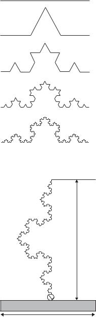
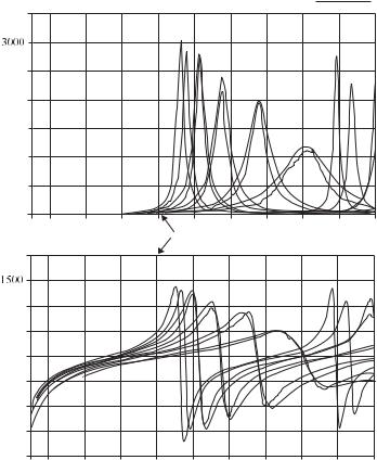
A Koch monopole is generated by an iterative procedure that repeats replacing one third of the line at its center with an equilateral triangle, then scaling and rotating it infinitely as shown in Figure 7.87, which depicts the generator of the pattern and iteration process [38]. A Koch monopole having height h = 6 cm, being placed over the 80-cm ground plane is illustrated in Figure 7.88. The computed and measured input impedances with respect to number n of the iteration are shown in Figure 7.89, where
(a) is the resistance and (b) is the reactance. The stretched length l of the antenna is expressed by l = h (4/3)n and an antenna constructed by iteration of n times is denoted as Kn, where n = 0 means the Euclidean version of the antenna, that is an ordinary straight monopole. A line expressing the small-antenna limit kh < 1 is drawn as the
7.2 Design and practice of ESA |
145 |
|
|
K0
K 1
K 2
K3
K4
Figure 7.87 Koch monopole structures; generator K0 through fourth stage K4, ([38], copyrightC 2000 IEEE).
6 cm
80 cm
Figure 7.88 Koch monopole antenna of the fourth stage ([38], copyright C 2000 IEEE).
reference. The figure indicates that the resonance frequency is lowered with increase in n, resulting in reduced sizing of the antenna corresponding to the lowered frequency.
The Koch Fractal monopole is considered to be useful for lowering resonance frequency and thus small-sizing an antenna. However, comparison with two other types
146 |
Design and practice of small antennas I |
|
|
(a) |
3500 |
|
(Ω) |
2500 |
|
resistance |
2000 |
|
|
||
Input |
1500 |
|
1000 |
||
|
500 |
|
|
0 |
|
(b) |
2000 |
|
Ω) |
1000 |
|
|
||
( |
500 |
|
reactance |
||
0 |
||
|
||
Input |
−500 |
|
−1000 |
||
|
−1500
−2000
Experimental |
|
Computed (MoM) |
|
K5 K4
K3
K 2
K1
K0
0.2 |
0.4 |
0.6 |
0.8 |
1.0 |
1.2 |
1.4 |
1.6 |
1.8 |
2.0 |
|
|
|
|
Small antenna limit, kh<1 |
|
|
|||
K0
K1
K3 K2
K5 K4
0.2 |
0.4 |
0.6 |
0.8 |
1.0 |
1.2 |
1.4 |
1.6 |
1.8 |
2.0 |
f (GHz)
Figure 7.89 Input impedance of different stage of Koch monopole: (a) resistance and (b) reactance ([38], copyright C 2000 IEEE).
of wire antennas, meander line antenna (MLA) and helical antenna (NMHA), reveals that the Koch Fractal antenna has relatively higher resonance frequency compared with that of MLA and NMHA (Figure 7.90) [39], for the same (stretched) wire length l. This means that when the resonance frequency is adjusted to be equal for the three types of antenna, keeping the antenna height h the same, the wire length l of the Koch Fractal monopole becomes the longest among these three types of antenna, while the antenna performances, radiation resistance, and the bandwidth, are about the same, as Table 7.9 shows [39].
This fact suggests that the antenna specific geometry is not necessarily significant for small-sizing of an antenna, but the electrical length, not physical length, is essential.
Instead of a single wire structure, a given space is filled more efficiently by single Peano or Hilbert curve elements. Consider these two curve structures, Peano and Hilbert, previously illustrated in Figure 7.81 (a) and (b), respectively, embedded in a square of 3 × 3 cm [41]. Induced currents due to normally incident plane waves for these
7.2 Design and practice of ESA |
147 |
|
|
Table 7.9 Comparison of antenna performances for three types at the same resonance frequency ([39], copyright C 2003 IEEE)
|
|
|
|
|
2:1 SWR |
|
Resonant |
Overall |
Total wire |
Resonant |
bandwidth |
Antennas |
frequency (MHz) |
height (cm) |
length (cm) |
resistance (ohms) |
(%) |
|
|
|
|
|
|
K0 |
1201 |
6 |
6 |
36.8 |
8.5 |
K3 |
745.3 |
6 |
14.22 |
15.4 |
3.5 |
M3 |
745.3 |
6 |
12.32 |
15.6 |
3.5 |
H3 |
745.3 |
6 |
11.46 |
15.8 |
3.5 |
|
|
|
|
|
|
Resonant frequency (MHz)
1250
1050
850
Koch Fractal
650
Meander
450
Helix
Euclidean
250
0 |
1 |
2 |
3 |
4 |
5 |
Antenna iteration
Figure 7.90 Comparison of resonance frequency for three types of antenna in terms of iteration number ([39], copyright C 2003 IEEE).
structures differ depending on the curve structure and direction of the incident wave. Subsequently, resonance frequency differs depending on the polarization of the incident wave and relates with the electrical length of wire (stretched) residing in the square. For instance, for the horizontally polarized incidence wave the resonance frequency of the Peano curve structure is about one third of that for the vertical polarization incidence, because the electrical wire length is longer in the horizontally polarized wave than that of the vertically polarized wave. The antenna performance of the Hilbert curve structure is similar to that of the Peano curve structure. A Peano curve can fill a space much more than a Hilbert curve for the same number of iterations. This can be understood from Table 7.10.
The Peano curve structure is applied to an antenna of a dipole type as shown in Figure 7.91, in which the feed point is shown as an example [41].
In the same way, the Hilbert curve structure is applied to a dipole type as shown in Figure 7.92 [42]. Input impedance of the 2nd-order Hilbert structure is illustrated in
148 |
Design and practice of small antennas I |
|
|
Table 7.10 Total length (stretched) S for Peano and Hilbert curves with respect to the iteration number ([40], copyright C 2006 John Wiley and Sons Inc.)
|
2N |
− 1)d |
N |
− 1) |
Peano |
S = (32N |
d = L/(3N |
||
Hilbert |
S = (2 |
− 1)d |
d = L/(2 |
− 1) |
Note: L is the linear side dimension of the curve.
Feed point |
Feed point |
Feed point |
n = 1 |
n = 2 |
n = 3 |
Figure 7.91 Peano dipoles, orders n = 1 through 3 ([41], copyright C 2004 IEEE).
(a) |
|
|
|
|
|
|
|
|
(b) |
|||||||||
|
|
|
|
|
|
|
|
|
|
|
|
|
|
|
|
|
|
|
|
|
|
|
|
|
|
|
|
|
|
|
|
|
|
|
|
|
|
|
|
|
|
|
|
|
|
|
|
|
|
|
|
|
|
|
|
|
|
|
|
|
|
|
|
|
|
|
|
|
|
|
|
|
|
|
|
|
|
|
|
|
|
|
|
|
|
|
|
|
|
|
|
|
|
|
|
|
|
|
|
|
|
|
|
|
|
|
|
|
|
|
|
|
|
|
|
|
|
|
|
|
|
|
|
|
|
|
|
|
|
|
|
|
|
|
|
|
|
|
|
|
|
|
|
|
|
|
|
|
|
|
|
|
|
|
|
|
|
|
|
|
|
|
|
|
|
|
|
|
|
|
|
|
|
|
|
|
|
|
|
|
|
|
|
|
|
|
|
|
|
|
|
|
|
|
|
|
|
|
|
|
|
|
|
|
|
|
|
|
|
|
|
|
|
|
|
|
|
|
|
|
|
|
|
|
|
|
|
|
|
|
|
|
|
|
|
|
|
|
|
|
|
|
|
|
|
|
|
|
|
|
|
|
|
|
|
|
|
|
|
|
|
|
|
|
|
|
|
|
|
|
|
|
|
|
|
|
|
|
|
|
|
|
|
|
|
|
|
|
|
|
|
|
|
|
|
|
|
|
|
|
|
|
|
|
|
|
|
|
|
|
|
|
|
|
|
|
|
|
|
|
|
|
|
|
|
|
|
|
|
|
|
|
|
|
|
|
|
|
|
|
|
|
|
|
|
|
|
|
|
|
|
|
|
|
|
|
|
|
|
|
(c) |
(d) |
Figure 7.92 Hilbert dipoles; (a) 1st order, (b) 2nd order, (c) 3rd order, and (d) fourth order ([42], copyright C 2003 IEEE).
7.2 Design and practice of ESA |
149 |
|
|
Table 7.11 Resonance frequency and input impedance of Hilbert antenna of 2nd and 3rd stages ([42], copyright C 2003 IEEE)
|
|
|
Resonant frequency by |
|
Outer |
Fractal |
Width of |
RWG MoM code with |
Impedance when |
dimension (mm) |
iteration order |
strip (mm) |
substrate (MHz) |
resonating |
|
|
|
|
|
50 |
2 |
4 |
582.087 |
3.79829 |
50 |
3 |
4 |
415.516 |
0.95505 |
80 |
2 |
4 |
371.716 |
3.93187 |
80 |
3 |
4 |
263 |
0.98539 |
80 |
2 |
8 |
385.686 |
4.26708 |
80 |
3 |
8 |
277.2 |
1.04867 |
|
|
|
|
|
Impedance (Ω)
200
Re (Z) with substrate
Im (Z) with substrate
Re (Z) w/o substrate
Im (Z) w/o substrate
100
0 


−100 |
|
|
|
|
|
|
500 |
550 |
600 |
650 |
700 |
750 |
800 |
|
|
Frequency |
|
|
(MHz) |
|
Figure 7.93 Input impedance of 2nd-order Hilbert antenna fed at the center, with and without substrate; width = 4 mm and other dimensions = 50 mm ([42], copyright C 2003 IEEE).
Figure 7.93. The input impedance can be adjusted to about 50 by selecting the feed position. Table 7.11 provides variation of resonance frequency and input impedance with respect to the iteration number, outer dimensions and width of strip. Current distributions along a 3rd-order Hilbert dipole printed on the substrate of εr = 4.3 and fed at the center at resonance frequency 582.087 MHz having the outer dimensions of 4.5 cm is shown in Figure 7.94. The current distribution is almost the same as that for the center-fed and very similar to that of a half-wave dipole resembling a sinusoidal wave, and does not vary significantly with change in the iteration number. Radiation patterns of the 3rd order Hilbert Dipole antenna is shown in Figure 7.95, which is nearly the same as that of a dipole antenna.
Figure 7.96 compares the size between a printed dipole antenna and the 2ndand the 3rd-order Hilbert dipoles. The figure shows that the 2ndand the 3rd-order Hilbert dipoles have dimensions of about 1/4 and about 2/11, respectively, of that of the dipole.
150 |
Design and practice of small antennas I |
|
|
Current density
120 |
|
|
100 |
Real |
|
Imaginary |
||
|
80
60 |
|
|
|
|
|
|
|
|
|
40 |
|
|
|
|
|
|
|
|
|
20 |
|
|
|
|
|
|
|
|
|
0 |
|
|
|
|
|
|
|
|
|
−20 |
|
|
|
|
0.25 |
0.3 |
0.35 |
0.4 |
0.45 |
0 |
0.05 |
0.1 |
0.15 |
0.2 |
Distance along antenna
Figure 7.94 Current distribution along a 3rd-order Hilbert antenna with substrate and fed at node 32 (a dot on the element) at resonance frequency (outer dimension is 4.5 cm and width is 2 mm) ([42], copyright C 2003 IEEE).
90
0.0035

135 |
|
|
45 |
|
|
|
|
|
|
0.003 |
|
|
|
|
0.0025 |
|
|
|
|
0.002 |
|
|
|
|
0.001 |
0.002 |
0.0025 |
0.003 |
0.0035 |
180 |
|
|
|
0 |
0
18
36
54
72
225 |
315 |
270
Figure 7.95 Radiation pattern of the 3rd-order Hilbert antenna with substrate fed at node 24 at the resonance frequency ([42], copyright C 2003 IEEE).
7.2.2.1.2.2 PIFA using Peano curve elements
A Peano curve structure is used for miniaturizing a PIFA element, replacing the horizontal element with planar Peano curve elements. The antenna has two planar Peano elements to cover dual bands, which are designed for applications to GSM in 900 MHz band and PCS in 1900 MHz band [43]. The geometry is shown in Figure 7.97, in which
7.2 Design and practice of ESA |
151 |
|
|
Table 7.12 Dimensions of optimized antenna shown in
Fig. 7.97 ([43], copyright C 2006 IEICE)
|
P1 |
L1 |
s |
x1 |
x2 |
x3 |
A |
34.4 |
14.3 |
6 |
4.6 |
– |
5.4 |
B |
32.9 |
13 |
6 |
5.1 |
1.2 |
– |
C |
40 |
12.5 |
7.7 |
5.6 |
4.5 |
5.1 |
|
|
|
|
|
|
|
Dimension of antenna (mm)
500 |
|
|
|
450 |
|
|
|
400 |
|
Dipole |
|
350 |
|
Hilbert order 2 |
|
|
Hilbert order 3 |
|
|
|
|
|
|
300 |
|
|
|
250 |
|
|
|
200 |
|
|
|
150 |
|
|
|
100 |
|
|
|
50 |
|
|
|
0 |
500 |
700 |
900 |
300 |
|||
|
Resonance frequency |
(MHz) |
|
Figure 7.96 Comparison of the dimension of printed dipole and Hilbert antenna at the same resonance frequency ([42], copyright C 2003 IEEE).
|
P1 |
L1 |
|
|
Feed |
x3 |
|
||
s |
z |
|||
|
|
x2 x1 |
y |
|
|
|
|
|
x |
|
|
Lg |
|
|
Shorting |
|
|||
|
|
|
||
|
pin |
Ground |
||
Figure 7.97 Dual-band 2nd-order Peano PIFA ([43], copyright C 2006 IEEE).
dimensional parameters are given. Optimized antenna dimensions are listed in Table 7.12, in which A and B give parameters for an antenna with height = 8.25 mm and C gives for that h = 8 mm and the one side element is replaced with a rectangular patch. Computed VSWR of the antenna in the 900 MHz band and that of the antenna in the 1900 MHz band are illustrated in Figures 7.98 and 7.99, respectively. By using a Peano element, the PIFA can be miniaturized about 50% in volume compared with a conventional PIFA.
152 |
Design and practice of small antennas I |
|
|
VSWR
5 |
|
|
4.5 |
|
|
4 |
|
|
3.5 |
Antenna B |
|
3 |
|
|
|
|
|
2.5 |
|
|
2 |
|
|
1.5 |
Antenna A |
Antenna C |
|
|
1
880 900 920 940 960 980 1000 1020
Frequency (MHz)
Figure 7.98 Computed VSWR for antennas A, B, and C near 900 MHz band ([43], copyrightC 2006 IEEE).
VSWR
5
4.5
4
3.5
3
Antenna B
2.5
2 |
Antenna A |
Antenna C
1.5
1
1840 1860 1880 1900 1920 1940 1960 1980 2000
Frequency (MHz)
Figure 7.99 Computed VSWR for antenna A, B, and C near 1920 MHz band ([43], copyrightC 2006 IEEE).
7.2.2.1.3 Minkowsky and Sierpinsky Fractal monopoles 7.2.2.1.3.1 Planar Minkowsky Fractal monopole
A Minkowsky Fractal monopole is generated starting from a Euclidean square by replacing each of the four segments of the initial square with the generator shown, and repeating it for an infinite number of times as illustrated in Figure 7.100 [44], which shows only from the initiator to the third iteration structure. To utilize space-filling ability, a firstorder planar Minkowsky loop is fabricated (Figure 7.101) and its performances are reported [44]. The perimeter length lp is given by
lpn = (1 + 2w/3)nlp(n−1) |
(7.59) |
7.2 Design and practice of ESA |
153 |
|
|
Initiator
> Indentation width
Generator
Figure 7.100 Iterative generation procedure for Minkowsky island fractal; transition from a generator is shown below ([44], copyright C 2002 IEEE).
Figure 7.101 The first-order Minkowsky fractal loop antenna ([44], copyright C 2002 IEEE).
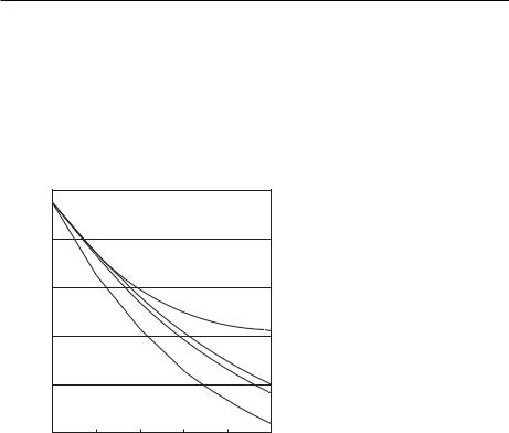
where n is the iteration number and w is the indentation width. Scaling factor for resonance for a λ/4 square loop for various numbers of iteration and for varying indentation widths is shown in Figure 7.102, which provides design curves for resonance frequency with respect to number of iteration and indentation width. The resonance frequency is reduced as the iteration number increases and the indentation number as well.
7.2.2.1.3.2 Comparison of planar Minkowsky fractal monopoles with other space-filling-curve monopoles [45]
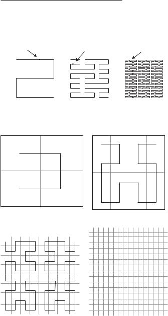
Planar monopoles using various space-filling curves such as (a) Minkowsky fractal,
(b) Hilbert curve, (c) Koch fractal, (d) tee-fractal, (e) box-meander line, and (f) meander line, having planar area of 15.7 cm × 15.7 cm (246.5 cm2), respectively are shown in Figure 7.103(a), (b), (c), (d), (e), and (f). The physical and resonance properties are
|
1.2 |
|
Indentation width = 0.200 |
|
|
|
|
/4 |
|
|
Indentation width = 0.333 |
λ |
1.1 |
|
Indentation width = 0.500 |
for |
|
||
|
|
Indentation width = 0.666 |
|
factorfor resonance |
|
|
|
1 |
|
Indentation width = 0.800 |
|
|
Indentation width = 0.900 |
||
|
|
||
0.9 |
|
|
|
0.8 |
|
|
|
loopsquare |
|
|
|
Scaling |
0.7 |
|
|
|
|
|
|
|
0.6 |
|
|
|
0 |
1 |
2 |
Fractal iteration
Figure 7.102 Scaling factor for design of Minkowsky loop antenna for various indentation width in terms of iteration number ([44], copyright C 2002 IEEE).
(a) |
M0 |
M1 |
(b) |
H0 |
H1 |
|
|
|
|
M2 |
M3 |
H2 |
H3 |
K1 |
K2 |
|
T 1 |
T 2 |
(c) |
|
(d) |
||
|
|
|
K3 |
K4 |
T 3 |
|
|
(e) |
(f ) |
ML2 ML3 ML4 |
|
B-1 B-2
ML5 ML6 ML7
Figure 7.103 Various types of planar fractal monopole: (a) mod-Minkowsky fractal, (b) Hilbert curve fractal, (c) Koch fractal, (d) tee-fractal, (e) box-meander line, and (f) meander line ([45], copyright C 2003 IEEE).
7.2 Design and practice of ESA |
155 |
|
|
(a) |
|
Hilbert curve |
|
|
|
|
|
|
|
|
|
|
|
|
|
||
(ohms) |
12 |
Mod-Minkowski |
|
|
|
|
|
|
Koch curve |
|
|
|
|
|
|
||
|
|
|
|
|
|
|
||
+ |
Tee fractal |
|
|
|
|
|
|
|
Box meander |
|
|
|
|
|
|||
|
Meander line |
|
|
|
|
|
||
|
|
|
|
|
|
|
|
|
resistance |
8 |
|
|
|
|
|
|
|
|
|
|
|
|
|
|
|
|
Radiation |
4 |
|
|
|
|
|
|
|
|
|
+ |
|
|
|
|
|
|
0 |
|
|
|
|
|
|
|
|
|
|
|
|
|
|
|
|
|
|
40 |
60 |
80 |
100 |
120 |
140 |
160 |
180 |
Resonant frequency (MHz)
(b) |
|
|
|
|
|
Hilbert curve |
|
|
600 |
|
|
|
|
|
|
||
|
|
|
|
|
Mod-Minkowski |
|
||
|
|
|
|
|
|
Koch curve |
|
|
|
|
|
|
|
+ |
Tee fractal |
|
|
|
|
|
|
|
Box meander |
|
||
|
|
|
|
|
|
Meander line |
|
|
400 |
|
|
|
|
|
|
|
|
Q |
|
|
|
|
|
|
|
|
200 |
|
++ |
|
|
|
|
|
|
|
|
|
|
|
|
|
|
|
0 |
|
|
|
|
|
|
|
|
40 |
60 |
80 |
100 |
120 |
140 |
160 |
180 |
|
Resonant frequency (MHz)
Figure 7.104 Radiation resistance and Q of six types of planar monopoles shown in Figure 7.103:
(a) radiation resistance and (b) Q ([46], copyright C 2009 IEEE).
compared in terms of resonance frequency, radiation resistance, efficiency, and Q for various iteration numbers. Radiation resistance and Q of these antennas are illustrated in Figure 7.104(a) and (b), respectively. The analysis disclosed that there are no significant differences in the resonance properties of these antennas, although antenna geometry and total wire length differ, indicating that their resonance behavior is primarily established by their occupied area [45]. This analysis provides useful suggestions for designing planar monopoles using space-filling curves.
7.2.2.1.3.3 Sierpinsky Fractal monopole
Sierpinsky Fractal structures (Figure 7.105 [46, 47]) were discovered by W. Sierpinsky in 1916. The Sierpinsky Fractal is generated starting from an equilateral triangle by removing the central triangle with vertices located at the midpoints of the sides of the original triangle, and repeating it for the three remaining triangles and then nine

156 |
Design and practice of small antennas I |
|
|
Figure 7.105 Sierpinsky fractal structure ([47], copyright C 2003 IEEE).
n = 0 |
n = 1 |
n = 2 |
n = 3 |
n = 4 |
Figure 7.106 The first four stages in construction of a conventional Sierpinsky gasket fractal ([47], copyright C 2003 IEEE).
S11 (dB)
0 |
|
|
|
|
|
|
|
|
−10 |
|
|
|
|
|
|
|
|
−20 |
|
|
|
|
Measurements |
|
|
|
|
|
|
|
Simulations |
|
|
||
|
|
|
|
|
|
|
||
0 |
2 |
4 |
6 |
8 |
10 |
12 |
14 |
16 |
f (GHz)
Figure 7.107 Return-loss characteristics relative to 50 ([47], copyright C 2003 IEEE).
remaining triangles, and so on to form a sieve of triangles as shown in Figure 7.105 [46]. The Sierpinsky sieve (or gasket) of triangles is, when applied to an antenna structure, characterized by a certain multiband behavior owing to its self-similar shape. A monopole antenna based on the Sierpinsky gasket has been shown to be an excellent candidate for multiband applications. The simulated and measured input reflection coefficient (S11) of a four-stage Sierpinsky structure (Figure 7.106) is depicted in Figure 7.107 [46]. The antenna dimensions are: height h = 88.9, hn/hn+1 = 2, flare angle α = 60◦, thickness of the substrate hs = 1.588, permittivity εr = 2.5, and the iteration number n = 4 (in mm for all dimensional parameters). The antenna parameters are provided in Table 7.13, in which frequency band, resonance frequency, bandwidth, reflection coefficient, ratio of iteration segment, and height of triangle for each segment in terms of wavelength, are provided. A five-order Sierpinsky monopole shown in Figure 7.108 [47] was fabricated and measured and the simulated reflection coefficient is shown in Figure 7.109
7.2 Design and practice of ESA |
157 |
|
|
Table 7.13 Sierpinsky gasket fractal monopole parameters ([46], copyright C 2009 IEEE, and [47], copyright C 2003 IEICE)
|
Band |
|
|
|
|
|
Iteration |
number |
S11 fm [GHz] |
Bandwidth [%] |
[dB] |
frn+1/ frn |
hn /λn |
0 |
1 |
0.52 |
7.15 |
10 |
3.50 |
0.153 |
1 |
2 |
1.74 |
9.04 |
14 |
2.02 |
0.258 |
2 |
3 |
3.51 |
20.5 |
24 |
1.98 |
0.261 |
3 |
4 |
6.95 |
22 |
19 |
2.00 |
0.257 |
4 |
5 |
13.89 |
25 |
20 |
– |
0.255 |
|
|
|
|
|
|
|
z
 y
y
x
cm 89.8
|
|
|
|
cm 45.4 |
|
|
|
2 |
|
cm 55.0 |
|
cm 11.1 |
cm 23. |
|
|
|
|||
|
|
|
|
|
80 cm
Figure 7.108 A five-order Sierpinsky monopole ([47], copyright C 2003 IEEE).
|
0 |
|
|
|
(dB) |
−10 |
|
|
|
|
|
|
|
|
in |
|
|
|
|
Γ |
−20 |
|
|
|
|
|
|
|
|
|
|
|
|
Experiment |
|
−30 |
|
|
Simulation |
|
|
|
|
|
|
1 |
2 |
4 |
8 |
f (GHz)
Figure 7.109 Input reflection coefficient relative to 50 ([47], copyright C 2003 IEEE).