

- •Contents
- •List of Tables
- •List of Figures
- •Preface
- •About this manual
- •Product revision status
- •Intended audience
- •Using this manual
- •Conventions
- •Additional reading
- •Feedback
- •Feedback on the product
- •Feedback on this book
- •Introduction
- •1.1 About the processor
- •1.2 Extensions to ARMv6
- •1.3 TrustZone security extensions
- •1.4.1 Instruction compression
- •1.4.2 The Thumb instruction set
- •1.4.3 Java bytecodes
- •1.5 Components of the processor
- •1.5.1 Integer core
- •1.5.2 Load Store Unit (LSU)
- •1.5.3 Prefetch unit
- •1.5.4 Memory system
- •1.5.5 AMBA AXI interface
- •1.5.6 Coprocessor interface
- •1.5.7 Debug
- •1.5.8 Instruction cycle summary and interlocks
- •1.5.9 System control
- •1.5.10 Interrupt handling
- •1.6 Power management
- •1.7 Configurable options
- •1.8 Pipeline stages
- •1.9 Typical pipeline operations
- •1.9.1 Instruction progression
- •1.10.1 Extended ARM instruction set summary
- •1.10.2 Thumb instruction set summary
- •1.11 Product revisions
- •Programmer’s Model
- •2.1 About the programmer’s model
- •2.2.1 TrustZone model
- •2.2.2 How the Secure model works
- •2.2.3 TrustZone write access disable
- •2.2.4 Secure Monitor bus
- •2.3 Processor operating states
- •2.3.1 Switching state
- •2.3.2 Interworking ARM and Thumb state
- •2.4 Instruction length
- •2.5 Data types
- •2.6 Memory formats
- •2.7 Addresses in a processor system
- •2.8 Operating modes
- •2.9 Registers
- •2.9.1 The ARM state core register set
- •2.9.2 The Thumb state core register set
- •2.9.3 Accessing high registers in Thumb state
- •2.9.4 ARM state and Thumb state registers relationship
- •2.10 The program status registers
- •2.10.1 The condition code flags
- •2.10.2 The Q flag
- •2.10.4 The GE[3:0] bits
- •2.10.7 The control bits
- •2.10.8 Modification of PSR bits by MSR instructions
- •2.10.9 Reserved bits
- •2.11 Additional instructions
- •2.11.1 Load or Store Byte Exclusive
- •2.11.2 Load or Store Halfword Exclusive
- •2.11.3 Load or Store Doubleword
- •2.11.4 CLREX
- •2.12 Exceptions
- •2.12.1 New instructions for exception handling
- •2.12.2 Exception entry and exit summary
- •2.12.3 Entering an ARM exception
- •2.12.4 Leaving an ARM exception
- •2.12.5 Reset
- •2.12.6 Fast interrupt request
- •2.12.7 Interrupt request
- •2.12.8 Low interrupt latency configuration
- •2.12.9 Interrupt latency example
- •2.12.10 Aborts
- •2.12.11 Imprecise Data Abort mask in the CPSR/SPSR
- •2.12.12 Supervisor call instruction
- •2.12.13 Secure Monitor Call (SMC)
- •2.12.14 Undefined instruction
- •2.12.15 Breakpoint instruction (BKPT)
- •2.12.16 Exception vectors
- •2.12.17 Exception priorities
- •2.13 Software considerations
- •2.13.1 Branch Target Address Cache flush
- •2.13.2 Waiting for DMA to complete
- •System Control Coprocessor
- •3.1 About the system control coprocessor
- •3.1.1 System control coprocessor functional groups
- •3.1.2 System control and configuration
- •3.1.3 MMU control and configuration
- •3.1.4 Cache control and configuration
- •3.1.5 TCM control and configuration
- •3.1.6 Cache Master Valid Registers
- •3.1.7 DMA control
- •3.1.8 System performance monitor
- •3.1.9 System validation
- •3.1.10 Use of the system control coprocessor
- •3.2 System control processor registers
- •3.2.1 Register allocation
- •3.2.2 c0, Main ID Register
- •3.2.3 c0, Cache Type Register
- •3.2.4 c0, TCM Status Register
- •3.2.5 c0, TLB Type Register
- •3.2.6 c0, CPUID registers
- •3.2.7 c1, Control Register
- •3.2.8 c1, Auxiliary Control Register
- •3.2.9 c1, Coprocessor Access Control Register
- •3.2.10 c1, Secure Configuration Register
- •3.2.11 c1, Secure Debug Enable Register
- •3.2.13 c2, Translation Table Base Register 0
- •3.2.14 c2, Translation Table Base Register 1
- •3.2.15 c2, Translation Table Base Control Register
- •3.2.16 c3, Domain Access Control Register
- •3.2.17 c5, Data Fault Status Register
- •3.2.18 c5, Instruction Fault Status Register
- •3.2.19 c6, Fault Address Register
- •3.2.20 c6, Watchpoint Fault Address Register
- •3.2.21 c6, Instruction Fault Address Register
- •3.2.22 c7, Cache operations
- •3.2.23 c8, TLB Operations Register
- •3.2.24 c9, Data and instruction cache lockdown registers
- •3.2.25 c9, Data TCM Region Register
- •3.2.26 c9, Instruction TCM Region Register
- •3.2.29 c9, TCM Selection Register
- •3.2.30 c9, Cache Behavior Override Register
- •3.2.31 c10, TLB Lockdown Register
- •3.2.32 c10, Memory region remap registers
- •3.2.33 c11, DMA identification and status registers
- •3.2.34 c11, DMA User Accessibility Register
- •3.2.35 c11, DMA Channel Number Register
- •3.2.36 c11, DMA enable registers
- •3.2.37 c11, DMA Control Register
- •3.2.38 c11, DMA Internal Start Address Register
- •3.2.39 c11, DMA External Start Address Register
- •3.2.40 c11, DMA Internal End Address Register
- •3.2.41 c11, DMA Channel Status Register
- •3.2.42 c11, DMA Context ID Register
- •3.2.44 c12, Monitor Vector Base Address Register
- •3.2.45 c12, Interrupt Status Register
- •3.2.46 c13, FCSE PID Register
- •3.2.47 c13, Context ID Register
- •3.2.48 c13, Thread and process ID registers
- •3.2.49 c15, Peripheral Port Memory Remap Register
- •3.2.51 c15, Performance Monitor Control Register
- •3.2.52 c15, Cycle Counter Register
- •3.2.53 c15, Count Register 0
- •3.2.54 c15, Count Register 1
- •3.2.55 c15, System Validation Counter Register
- •3.2.56 c15, System Validation Operations Register
- •3.2.57 c15, System Validation Cache Size Mask Register
- •3.2.58 c15, Instruction Cache Master Valid Register
- •3.2.59 c15, Data Cache Master Valid Register
- •3.2.60 c15, TLB lockdown access registers
- •Unaligned and Mixed-endian Data Access Support
- •4.2 Unaligned access support
- •4.2.1 Legacy support
- •4.2.2 ARMv6 extensions
- •4.2.3 Legacy and ARMv6 configurations
- •4.2.4 Legacy data access in ARMv6 (U=0)
- •4.2.5 Support for unaligned data access in ARMv6 (U=1)
- •4.2.6 ARMv6 unaligned data access restrictions
- •4.3 Endian support
- •4.3.1 Load unsigned byte, endian independent
- •4.3.2 Load signed byte, endian independent
- •4.3.3 Store byte, endian independent
- •4.4 Operation of unaligned accesses
- •4.5.1 Legacy fixed instruction and data endianness
- •4.5.3 Reset values of the U, B, and EE bits
- •4.6.1 All load and store operations
- •4.7 Instructions to change the CPSR E bit
- •Program Flow Prediction
- •5.1 About program flow prediction
- •5.2 Branch prediction
- •5.2.1 Enabling program flow prediction
- •5.2.2 Dynamic branch predictor
- •5.2.3 Static branch predictor
- •5.2.4 Branch folding
- •5.2.5 Incorrect predictions and correction
- •5.3 Return stack
- •5.4 Memory Barriers
- •5.4.1 Instruction Memory Barriers (IMBs)
- •5.5.1 Execution of IMB instructions
- •Memory Management Unit
- •6.1 About the MMU
- •6.2 TLB organization
- •6.2.1 MicroTLB
- •6.2.2 Main TLB
- •6.2.3 TLB control operations
- •6.2.5 Supersections
- •6.3 Memory access sequence
- •6.3.1 TLB match process
- •6.3.2 Virtual to physical translation mapping restrictions
- •6.4 Enabling and disabling the MMU
- •6.4.1 Enabling the MMU
- •6.4.2 Disabling the MMU
- •6.4.3 Behavior with MMU disabled
- •6.5 Memory access control
- •6.5.1 Domains
- •6.5.2 Access permissions
- •6.5.3 Execute never bits in the TLB entry
- •6.6 Memory region attributes
- •6.6.1 C and B bit, and type extension field encodings
- •6.6.2 Shared
- •6.6.3 NS attribute
- •6.7 Memory attributes and types
- •6.7.1 Normal memory attribute
- •6.7.2 Device memory attribute
- •6.7.3 Strongly Ordered memory attribute
- •6.7.4 Ordering requirements for memory accesses
- •6.7.5 Explicit Memory Barriers
- •6.7.6 Backwards compatibility
- •6.8 MMU aborts
- •6.8.1 External aborts
- •6.9 MMU fault checking
- •6.9.1 Fault checking sequence
- •6.9.2 Alignment fault
- •6.9.3 Translation fault
- •6.9.4 Access bit fault
- •6.9.5 Domain fault
- •6.9.6 Permission fault
- •6.9.7 Debug event
- •6.10 Fault status and address
- •6.11 Hardware page table translation
- •6.11.2 ARMv6 page table translation subpage AP bits disabled
- •6.11.3 Restrictions on page table mappings page coloring
- •6.12 MMU descriptors
- •Level One Memory System
- •7.1 About the level one memory system
- •7.2 Cache organization
- •7.2.1 Features of the cache system
- •7.2.2 Cache functional description
- •7.2.3 Cache control operations
- •7.2.4 Cache miss handling
- •7.2.5 Cache disabled behavior
- •7.2.6 Unexpected hit behavior
- •7.3.1 TCM behavior
- •7.3.2 Restriction on page table mappings
- •7.3.3 Restriction on page table attributes
- •7.5 TCM and cache interactions
- •7.5.1 Overlapping between TCM regions
- •7.5.2 DMA and core access arbitration
- •7.5.3 Instruction accesses to TCM
- •7.5.4 Data accesses to the Instruction TCM
- •7.6 Write buffer
- •Level Two Interface
- •8.1 About the level two interface
- •8.1.1 AXI parameters for the level 2 interconnect interfaces
- •8.2 Synchronization primitives
- •8.2.3 Example of LDREX and STREX usage
- •8.3 AXI control signals in the processor
- •8.3.1 Channel definition
- •8.3.2 Signal name suffixes
- •8.3.3 Address channel signals
- •8.4 Instruction Fetch Interface transfers
- •8.4.1 Cacheable fetches
- •8.4.2 Noncacheable fetches
- •8.5 Data Read/Write Interface transfers
- •8.5.1 Linefills
- •8.5.2 Noncacheable LDRB
- •8.5.3 Noncacheable LDRH
- •8.5.4 Noncacheable LDR or LDM1
- •8.5.5 Noncacheable LDRD or LDM2
- •8.5.6 Noncacheable LDM3
- •8.5.7 Noncacheable LDM4
- •8.5.8 Noncacheable LDM5
- •8.5.9 Noncacheable LDM6
- •8.5.10 Noncacheable LDM7
- •8.5.11 Noncacheable LDM8
- •8.5.12 Noncacheable LDM9
- •8.5.13 Noncacheable LDM10
- •8.5.14 Noncacheable LDM11
- •8.5.15 Noncacheable LDM12
- •8.5.16 Noncacheable LDM13
- •8.5.17 Noncacheable LDM14
- •8.5.18 Noncacheable LDM15
- •8.5.19 Noncacheable LDM16
- •8.6 Peripheral Interface transfers
- •8.7 Endianness
- •8.8 Locked access
- •Clocking and Resets
- •9.1 About clocking and resets
- •9.2 Clocking and resets with no IEM
- •9.2.1 Processor clocking with no IEM
- •9.2.2 Reset with no IEM
- •9.3 Clocking and resets with IEM
- •9.3.1 Processor clocking with IEM
- •9.3.2 Reset with IEM
- •9.4 Reset modes
- •9.4.1 Power-on reset
- •9.4.2 CP14 debug logic
- •9.4.3 Processor reset
- •9.4.4 DBGTAP reset
- •9.4.5 Normal operation
- •Power Control
- •10.1 About power control
- •10.2 Power management
- •10.2.1 Run mode
- •10.2.2 Standby mode
- •10.2.3 Shutdown mode
- •10.2.4 Dormant mode
- •10.2.5 Communication to the Power Management Controller
- •10.3 Intelligent Energy Management
- •10.3.1 Purpose of IEM
- •10.3.2 Structure of IEM
- •10.3.3 Operation of IEM
- •Coprocessor Interface
- •11.1 About the coprocessor interface
- •11.2 Coprocessor pipeline
- •11.2.1 Coprocessor instructions
- •11.2.2 Coprocessor control
- •11.2.3 Pipeline synchronization
- •11.2.4 Pipeline control
- •11.2.5 Instruction tagging
- •11.2.6 Flush broadcast
- •11.3 Token queue management
- •11.3.1 Queue implementation
- •11.3.2 Queue modification
- •11.3.3 Queue flushing
- •11.4 Token queues
- •11.4.1 Instruction queue
- •11.4.2 Length queue
- •11.4.3 Accept queue
- •11.4.4 Cancel queue
- •11.4.5 Finish queue
- •11.5 Data transfer
- •11.5.1 Loads
- •11.5.2 Stores
- •11.6 Operations
- •11.6.1 Normal operation
- •11.6.2 Cancel operations
- •11.6.3 Bounce operations
- •11.6.4 Flush operations
- •11.6.5 Retirement operations
- •11.7 Multiple coprocessors
- •11.7.1 Interconnect considerations
- •11.7.2 Coprocessor selection
- •11.7.3 Coprocessor switching
- •Vectored Interrupt Controller Port
- •12.1 About the PL192 Vectored Interrupt Controller
- •12.2 About the processor VIC port
- •12.2.1 Synchronization of the VIC port signals
- •12.2.2 Interrupt handler exit
- •12.3 Timing of the VIC port
- •12.3.1 PL192 VIC timing
- •12.3.2 Core timing
- •12.4 Interrupt entry flowchart
- •Debug
- •13.1 Debug systems
- •13.1.1 The debug host
- •13.1.2 The protocol converter
- •13.1.3 The processor
- •13.2 About the debug unit
- •13.2.3 Secure Monitor mode and debug
- •13.2.4 Virtual addresses and debug
- •13.2.5 Programming the debug unit
- •13.3 Debug registers
- •13.3.1 Accessing debug registers
- •13.3.2 CP14 c0, Debug ID Register (DIDR)
- •13.3.3 CP14 c1, Debug Status and Control Register (DSCR)
- •13.3.4 CP14 c5, Data Transfer Registers (DTR)
- •13.3.5 CP14 c6, Watchpoint Fault Address Register (WFAR)
- •13.3.6 CP14 c7, Vector Catch Register (VCR)
- •13.3.10 CP14 c112-c113, Watchpoint Control Registers (WCR)
- •13.3.11 CP14 c10, Debug State Cache Control Register
- •13.3.12 CP14 c11, Debug State MMU Control Register
- •13.4 CP14 registers reset
- •13.5 CP14 debug instructions
- •13.5.1 Executing CP14 debug instructions
- •13.6 External debug interface
- •13.7 Changing the debug enable signals
- •13.8 Debug events
- •13.8.1 Software debug event
- •13.8.2 External debug request signal
- •13.8.3 Halt DBGTAP instruction
- •13.8.4 Behavior of the processor on debug events
- •13.8.5 Effect of a debug event on CP15 registers
- •13.9 Debug exception
- •13.10 Debug state
- •13.10.1 Behavior of the PC in Debug state
- •13.10.2 Interrupts
- •13.10.3 Exceptions
- •13.11 Debug communications channel
- •13.12 Debugging in a cached system
- •13.12.1 Data cache writes
- •13.13 Debugging in a system with TLBs
- •13.14 Monitor debug-mode debugging
- •13.14.1 Entering the debug monitor target
- •13.14.2 Setting breakpoints, watchpoints, and vector catch debug events
- •13.14.3 Setting software breakpoint debug events (BKPT)
- •13.14.4 Using the debug communications channel
- •13.15 Halting debug-mode debugging
- •13.15.1 Entering Debug state
- •13.15.2 Exiting Debug state
- •13.15.3 Programming debug events
- •13.16 External signals
- •Debug Test Access Port
- •14.1 Debug Test Access Port and Debug state
- •14.2 Synchronizing RealView ICE
- •14.3 Entering Debug state
- •14.4 Exiting Debug state
- •14.5 The DBGTAP port and debug registers
- •14.6 Debug registers
- •14.6.1 Bypass register
- •14.6.2 Device ID code register
- •14.6.3 Instruction register
- •14.6.4 Scan chain select register (SCREG)
- •14.6.5 Scan chains
- •14.6.6 Reset
- •14.7 Using the Debug Test Access Port
- •14.7.1 Entering and leaving Debug state
- •14.7.2 Executing instructions in Debug state
- •14.7.3 Using the ITRsel IR instruction
- •14.7.4 Transferring data between the host and the core
- •14.7.5 Using the debug communications channel
- •14.7.6 Target to host debug communications channel sequence
- •14.7.7 Host to target debug communications channel
- •14.7.8 Transferring data in Debug state
- •14.7.9 Example sequences
- •14.8 Debug sequences
- •14.8.1 Debug macros
- •14.8.2 General setup
- •14.8.3 Forcing the processor to halt
- •14.8.4 Entering Debug state
- •14.8.5 Leaving Debug state
- •14.8.8 Reading the CPSR/SPSR
- •14.8.9 Writing the CPSR/SPSR
- •14.8.10 Reading the PC
- •14.8.11 Writing the PC
- •14.8.12 General notes about reading and writing memory
- •14.8.13 Reading memory as words
- •14.8.14 Writing memory as words
- •14.8.15 Reading memory as halfwords or bytes
- •14.8.16 Writing memory as halfwords/bytes
- •14.8.17 Coprocessor register reads and writes
- •14.8.18 Reading coprocessor registers
- •14.8.19 Writing coprocessor registers
- •14.9 Programming debug events
- •14.9.1 Reading registers using scan chain 7
- •14.9.2 Writing registers using scan chain 7
- •14.9.3 Setting breakpoints, watchpoints and vector traps
- •14.9.4 Setting software breakpoints
- •14.10 Monitor debug-mode debugging
- •14.10.1 Receiving data from the core
- •14.10.2 Sending data to the core
- •Trace Interface Port
- •15.1 About the ETM interface
- •15.1.1 Instruction interface
- •15.1.2 Secure control bus
- •15.1.3 Data address interface
- •15.1.4 Data value interface
- •15.1.5 Pipeline advance interface
- •15.1.6 Coprocessor interface
- •15.1.7 Other connections to the core
- •Cycle Timings and Interlock Behavior
- •16.1 About cycle timings and interlock behavior
- •16.1.1 Changes in instruction flow overview
- •16.1.2 Instruction execution overview
- •16.1.3 Conditional instructions
- •16.1.4 Opposite condition code checks
- •16.1.5 Definition of terms
- •16.2 Register interlock examples
- •16.3 Data processing instructions
- •16.3.1 Cycle counts if destination is not PC
- •16.3.2 Cycle counts if destination is the PC
- •16.3.3 Example interlocks
- •16.4 QADD, QDADD, QSUB, and QDSUB instructions
- •16.6 ARMv6 Sum of Absolute Differences (SAD)
- •16.6.1 Example interlocks
- •16.7 Multiplies
- •16.8 Branches
- •16.9 Processor state updating instructions
- •16.10 Single load and store instructions
- •16.10.1 Base register update
- •16.11 Load and Store Double instructions
- •16.12 Load and Store Multiple Instructions
- •16.12.1 Load and Store Multiples, other than load multiples including the PC
- •16.12.2 Load Multiples, where the PC is in the register list
- •16.12.3 Example Interlocks
- •16.13 RFE and SRS instructions
- •16.14 Synchronization instructions
- •16.15 Coprocessor instructions
- •16.16 SVC, SMC, BKPT, Undefined, and Prefetch Aborted instructions
- •16.17 No operation
- •16.18 Thumb instructions
- •AC Characteristics
- •17.1 Processor timing diagrams
- •17.2 Processor timing parameters
- •Signal Descriptions
- •A.1 Global signals
- •A.2 Static configuration signals
- •A.3 TrustZone internal signals
- •A.4 Interrupt signals, including VIC interface
- •A.5 AXI interface signals
- •A.5.1 Instruction read port signals
- •A.5.2 Data port signals
- •A.5.3 Peripheral port signals
- •A.5.4 DMA port signals
- •A.6 Coprocessor interface signals
- •A.7 Debug interface signals, including JTAG
- •A.8 ETM interface signals
- •A.9 Test signals
- •B.1 About the differences between the ARM1136J-S and ARM1176JZ-S processors
- •B.2 Summary of differences
- •B.2.1 TrustZone
- •B.2.2 ARMv6k extensions support
- •B.2.3 Power management
- •B.2.4 SmartCache
- •B.2.7 Tightly-Coupled Memories
- •B.2.8 Fault Address Register
- •B.2.9 Fault Status Register
- •B.2.10 Prefetch Unit
- •B.2.11 System control coprocessor operations
- •B.2.13 Debug
- •B.2.14 Level two interface
- •B.2.15 Memory BIST
- •Revisions
- •Glossary
Level Two Interface
8.1About the level two interface
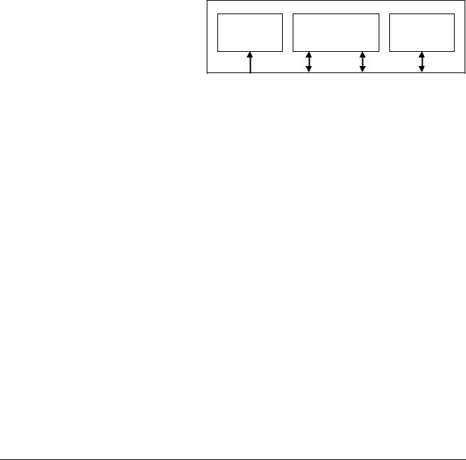
The level two memory interface exists to provide a high-bandwidth interface to second level caches, on-chip RAM, peripherals, and interfaces to external memory.
It is a key feature in ensuring high system performance, providing a higher bandwidth mechanism for filling the caches in a cache miss than has existed on previous ARM processors.
The processor level two interconnect system uses the following 64-bit wide AXI interfaces:
•Instruction Fetch Interface
•Data Read/Write Interface
•DMA Interface.
Another interface is also provided, the Peripheral Interface. This is a 32-bit AXI interface.
Figure 8-1 shows the level two interconnect interfaces.
|
|
Processor |
|
||
Level |
two |
Level |
two data side |
|
|
instruction side |
DMA |
||||
controller |
|||||
controller |
|
||||
|
|
|
|||
Instruction fetch |
Data read/write |
Peripheral |
DMA |
port |
port |
port |
port |
(64-bit) |
(64-bit) |
(32-bit) |
(64-bit) |
Figure 8-1 Level two interconnect interfaces
These interfaces provide for several simultaneous outstanding transactions, giving the potential for high performance from level two memory systems that support parallelism, and also for high utilization of pipelined memories such as SDRAM.
•No outstanding accesses are issued on the DMA port. The DMA port can issue bursts of 32-bit or 64-bit data when the address is correctly aligned.
•The data read/write port can issue outstanding accesses. The maximum number of outstanding accesses it can issue is two reads and two writes, to give a total of four outstanding accesses.
•The instruction port can issue outstanding read accesses, up to a maximum of two outstanding read accesses.
•No outstanding accesses are issued by the peripheral port.
Each of the four wide interfaces is an AXI interface, with additional signals to support additional features for the level two memory system for multi-level cache support.
The processor does not drive the following AXI ID signals:
•ARIDI
•ARIDRW
•AWIDRW
•WIDRW
•ARIDP
•AWIDP
•WIDP
•ARIDD
ARM DDI 0333H |
Copyright © 2004-2009 ARM Limited. All rights reserved. |
8-2 |
ID012410 |
Non-Confidential, Unrestricted Access |
|

Level Two Interface
•AWIDD
•WIDD.
When you connect the processor in an AXI system, you can choose whatever ID value suits your system. The only requirement is that AWID and WID must have the same value.
8.1.1AXI parameters for the level 2 interconnect interfaces
Table 8-1 shows the AXI parameters for the level 2 interconnect interfaces.
Table 8-1 AXI parameters for the level 2 interconnect interfaces
Parameter |
Interface: |
|
|
|
|
Instruction, RO |
Data, RW |
Peripheral, RW |
DMA, RW |
||
|
|||||
|
|
|
|
|
|
Write Issuing Capability |
Not applicable |
2 |
1 |
1 |
|
|
|
|
|
|
|
Read Issuing Capability |
2 |
2 |
1 |
1 |
|
|
|
|
|
|
|
Combined Issuing Capability |
Not applicable |
4 |
1 |
1 |
|
|
|
|
|
|
|
Write ID Capability |
Not applicable |
1 |
1 |
1 |
|
|
|
|
|
|
|
Write Interleave Capability |
Not applicable |
1a |
1a |
1a |
|
Write ID Width |
Not applicableb |
Not applicableb |
Not applicableb |
Not applicableb |
|
Read ID Capability |
1 |
1 |
1 |
1 |
|
|
|
|
|
|
|
Read ID Width |
Not applicableb |
Not applicableb |
Not applicableb |
Not applicableb |
a.The value of 1 means that interleaving or re-ordering cannot occur.
b.The level 2 interconnect interfaces do not implement any AXI ID signals.
8.1.2Level two instruction-side controller
The level two instruction-side controller contains the level two Instruction Fetch Interface. See
Instruction Fetch Interface.
The level two instruction-side controller handles all instruction-side cache misses including those for Noncacheable locations. It is responsible for the sequencing of cache operations for Instruction Cache linefills, making requests for the individual stores through the Prefetch Unit (PU) to the Instruction Cache. The decoupling involved means that the level two instruction-side controller contains some buffering.
Instruction Fetch Interface
The Instruction Fetch Interface is a read-only interface that services the Instruction Cache on cache misses, including the fetching of instructions for the PU that are held in memory marked as Noncacheable. The interface is optimized for cache linefills rather than individual requests.
8.1.3Level two data-side controller
The level two data-side controller is responsible for the level two:
•Data Read/Write Interface
•Peripheral Interface.
ARM DDI 0333H |
Copyright © 2004-2009 ARM Limited. All rights reserved. |
8-3 |
ID012410 |
Non-Confidential, Unrestricted Access |
|

Level Two Interface
The level two data-side controller handles:
•All external access requests from the Load Store Unit, including cache misses, data Write-Through operations, and Noncacheable data.
•SWP instructions and semaphore operations. It schedules all reads and writes on the two interfaces, that are closely related.
The level two data-side controller also handles the Peripheral Interface.
The level two data-side controller contains the Refill and Write-Back engines for the Data Cache. These make requests through the Load Store Unit for the individual cache operations that are required. The decoupling involved means that the level two data-side controller contains some buffering. The write buffer is an integral part of the level two data-side controller.
Data Read/Write Interface
The Data Read/Write Interface performs reads and swap reads. It services the Data Cache on cache misses, and reads noncacheable locations.
The Data Read/Write Interface performs writes and swap writes. It services the writes out of the Write Buffer. Multiple writes can be queued up as part of this interface.
Peripheral Interface
The Peripheral Interface is a bidirectional AXI interface that services peripheral devices. In ARM1176JZ-S processors, the Peripheral Interface is used for peripherals that are private to the processor, such as the Vectored Interrupt Controller or Watchdog Timer. Accesses to regions of memory that are marked as Device and Non-Shared are routed to the Peripheral Interface in preference to the Data Read/Write Interface.
Instruction and DMA accesses are not routed to the Peripheral port.
Unaligned accesses and exclusive accesses are not supported by the peripheral port, because they are not supported in Device memory. The order that accesses are presented on the Peripheral Interface, relative to those on the Data Read/Write Interface is not defined, other than Strongly Ordered accesses. For this reason, the peripheral port is expected to be used to access a bus or memory system that is not accessible through the Data Read/Write port. See c15, Peripheral Port Memory Remap Register on page 3-130 to find out how to remap data accesses to a defined address region to the peripheral port. In some systems, designers might not want to use the Peripheral port to access locations in memory that are marked in the page tables as Non-Shared Device. In these cases, you can use the Remap Registers to remap Non-Shared Device to Shared Device, so causing these accesses to be made using the main system memory ports.
8.1.4DMA
The DMA is responsible for:
•Performing all external memory transactions required by the DMA engine, and for requesting accesses from the Instruction TCM and Data TCM as required.
•Queuing the DMA channels as required. The DMA Interface contains several registers that are CP15 registers dedicated for DMA use, see DMA control on page 3-9 for details.
The DMA contains buffering to enable the decoupling of internal and external requests. This is because of variable latency between internal and external accesses.
ARM DDI 0333H |
Copyright © 2004-2009 ARM Limited. All rights reserved. |
8-4 |
ID012410 |
Non-Confidential, Unrestricted Access |
|

Level Two Interface
It uses the Prefetch Unit (PU) and the Load Store Unit (LSU) to schedule its accesses to the TCMs.
DMA Interface
The DMA Interface is a bidirectional interface that services the DMA subsystem for writing and reading the TCMs. Although the DMA Interface is bidirectional, it is able to produce a stream of successive accesses that are in the same direction, followed by either an extra stream in the same direction, or a stream in the opposite direction. Correspondingly the direction turnaround is not significantly optimized.
The size of the transfer is given in the parameters of the transfer in the CP15 registers. The transfers are always aligned with the size of the transfer as indicated by the CP15 registers.
ARM DDI 0333H |
Copyright © 2004-2009 ARM Limited. All rights reserved. |
8-5 |
ID012410 |
Non-Confidential, Unrestricted Access |
|