


Chapter 2
Programmer’s Model
This chapter describes the processor registers and provides information for programming the microprocessor. It contains the following sections:
•About the programmer’s model on page 2-2
•Secure world and Non-secure world operation with TrustZone on page 2-3
•Processor operating states on page 2-12
•Instruction length on page 2-13
•Data types on page 2-14
•Memory formats on page 2-15
•Addresses in a processor system on page 2-16
•Operating modes on page 2-17
•Registers on page 2-18
•The program status registers on page 2-24
•Additional instructions on page 2-30
•Exceptions on page 2-36
•Software considerations on page 2-59.
ARM DDI 0333H |
Copyright © 2004-2009 ARM Limited. All rights reserved. |
2-1 |
ID012410 |
Non-Confidential, Unrestricted Access |
|
Programmer’s Model
2.1About the programmer’s model
The processors implement ARM architecture v6 with Java extensions and TrustZone™ security extensions.
The architecture includes the 32-bit ARM instruction set, 16-bit Thumb instruction set, and the 8-bit Java instruction set. For details of both the ARM and Thumb instruction sets, see the ARM Architecture Reference Manual. For the Java instruction set see the Jazelle V1 Architecture Reference Manual.
TrustZone provides Secure and Non-secure worlds for software to operate in. For more details see Secure world and Non-secure world operation with TrustZone on page 2-3 and the ARM Architecture Reference Manual.
ARM DDI 0333H |
Copyright © 2004-2009 ARM Limited. All rights reserved. |
2-2 |
ID012410 |
Non-Confidential, Unrestricted Access |
|
Programmer’s Model
2.2Secure world and Non-secure world operation with TrustZone
This section describes;
•TrustZone model
•How the Secure model works on page 2-4.
For more details on TrustZone and the ARM architecture, see the ARM Architecture Reference Manual.
2.2.1TrustZone model
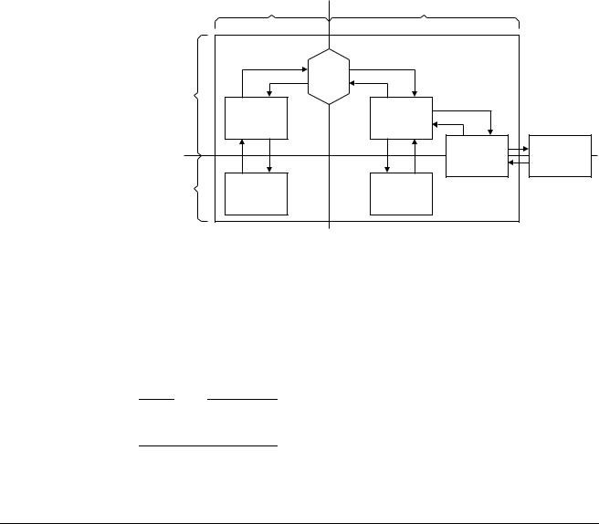
The basis of the TrustZone model is that the computing environment splits into two isolated worlds, the Secure world and the Non-secure world, with no leakage of Secure data to the Non-secure world. Software Secure Monitor code, running in the Secure Monitor Mode, links the two worlds and acts as a gatekeeper to manage program flow. The system can have both Secure and Non-secure peripherals that suitable Secure and Non-secure device drivers control. Figure 2-1 shows the relationship between the Secure and Non-secure worlds. The Operating System (OS) splits into the Secure OS, that includes the Secure kernel, and the Non-secure OS, that includes the Non-secure kernel. For details on modes of operation, see Operating modes on page 2-17.
Non-secure |
Secure |
|
Fixed entry |
Fixed entry |
|
modes |
points |
points |
|
|
Monitor |
|
|
|
|
|
|
Privileged |
Non-secure |
Secure |
|
kernel |
kernel |
|
|
|
|
|
|
|
|
Secure |
Secure |
mode |
|
device driver |
device |
Non-secure |
Secure |
|
|
User |
|
||
application |
tasks |
|
|
|
|
|
Figure 2-1 Secure and Non-secure worlds
In normal Non-secure operation the OS runs tasks in the usual way. When a User process requires Secure execution it makes a request to the Non-secure kernel, that operates in privileged mode, and this calls the Secure Monitor to transfer execution to the Secure world.
This approach to secure systems means that the platform OS, that works in the Non-secure world, has only a few fixed entry points into the Secure world through the Secure Monitor. The trusted code base for the Secure world, that includes the Secure kernel and Secure device drivers, is small and therefore much easier to maintain and verify.
Note
Software that runs in User mode cannot directly switch the world that it operates in. Changes from one world to the other can only occur through the Secure Monitor mode.
ARM DDI 0333H |
Copyright © 2004-2009 ARM Limited. All rights reserved. |
2-3 |
ID012410 |
Non-Confidential, Unrestricted Access |
|

Programmer’s Model
2.2.2How the Secure model works
This section describes how the Secure model works from a program perspective and includes:
•The NS bit and Secure Monitor mode
•Secure memory management on page 2-5
•System boot sequence on page 2-8
•Secure interrupts on page 2-8
•Secure peripherals on page 2-8
•Secure debug on page 2-9.
The NS bit and Secure Monitor mode
The Non-secure (NS) bit determines if the program execution is in the Secure or Non-secure world. The NS bit is in the Secure Configuration Register (SCR) in coprocessor CP15, see c1, Secure Configuration Register on page 3-52. All the modes of the core, except the Secure Monitor, can operate in either the Secure or Non-secure worlds, so there are both Secure and Non-secure User modes and Secure and Non-secure privileged modes, see Operating modes on page 2-17 and Registers on page 2-18.
Note
An attempt to access the SCR directly in User modes, Secure or Non-secure, or in Non-secure privileged modes, makes the processor enter the Undefined exception trap. SCR can only be accessed in Secure privileged modes.
Secure Monitor mode is a privileged mode and is always Secure regardless of the state of the NS bit. The Secure Monitor is code that runs in Secure Monitor mode and processes switches to and from the Secure world. The overall security of the software relies on the security of this code along with the Secure boot code.
When the Secure Monitor transfers control from one world to the other it must save the processor context, that includes register banks, from one world and restore those for the other world. The processor hardware automatically shadows and changes context information in CP15 registers appropriately.
If the Secure Monitor determines that a change from one world to the other is valid it writes to the NS bit to change the world in operation. Although all Secure privileged modes can access the NS bit, it is strongly recommended that you only use the Secure Monitor to change the NS bit. See the ARM Architecture Reference Manual for more information.
A Secure Monitor Call (SMC) is used to enter the Secure Monitor mode and perform a Secure Monitor kernel service call. This instruction can only be executed in privileged modes, so when a User process wants to request a change from one world to the other it must first execute a SVC instruction. This changes the processor to a privileged mode where the Supervisor call handler processes the SVC and executes a SMC, see Exceptions on page 2-36.
Note
An attempt by a User process to execute an SMC makes the processor enter the Undefined exception trap.
The Secure Monitor mode is responsible for the switch from one world to the other. You must only modify the SCR in Secure Monitor mode.
The recommended way to return to the Non-secure world is to:
1.Set the NS bit in the SCR.
ARM DDI 0333H |
Copyright © 2004-2009 ARM Limited. All rights reserved. |
2-4 |
ID012410 |
Non-Confidential, Unrestricted Access |
|

Programmer’s Model
2.Execute a MOVS, SUBS or RFE.
All ARM implementations ensure that the processor can not execute the prefetched instructions that follow MOVS, SUBS, or equivalents, with Secure access permissions.
It is strongly recommended that you do not use an MSR instruction to switch from the Secure to the Non-secure world. There is no guarantee that, after the NS bit is set in Secure Monitor mode, an MSR instruction avoids execution of prefetched instructions with Secure access permission. This is because the processor prefetches the instructions that follow the MSR with Secure privileged permissions and this might form a security hole in the system if the prefetched instructions then execute in the Non-secure world.
If the prefetched instructions are in Non-secure memory, with the MSR at the boundary between Secure and Non-secure memory, they might be corrupted to give Secure information to the Non-secure world.
To avoid this problem with the MSR instruction, you can use an IMB sequence shortly after the MSR. If you use the IMB sequence you must ensure that the instructions that execute after the MSR and before the IMB do not leak any information to the Non-secure world and do not rely on the Secure permission level.
It is strongly recommended that you do not set the NS bit in Privileged modes other than in Secure Monitor mode. If you do so you face the same problem as a return to the Non-secure world with the MSR instruction.
Note
To avoid leakage after an MSR instruction use an IMB sequence.
To enter the Secure Monitor the processor executes:
SMC {<cond>} <imm16>
Where:
<cond> Is the condition when the processor executes the SMC
<imm16> The processor ignores this 16-bit immediate value, but the Secure Monitor can use it to determine the service to provide.
To return from the Secure Monitor the processor executes:
MOVS PC, R14_mon
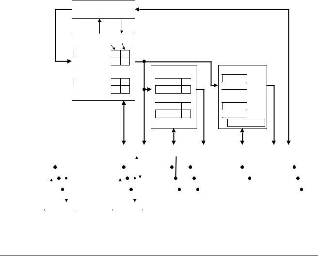
Secure memory management
The principle of TrustZone memory management is to partition the physical memory into Secure and Non-secure regions. The Secure protection is ensured by checking all physical access to memory or peripherals. There are various means to split the global physical memory into Secure and Non-secure regions. This can be done at each slave level, in the memory controller, or in a global module, for example. The partition can be hard-wired or configurable. All systems can have specific requirements, but the partitioning must be done so that any
Non-secure access to Secure memory or device causes an external abort to the core, a security violation. An AXI signal AxPROT[1] indicates whether the current access is Secure or not and
is used to check the access.
The Secure information exists at any stage of the memory management to guarantee the integrity of data:
•at L2 stage, you can split the memory mapping into Secure and Non-secure regions
ARM DDI 0333H |
Copyright © 2004-2009 ARM Limited. All rights reserved. |
2-5 |
ID012410 |
Non-Confidential, Unrestricted Access |
|
Programmer’s Model
•in the MMU, Secure and Non-secure descriptors can coexist and they are differentiated by the NSTID.
In the descriptors the NS attribute indicates whether the corresponding physical memory is Secure or Non-secure.
For Non-secure descriptors, marked with NSTID=Non-secure, NS attribute is forced to Non-secure value. The Non-secure world can only target Non-secure memory.
For Secure descriptor, marked with NSTID=Secure, NS attribute indicates if the physical memory targets Secure or Non-secure memory:
In the caches, instruction and data, each line is tagged as Secure or Non-secure, so that Secure and Non-secure data can coexist in the cache. Each time a cache line fill is performed, the NS tag is updated appropriately.
For external accesses, AxPROT[1] indicates whether the access is Secure or Non-secure.
The TrustZone security extensions are completely compatible with existing software. This means that existing applications and operating systems access memory without change. Where a system employs Secure functionality the Non-secure world is effectively blind to Secure memory. This means that Secure and Non-secure memory can co-exist with no affect on Non-secure code.
Figure 2-2 shows the basic connection of the Secure and Non-secure memory.
Core
Data
Abort
Core world state
Address |
MMU |
NSTID |
|
||
|
NS attribute |
|
Descriptor 1 |
S |
S |
|
|
|
|
Descriptor 2 |
NS NS |
|
|
|
||
|
|
|
Cache |
|
TCM |
|
Descriptor (n-1) NS NS |
Line 1 |
S |
Line 1 |
|||
Line 2 |
||||||
Descriptor (n) |
NS |
S |
Line 2 |
NS |
||
|
||||||
|
|
|
Line(n-1) |
NS |
Line(n-1) |
|
|
Page |
|
Line (n) |
S |
Line(n) |
|
|
|
|
|
|
||
|
table |
|
|
|
NS access bit |
|
|
walk |
|
|
|
|
|
|
|
|
Data |
Data |
||
|
|
|
|
|
|
|
|
|
|
|
|
|
|
|
|
|
|
|
AXI interface |
|
|
|
|
|
|
|
|
|
|
|
|
||||||
|
|
|
|
|
|
|
|
|
|
|
|
|
|
|
|
|
|
|
|
|
|
|
|
|
|
|
|
|
|
|
|
|
|
|
|
|
|
|
|
|
|
|
|
|
|
Address |
|
Abort |
|
|
AxPROT[1] |
|
|
|
|
|
|
|
|
|
|
|
|
|
|
||||||||||
|
|
|
|
|
|
|
|
|
|
|
|
|
|
|
|
|
|
|
|
|
|
|
|
|
|
|
|||||||||||
|
|
|
|
|
|
|
|
|
|
|
|
|
|
|
|
|
|
|
|
|
|
|
|
|
|
|
|
|
|
|
|
|
|
|
|
||
|
|
|
|
|
|
|
|
|
|
|
|
|
|
|
|
|
|
|
|
|
|
|
|
|
|
|
|
|
|
|
|
|
|
|
|
|
|
|
|
|
|
|
|
|
|
Control |
|
|
|
|
|
|
|
|
|
|
|
|
|
|
|
|
|
|
|
|
|
|
|
|
|
|
|
|
|
|
|
|
|
|
|
|
|
|
|
|
|
|
|
|
|
|
|
|
|
|
|
|
|
|
|
|
|
|
|
|
|
|
|
|
|
||
|
|
|
|
|
|
|
|
|
|
|
|
|
|
|
|
|
|
|
|
|
|
|
|
|
|
|
|
|
|
|
|
|
|
|
|
||
|
|
|
|
|
|
|
|
Data |
|
|
|
|
|
|
|
|
|
|
|
|
|
|
|
|
|
|
|
|
|
|
|
|
|
|
|
|
|
|
|
|
|
|
|
|
|
|
|
|
|
|
|
|
|
|
|
|
|
|
|
|
|
|
|
|
|
|
|
|
|
|
|
|
|
||
|
|
|
|
|
|
|
|
|
|
|
|
|
|
|
|
|
|
|
|
|
|
|
|
|
|
|
|
|
|
|
|
|
|
|
|
|
|
Abort |
|
|
|
|
|
AxPROT[1] Abort |
|
|
|
|
|
|
|
AxPROT[1] |
|
|
|
|
|
|
|
|
|
|
|
|
|
|
|
||||||||
|
|
|
|
|
|
|
|
|
|
|
|
|
|
|
|
|
|
|
|
|
|
|
|
|
|
|
|||||||||||
|
|
|
|
|
|
|
|
|
|
|
|
|
|
|
|
|
|
|
|
|
|
|
|
|
|
|
|||||||||||
|
|
|
S prot |
|
|
|
S prot |
|
|
|
|
|
Non- |
|
|
|
|
|
|
|
|
|
|
|
|
|
|||||||||||
|
|
|
|
|
|
|
|
|
|
|
|
|
|
|
|
|
|
|
|
|
|
|
|
|
|
|
|
|
Master |
|
|||||||
|
|
External |
|
|
Secure |
|
|
|
|
|
secure |
|
|
Arbiter |
Decoder |
|
|
|
|||||||||||||||||||
|
|
|
|
|
|
|
|
|
|
|
|
|
peripheral |
|
|||||||||||||||||||||||
|
|
memory |
|
|
|
slave |
|
|
|
|
|
slave |
|
|
|
|
|
|
|
|
|
||||||||||||||||
|
|
|
|
|
|
|
|
|
|
|
|
|
|
|
|
|
|
|
|
|
|
|
|||||||||||||||
|
|
|
|
|
|
|
|
|
|
|
|
|
|
|
|
|
|
|
|
|
|
|
|
|
|
|
|
|
|
|
|
|
|
|
|
|
|
Figure 2-2 Memory in the Secure and Non-secure worlds
ARM DDI 0333H |
Copyright © 2004-2009 ARM Limited. All rights reserved. |
2-6 |
ID012410 |
Non-Confidential, Unrestricted Access |
|
Programmer’s Model
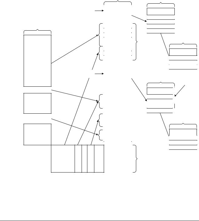
The virtual memory address map for the Secure and Non-secure worlds appear as separate blocks. Figure 2-3 shows how the Secure and Non-secure virtual address spaces might map onto the physical address space. In this example:
•Non-secure descriptors are stored in Non-secure memory and can only target Non-secure memory
•Secure descriptors are stored in Secure memory and can target both Secure and Non-secure memory.
Non-secure Virtual memory
Non-secure translation table base address
Secure translation table base address
Physical memory
|
|
|
Non-secure level |
|
|
1 descriptors |
|
|
|
|
|
|
|
|
4KB non-secure |
RAM |
|
4KB non-secure |
||
|
||
4KB non-secure |
chip- |
|
4KB non-secure |
||
|
||
4KB non-secure |
on |
|
4KB secure |
32KB |
|
4KB secure |
||
4KB secure |
|
|
|
|
|
Secure level 1 |
|
|
descriptors |
|
|
|
|
|
Non-secure |
|
|
SDRAM |
|
|
|
|
|
|
|
|
Secure |
|
|
peripherals |
|
|
|
|
|
|
|
|
Non-secure |
|
|
peripherals |
|
|
|
Secure Virtual memory |
|
|
Non-secure level 1 descriptors
1MB sections
Non-secure level 2 descriptors
 4KB small pages
Secure level 1
descriptors NS attribute
1MB sections
Secure level 2 descriptors
 4KB small pages
Figure 2-3 Memory partition in the Secure and Non-secure worlds
ARM DDI 0333H |
Copyright © 2004-2009 ARM Limited. All rights reserved. |
2-7 |
ID012410 |
Non-Confidential, Unrestricted Access |
|

Programmer’s Model
System boot sequence
Caution
TrustZone security extensions enable a Secure software environment. The technology does not protect the processor from hardware attacks and the implementor must make sure that the hardware that contains the boot code is appropriately secure.
The processor always boots in the privileged Supervisor mode in the Secure world, that is the NS bit is 0. This means that code not written for TrustZone always runs in the Secure world, but has no way to switch to the Non-secure world. Because the Secure and Non-secure worlds mirror each other this Secure operation does not affect the functionality of code not written for TrustZone. The processor is therefore compatible with other ARMv6 architectures. Peripherals boot in their most Secure state.
The Secure OS code at the reset vector must:
1.Initialize the Secure OS. This includes normal boot actions such as:
a.Generate page tables and switch on the MMU if the design uses caches or memory protection.
b.Switch on the stack.
c.Set up the run time environment and program stacks for each processor mode.
2.Initialize the Secure Monitor. This includes such actions as:
a.Allocate TCM memory for the Secure Monitor code.
b.Allocate scratch work space.
c.Set up the Secure Monitor stack pointer and initialize its state block.
3.Program the partition checker to allocate physical memory available to the Non-secure OS.
4.Yield control to the Non-secure OS. The Non-secure OS boots after this.
The overall security of the software relies on the security of the boot code along with the code for the Secure Monitor.
Secure interrupts
There are no new pins to deal with Secure interrupts. However the IRQ and FIQ bits in the SCR can be set to 1, so that the core branches to Secure Monitor mode, instead of IRQ or FIQ mode, when an interrupt occurs. For more information see c1, Secure Configuration Register on page 3-52.
FIQ can be used to enter the Secure world in a deterministic way, if it is configured as NMI when the core is in the Non-secure world,. This configuration is done using the FW and FIQ bits in SCR. The nIRQ pin can also be used as Secure interrupt and can enter directly monitor mode, if the IRQ bit in the SCR is set to 1. But it might be masked in the Non-secure world if the I bit in the CPSR is set to 1.
Secure peripherals
You can protect a Secure peripheral by mapping it to a Secure memory region. In addition, you can protect Secure peripherals by checking the AxPROT[1] signal and generating an error
response if a Non-secure access attempts to read or write a Secure register.
ARM DDI 0333H |
Copyright © 2004-2009 ARM Limited. All rights reserved. |
2-8 |
ID012410 |
Non-Confidential, Unrestricted Access |
|