

- •Contents
- •List of Tables
- •List of Figures
- •Preface
- •About this manual
- •Product revision status
- •Intended audience
- •Using this manual
- •Conventions
- •Additional reading
- •Feedback
- •Feedback on the product
- •Feedback on this book
- •Introduction
- •1.1 About the processor
- •1.2 Extensions to ARMv6
- •1.3 TrustZone security extensions
- •1.4.1 Instruction compression
- •1.4.2 The Thumb instruction set
- •1.4.3 Java bytecodes
- •1.5 Components of the processor
- •1.5.1 Integer core
- •1.5.2 Load Store Unit (LSU)
- •1.5.3 Prefetch unit
- •1.5.4 Memory system
- •1.5.5 AMBA AXI interface
- •1.5.6 Coprocessor interface
- •1.5.7 Debug
- •1.5.8 Instruction cycle summary and interlocks
- •1.5.9 System control
- •1.5.10 Interrupt handling
- •1.6 Power management
- •1.7 Configurable options
- •1.8 Pipeline stages
- •1.9 Typical pipeline operations
- •1.9.1 Instruction progression
- •1.10.1 Extended ARM instruction set summary
- •1.10.2 Thumb instruction set summary
- •1.11 Product revisions
- •Programmer’s Model
- •2.1 About the programmer’s model
- •2.2.1 TrustZone model
- •2.2.2 How the Secure model works
- •2.2.3 TrustZone write access disable
- •2.2.4 Secure Monitor bus
- •2.3 Processor operating states
- •2.3.1 Switching state
- •2.3.2 Interworking ARM and Thumb state
- •2.4 Instruction length
- •2.5 Data types
- •2.6 Memory formats
- •2.7 Addresses in a processor system
- •2.8 Operating modes
- •2.9 Registers
- •2.9.1 The ARM state core register set
- •2.9.2 The Thumb state core register set
- •2.9.3 Accessing high registers in Thumb state
- •2.9.4 ARM state and Thumb state registers relationship
- •2.10 The program status registers
- •2.10.1 The condition code flags
- •2.10.2 The Q flag
- •2.10.4 The GE[3:0] bits
- •2.10.7 The control bits
- •2.10.8 Modification of PSR bits by MSR instructions
- •2.10.9 Reserved bits
- •2.11 Additional instructions
- •2.11.1 Load or Store Byte Exclusive
- •2.11.2 Load or Store Halfword Exclusive
- •2.11.3 Load or Store Doubleword
- •2.11.4 CLREX
- •2.12 Exceptions
- •2.12.1 New instructions for exception handling
- •2.12.2 Exception entry and exit summary
- •2.12.3 Entering an ARM exception
- •2.12.4 Leaving an ARM exception
- •2.12.5 Reset
- •2.12.6 Fast interrupt request
- •2.12.7 Interrupt request
- •2.12.8 Low interrupt latency configuration
- •2.12.9 Interrupt latency example
- •2.12.10 Aborts
- •2.12.11 Imprecise Data Abort mask in the CPSR/SPSR
- •2.12.12 Supervisor call instruction
- •2.12.13 Secure Monitor Call (SMC)
- •2.12.14 Undefined instruction
- •2.12.15 Breakpoint instruction (BKPT)
- •2.12.16 Exception vectors
- •2.12.17 Exception priorities
- •2.13 Software considerations
- •2.13.1 Branch Target Address Cache flush
- •2.13.2 Waiting for DMA to complete
- •System Control Coprocessor
- •3.1 About the system control coprocessor
- •3.1.1 System control coprocessor functional groups
- •3.1.2 System control and configuration
- •3.1.3 MMU control and configuration
- •3.1.4 Cache control and configuration
- •3.1.5 TCM control and configuration
- •3.1.6 Cache Master Valid Registers
- •3.1.7 DMA control
- •3.1.8 System performance monitor
- •3.1.9 System validation
- •3.1.10 Use of the system control coprocessor
- •3.2 System control processor registers
- •3.2.1 Register allocation
- •3.2.2 c0, Main ID Register
- •3.2.3 c0, Cache Type Register
- •3.2.4 c0, TCM Status Register
- •3.2.5 c0, TLB Type Register
- •3.2.6 c0, CPUID registers
- •3.2.7 c1, Control Register
- •3.2.8 c1, Auxiliary Control Register
- •3.2.9 c1, Coprocessor Access Control Register
- •3.2.10 c1, Secure Configuration Register
- •3.2.11 c1, Secure Debug Enable Register
- •3.2.13 c2, Translation Table Base Register 0
- •3.2.14 c2, Translation Table Base Register 1
- •3.2.15 c2, Translation Table Base Control Register
- •3.2.16 c3, Domain Access Control Register
- •3.2.17 c5, Data Fault Status Register
- •3.2.18 c5, Instruction Fault Status Register
- •3.2.19 c6, Fault Address Register
- •3.2.20 c6, Watchpoint Fault Address Register
- •3.2.21 c6, Instruction Fault Address Register
- •3.2.22 c7, Cache operations
- •3.2.23 c8, TLB Operations Register
- •3.2.24 c9, Data and instruction cache lockdown registers
- •3.2.25 c9, Data TCM Region Register
- •3.2.26 c9, Instruction TCM Region Register
- •3.2.29 c9, TCM Selection Register
- •3.2.30 c9, Cache Behavior Override Register
- •3.2.31 c10, TLB Lockdown Register
- •3.2.32 c10, Memory region remap registers
- •3.2.33 c11, DMA identification and status registers
- •3.2.34 c11, DMA User Accessibility Register
- •3.2.35 c11, DMA Channel Number Register
- •3.2.36 c11, DMA enable registers
- •3.2.37 c11, DMA Control Register
- •3.2.38 c11, DMA Internal Start Address Register
- •3.2.39 c11, DMA External Start Address Register
- •3.2.40 c11, DMA Internal End Address Register
- •3.2.41 c11, DMA Channel Status Register
- •3.2.42 c11, DMA Context ID Register
- •3.2.44 c12, Monitor Vector Base Address Register
- •3.2.45 c12, Interrupt Status Register
- •3.2.46 c13, FCSE PID Register
- •3.2.47 c13, Context ID Register
- •3.2.48 c13, Thread and process ID registers
- •3.2.49 c15, Peripheral Port Memory Remap Register
- •3.2.51 c15, Performance Monitor Control Register
- •3.2.52 c15, Cycle Counter Register
- •3.2.53 c15, Count Register 0
- •3.2.54 c15, Count Register 1
- •3.2.55 c15, System Validation Counter Register
- •3.2.56 c15, System Validation Operations Register
- •3.2.57 c15, System Validation Cache Size Mask Register
- •3.2.58 c15, Instruction Cache Master Valid Register
- •3.2.59 c15, Data Cache Master Valid Register
- •3.2.60 c15, TLB lockdown access registers
- •Unaligned and Mixed-endian Data Access Support
- •4.2 Unaligned access support
- •4.2.1 Legacy support
- •4.2.2 ARMv6 extensions
- •4.2.3 Legacy and ARMv6 configurations
- •4.2.4 Legacy data access in ARMv6 (U=0)
- •4.2.5 Support for unaligned data access in ARMv6 (U=1)
- •4.2.6 ARMv6 unaligned data access restrictions
- •4.3 Endian support
- •4.3.1 Load unsigned byte, endian independent
- •4.3.2 Load signed byte, endian independent
- •4.3.3 Store byte, endian independent
- •4.4 Operation of unaligned accesses
- •4.5.1 Legacy fixed instruction and data endianness
- •4.5.3 Reset values of the U, B, and EE bits
- •4.6.1 All load and store operations
- •4.7 Instructions to change the CPSR E bit
- •Program Flow Prediction
- •5.1 About program flow prediction
- •5.2 Branch prediction
- •5.2.1 Enabling program flow prediction
- •5.2.2 Dynamic branch predictor
- •5.2.3 Static branch predictor
- •5.2.4 Branch folding
- •5.2.5 Incorrect predictions and correction
- •5.3 Return stack
- •5.4 Memory Barriers
- •5.4.1 Instruction Memory Barriers (IMBs)
- •5.5.1 Execution of IMB instructions
- •Memory Management Unit
- •6.1 About the MMU
- •6.2 TLB organization
- •6.2.1 MicroTLB
- •6.2.2 Main TLB
- •6.2.3 TLB control operations
- •6.2.5 Supersections
- •6.3 Memory access sequence
- •6.3.1 TLB match process
- •6.3.2 Virtual to physical translation mapping restrictions
- •6.4 Enabling and disabling the MMU
- •6.4.1 Enabling the MMU
- •6.4.2 Disabling the MMU
- •6.4.3 Behavior with MMU disabled
- •6.5 Memory access control
- •6.5.1 Domains
- •6.5.2 Access permissions
- •6.5.3 Execute never bits in the TLB entry
- •6.6 Memory region attributes
- •6.6.1 C and B bit, and type extension field encodings
- •6.6.2 Shared
- •6.6.3 NS attribute
- •6.7 Memory attributes and types
- •6.7.1 Normal memory attribute
- •6.7.2 Device memory attribute
- •6.7.3 Strongly Ordered memory attribute
- •6.7.4 Ordering requirements for memory accesses
- •6.7.5 Explicit Memory Barriers
- •6.7.6 Backwards compatibility
- •6.8 MMU aborts
- •6.8.1 External aborts
- •6.9 MMU fault checking
- •6.9.1 Fault checking sequence
- •6.9.2 Alignment fault
- •6.9.3 Translation fault
- •6.9.4 Access bit fault
- •6.9.5 Domain fault
- •6.9.6 Permission fault
- •6.9.7 Debug event
- •6.10 Fault status and address
- •6.11 Hardware page table translation
- •6.11.2 ARMv6 page table translation subpage AP bits disabled
- •6.11.3 Restrictions on page table mappings page coloring
- •6.12 MMU descriptors
- •Level One Memory System
- •7.1 About the level one memory system
- •7.2 Cache organization
- •7.2.1 Features of the cache system
- •7.2.2 Cache functional description
- •7.2.3 Cache control operations
- •7.2.4 Cache miss handling
- •7.2.5 Cache disabled behavior
- •7.2.6 Unexpected hit behavior
- •7.3.1 TCM behavior
- •7.3.2 Restriction on page table mappings
- •7.3.3 Restriction on page table attributes
- •7.5 TCM and cache interactions
- •7.5.1 Overlapping between TCM regions
- •7.5.2 DMA and core access arbitration
- •7.5.3 Instruction accesses to TCM
- •7.5.4 Data accesses to the Instruction TCM
- •7.6 Write buffer
- •Level Two Interface
- •8.1 About the level two interface
- •8.1.1 AXI parameters for the level 2 interconnect interfaces
- •8.2 Synchronization primitives
- •8.2.3 Example of LDREX and STREX usage
- •8.3 AXI control signals in the processor
- •8.3.1 Channel definition
- •8.3.2 Signal name suffixes
- •8.3.3 Address channel signals
- •8.4 Instruction Fetch Interface transfers
- •8.4.1 Cacheable fetches
- •8.4.2 Noncacheable fetches
- •8.5 Data Read/Write Interface transfers
- •8.5.1 Linefills
- •8.5.2 Noncacheable LDRB
- •8.5.3 Noncacheable LDRH
- •8.5.4 Noncacheable LDR or LDM1
- •8.5.5 Noncacheable LDRD or LDM2
- •8.5.6 Noncacheable LDM3
- •8.5.7 Noncacheable LDM4
- •8.5.8 Noncacheable LDM5
- •8.5.9 Noncacheable LDM6
- •8.5.10 Noncacheable LDM7
- •8.5.11 Noncacheable LDM8
- •8.5.12 Noncacheable LDM9
- •8.5.13 Noncacheable LDM10
- •8.5.14 Noncacheable LDM11
- •8.5.15 Noncacheable LDM12
- •8.5.16 Noncacheable LDM13
- •8.5.17 Noncacheable LDM14
- •8.5.18 Noncacheable LDM15
- •8.5.19 Noncacheable LDM16
- •8.6 Peripheral Interface transfers
- •8.7 Endianness
- •8.8 Locked access
- •Clocking and Resets
- •9.1 About clocking and resets
- •9.2 Clocking and resets with no IEM
- •9.2.1 Processor clocking with no IEM
- •9.2.2 Reset with no IEM
- •9.3 Clocking and resets with IEM
- •9.3.1 Processor clocking with IEM
- •9.3.2 Reset with IEM
- •9.4 Reset modes
- •9.4.1 Power-on reset
- •9.4.2 CP14 debug logic
- •9.4.3 Processor reset
- •9.4.4 DBGTAP reset
- •9.4.5 Normal operation
- •Power Control
- •10.1 About power control
- •10.2 Power management
- •10.2.1 Run mode
- •10.2.2 Standby mode
- •10.2.3 Shutdown mode
- •10.2.4 Dormant mode
- •10.2.5 Communication to the Power Management Controller
- •10.3 Intelligent Energy Management
- •10.3.1 Purpose of IEM
- •10.3.2 Structure of IEM
- •10.3.3 Operation of IEM
- •Coprocessor Interface
- •11.1 About the coprocessor interface
- •11.2 Coprocessor pipeline
- •11.2.1 Coprocessor instructions
- •11.2.2 Coprocessor control
- •11.2.3 Pipeline synchronization
- •11.2.4 Pipeline control
- •11.2.5 Instruction tagging
- •11.2.6 Flush broadcast
- •11.3 Token queue management
- •11.3.1 Queue implementation
- •11.3.2 Queue modification
- •11.3.3 Queue flushing
- •11.4 Token queues
- •11.4.1 Instruction queue
- •11.4.2 Length queue
- •11.4.3 Accept queue
- •11.4.4 Cancel queue
- •11.4.5 Finish queue
- •11.5 Data transfer
- •11.5.1 Loads
- •11.5.2 Stores
- •11.6 Operations
- •11.6.1 Normal operation
- •11.6.2 Cancel operations
- •11.6.3 Bounce operations
- •11.6.4 Flush operations
- •11.6.5 Retirement operations
- •11.7 Multiple coprocessors
- •11.7.1 Interconnect considerations
- •11.7.2 Coprocessor selection
- •11.7.3 Coprocessor switching
- •Vectored Interrupt Controller Port
- •12.1 About the PL192 Vectored Interrupt Controller
- •12.2 About the processor VIC port
- •12.2.1 Synchronization of the VIC port signals
- •12.2.2 Interrupt handler exit
- •12.3 Timing of the VIC port
- •12.3.1 PL192 VIC timing
- •12.3.2 Core timing
- •12.4 Interrupt entry flowchart
- •Debug
- •13.1 Debug systems
- •13.1.1 The debug host
- •13.1.2 The protocol converter
- •13.1.3 The processor
- •13.2 About the debug unit
- •13.2.3 Secure Monitor mode and debug
- •13.2.4 Virtual addresses and debug
- •13.2.5 Programming the debug unit
- •13.3 Debug registers
- •13.3.1 Accessing debug registers
- •13.3.2 CP14 c0, Debug ID Register (DIDR)
- •13.3.3 CP14 c1, Debug Status and Control Register (DSCR)
- •13.3.4 CP14 c5, Data Transfer Registers (DTR)
- •13.3.5 CP14 c6, Watchpoint Fault Address Register (WFAR)
- •13.3.6 CP14 c7, Vector Catch Register (VCR)
- •13.3.10 CP14 c112-c113, Watchpoint Control Registers (WCR)
- •13.3.11 CP14 c10, Debug State Cache Control Register
- •13.3.12 CP14 c11, Debug State MMU Control Register
- •13.4 CP14 registers reset
- •13.5 CP14 debug instructions
- •13.5.1 Executing CP14 debug instructions
- •13.6 External debug interface
- •13.7 Changing the debug enable signals
- •13.8 Debug events
- •13.8.1 Software debug event
- •13.8.2 External debug request signal
- •13.8.3 Halt DBGTAP instruction
- •13.8.4 Behavior of the processor on debug events
- •13.8.5 Effect of a debug event on CP15 registers
- •13.9 Debug exception
- •13.10 Debug state
- •13.10.1 Behavior of the PC in Debug state
- •13.10.2 Interrupts
- •13.10.3 Exceptions
- •13.11 Debug communications channel
- •13.12 Debugging in a cached system
- •13.12.1 Data cache writes
- •13.13 Debugging in a system with TLBs
- •13.14 Monitor debug-mode debugging
- •13.14.1 Entering the debug monitor target
- •13.14.2 Setting breakpoints, watchpoints, and vector catch debug events
- •13.14.3 Setting software breakpoint debug events (BKPT)
- •13.14.4 Using the debug communications channel
- •13.15 Halting debug-mode debugging
- •13.15.1 Entering Debug state
- •13.15.2 Exiting Debug state
- •13.15.3 Programming debug events
- •13.16 External signals
- •Debug Test Access Port
- •14.1 Debug Test Access Port and Debug state
- •14.2 Synchronizing RealView ICE
- •14.3 Entering Debug state
- •14.4 Exiting Debug state
- •14.5 The DBGTAP port and debug registers
- •14.6 Debug registers
- •14.6.1 Bypass register
- •14.6.2 Device ID code register
- •14.6.3 Instruction register
- •14.6.4 Scan chain select register (SCREG)
- •14.6.5 Scan chains
- •14.6.6 Reset
- •14.7 Using the Debug Test Access Port
- •14.7.1 Entering and leaving Debug state
- •14.7.2 Executing instructions in Debug state
- •14.7.3 Using the ITRsel IR instruction
- •14.7.4 Transferring data between the host and the core
- •14.7.5 Using the debug communications channel
- •14.7.6 Target to host debug communications channel sequence
- •14.7.7 Host to target debug communications channel
- •14.7.8 Transferring data in Debug state
- •14.7.9 Example sequences
- •14.8 Debug sequences
- •14.8.1 Debug macros
- •14.8.2 General setup
- •14.8.3 Forcing the processor to halt
- •14.8.4 Entering Debug state
- •14.8.5 Leaving Debug state
- •14.8.8 Reading the CPSR/SPSR
- •14.8.9 Writing the CPSR/SPSR
- •14.8.10 Reading the PC
- •14.8.11 Writing the PC
- •14.8.12 General notes about reading and writing memory
- •14.8.13 Reading memory as words
- •14.8.14 Writing memory as words
- •14.8.15 Reading memory as halfwords or bytes
- •14.8.16 Writing memory as halfwords/bytes
- •14.8.17 Coprocessor register reads and writes
- •14.8.18 Reading coprocessor registers
- •14.8.19 Writing coprocessor registers
- •14.9 Programming debug events
- •14.9.1 Reading registers using scan chain 7
- •14.9.2 Writing registers using scan chain 7
- •14.9.3 Setting breakpoints, watchpoints and vector traps
- •14.9.4 Setting software breakpoints
- •14.10 Monitor debug-mode debugging
- •14.10.1 Receiving data from the core
- •14.10.2 Sending data to the core
- •Trace Interface Port
- •15.1 About the ETM interface
- •15.1.1 Instruction interface
- •15.1.2 Secure control bus
- •15.1.3 Data address interface
- •15.1.4 Data value interface
- •15.1.5 Pipeline advance interface
- •15.1.6 Coprocessor interface
- •15.1.7 Other connections to the core
- •Cycle Timings and Interlock Behavior
- •16.1 About cycle timings and interlock behavior
- •16.1.1 Changes in instruction flow overview
- •16.1.2 Instruction execution overview
- •16.1.3 Conditional instructions
- •16.1.4 Opposite condition code checks
- •16.1.5 Definition of terms
- •16.2 Register interlock examples
- •16.3 Data processing instructions
- •16.3.1 Cycle counts if destination is not PC
- •16.3.2 Cycle counts if destination is the PC
- •16.3.3 Example interlocks
- •16.4 QADD, QDADD, QSUB, and QDSUB instructions
- •16.6 ARMv6 Sum of Absolute Differences (SAD)
- •16.6.1 Example interlocks
- •16.7 Multiplies
- •16.8 Branches
- •16.9 Processor state updating instructions
- •16.10 Single load and store instructions
- •16.10.1 Base register update
- •16.11 Load and Store Double instructions
- •16.12 Load and Store Multiple Instructions
- •16.12.1 Load and Store Multiples, other than load multiples including the PC
- •16.12.2 Load Multiples, where the PC is in the register list
- •16.12.3 Example Interlocks
- •16.13 RFE and SRS instructions
- •16.14 Synchronization instructions
- •16.15 Coprocessor instructions
- •16.16 SVC, SMC, BKPT, Undefined, and Prefetch Aborted instructions
- •16.17 No operation
- •16.18 Thumb instructions
- •AC Characteristics
- •17.1 Processor timing diagrams
- •17.2 Processor timing parameters
- •Signal Descriptions
- •A.1 Global signals
- •A.2 Static configuration signals
- •A.3 TrustZone internal signals
- •A.4 Interrupt signals, including VIC interface
- •A.5 AXI interface signals
- •A.5.1 Instruction read port signals
- •A.5.2 Data port signals
- •A.5.3 Peripheral port signals
- •A.5.4 DMA port signals
- •A.6 Coprocessor interface signals
- •A.7 Debug interface signals, including JTAG
- •A.8 ETM interface signals
- •A.9 Test signals
- •B.1 About the differences between the ARM1136J-S and ARM1176JZ-S processors
- •B.2 Summary of differences
- •B.2.1 TrustZone
- •B.2.2 ARMv6k extensions support
- •B.2.3 Power management
- •B.2.4 SmartCache
- •B.2.7 Tightly-Coupled Memories
- •B.2.8 Fault Address Register
- •B.2.9 Fault Status Register
- •B.2.10 Prefetch Unit
- •B.2.11 System control coprocessor operations
- •B.2.13 Debug
- •B.2.14 Level two interface
- •B.2.15 Memory BIST
- •Revisions
- •Glossary

Debug Test Access Port
14.6Debug registers
You can connect the following debug registers between DBGTDI and DBGTDO:
•Bypass register
•Device ID code register
•Instruction register on page 14-9
•Scan chain select register (SCREG) on page 14-9
•Scan chain 0, debug ID register (DIDR) on page 14-11
•Scan chain 1, Debug Status and Control Register (DSCR) on page 14-11
•Scan chain 4, instruction transfer register (ITR) on page 14-13
•Scan chain 5 on page 14-15.
•Scan chain 6 on page 14-17.
•Scan chain 7 on page 14-17.
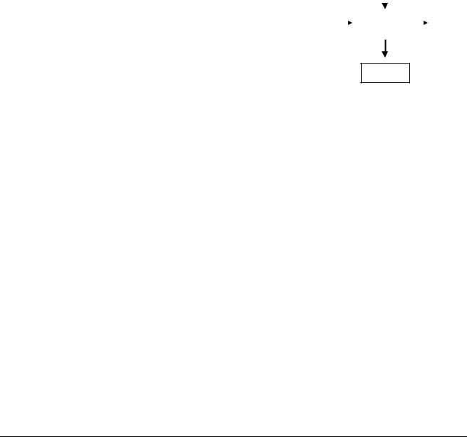
14.6.1Bypass register
Purpose |
Bypasses the device by providing a path between DBGTDI and |
|
DBGTDO. |
Length |
1 bit. |
Operating mode |
When the bypass instruction is the current instruction in the instruction |
|
register, serial data is transferred from DBGTDI to DBGTDO in the |
|
Shift-DR state with a delay of one TCK cycle. There is no parallel output |
|
from the bypass register. A logic 0 is loaded from the parallel input of the |
|
bypass register in the Capture-DR state. Nothing happens at the |
|
Update-DR state. |
Order |
Figure 14-3 shows the order of bits in the bypass register. |
|
0b0 |
DBGTDI |
|
|
Bypass |
|
|
DBGTDO |
|
|
|||||
|
|
|
|
|
|
|
Figure 14-3 Bypass register bit order
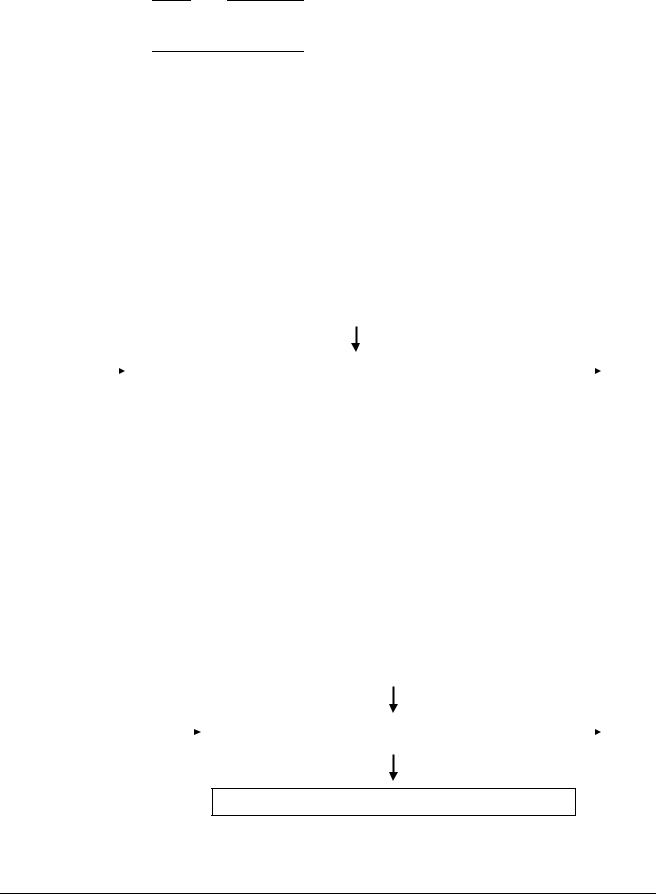
14.6.2Device ID code register
Purpose |
Device identification. To distinguish the ARM1176JZ-S processors from |
|
other processors, the DBGTAP controller ID is unique for each. This |
|
means that a DBGTAP debugger, such as RealView ICE, can easily see the |
|
processor that it is connected to. The Device ID register version and |
|
manufacturer ID fields are routed to the edge of the chip so that partners |
|
can create their own Device ID numbers by tying the pins to HIGH or |
|
LOW values. |
|
The default manufacturer ID for the ARM1176JZ-S processor is |
|
b11110000111. The part number field is hard-wired inside the |
|
ARM1176JZ-S to 0x7B76. |
ARM DDI 0333H |
Copyright © 2004-2009 ARM Limited. All rights reserved. |
14-8 |
ID012410 |
Non-Confidential, Unrestricted Access |
|

Debug Test Access Port
|
All ARM semiconductor partner-specific devices must be identified by |
|
manufacturer ID numbers of the form shown in c0, Main ID Register on |
|
page 3-20. |
Length |
32 bits. |
Operating mode When the ID code instruction is current, the shift section of the device ID register is selected as the serial path between DBGTDI and DBGTDO.
There is no parallel output from the ID register. The 32-bit device ID code is loaded into this shift section during the Capture-DR state. This is shifted out during Shift-DR, least significant bit first, while a don’t care value is shifted in. The shifted-in data is ignored in the Update-DR state.
Order |
|
Figure 14-4 shows the order of bits in the ID code register. |
|||||
31 |
28 27 |
12 11 |
1 |
0 |
|||
|
Version |
Part number |
|
Manufacturer ID |
|
1 |
|
|
|
|
|
|
|
|
|
DBGTDI |
|
|
Data[31:0] |
|
|
DBGTDO |
|
|
|||||
|
|
|
|
|
|
|
Figure 14-4 Device ID code register bit order
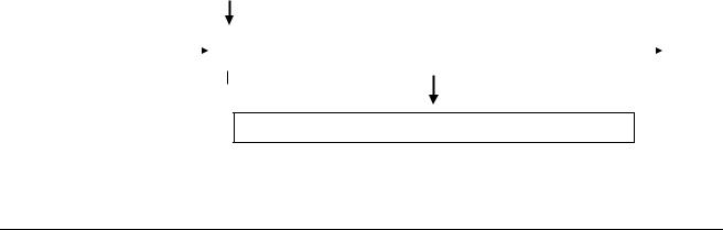
14.6.3 Instruction register |
|
|
|
|
|
|
|
|
Purpose |
Holds the current DBGTAP controller instruction. |
|
||||||
Length |
5 bits. |
|
|
|
|
|
|
|
Operating mode |
When in Shift-IR state, the shift section of the instruction register is |
|||||||
|
selected as the serial path between DBGTDI and DBGTDO. At the |
|||||||
|
Capture-IR state, the binary value b00001 is loaded into this shift section. |
|||||||
|
This is shifted out during Shift-IR, least significant bit first, while a new |
|||||||
|
instruction is shifted in, least significant bit first. At the Update-IR state, |
|||||||
|
the value in the shift section is loaded into the instruction register so it |
|||||||
|
becomes the current instruction. On DBGTAP reset, the IDcode becomes |
|||||||
|
the current instruction. |
|
|
|
|
|
|
|
Order |
Figure 14-5 shows the order of bits in the instruction register. |
|
||||||
|
|
|
|
0b00001 |
|
|||
|
DBGTDI |
|
|
|
|
|
DBGTDO |
|
|
|
|
|
|
|
|
||
|
|
|
|
|
|
|||
|
|
|
Data[4:0] |
|
|
|||
|
|
|
||||||
|
|
|
|
|
|
|
|
|
IR[4:0]
Figure 14-5 Instruction register bit order
14.6.4Scan chain select register (SCREG)
Purpose |
Holds the currently active scan chain number. |
ARM DDI 0333H |
Copyright © 2004-2009 ARM Limited. All rights reserved. |
14-9 |
ID012410 |
Non-Confidential, Unrestricted Access |
|
Debug Test Access Port
Length |
5 bits. |
Operating mode After Scan_N has been selected as the current instruction, when in
Shift-DR state, the shift section of the scan chain select register is selected as the serial path between DBGTDI and DBGTDO. At the Capture-DR
state, the binary value b10000 is loaded into this shift section. This is shifted out during Shift-DR, least significant bit first, while a new value is shifted in, least significant bit first. At the Update-DR state, the value in the shift section is loaded into the Scan Chain Select Register to become the current active scan chain. All additional instructions such as INTEST then apply to that scan chain. The currently selected scan chain only changes when a Scan_N or ITRsel instruction is executed, or a DBGTAP reset occurs. On DBGTAP reset, scan chain 3 is selected as the active scan chain.
Order |
Figure 14-6 shows the order of bits in the scan chain select register. |
|||||||||
|
|
|
|
|
0b10000 |
|
|
|
|
|
|
4 |
|
|
0 |
|
|
|
|||
|
|
|
|
|
|
|||||
|
|
|
|
|
|
|||||
|
DBGTDI |
|
|
|
Data[4:0] |
|
|
|
DBGTDO |
|
|
|
|
||||||||
|
|
|
|
|
|
|
|
|
|
|
SCREG[4:0]
Figure 14-6 Scan chain select register bit order
14.6.5Scan chains
To access the debug scan chains you must:
1.Load the Scan_N instruction into the IR. Now SCREG is selected between DBGTDI and
DBGTDO.
2.Load the number of the required scan chain. For example, load b00101 to access scan chain 5.
3.Load either INTEST or EXTEST into the IR.
4.Go through the DR leg of the DBGTAPSM to access the scan chain.
INTEST and EXTEST are used as follows:
INTEST Use INTEST for reading the active scan chain. Data is captured into the shift register at the Capture-DR state. The previous value of the scan chain is shifted out during the Shift-DR state, while a new value is shifted in. The scan chain is not updated during Update-DR. Those bits or fields that are defined as cleared on read are only cleared if INTEST is selected, even when EXTEST also captures their values.
EXTEST Use EXTEST for writing the active scan chain. Data is captured into the shift register at the Capture-DR state. The previous value of the scan chain is shifted out during the Shift-DR state, while a new value is shifted in. The scan chain is updated with the new value during Update-DR.
ARM DDI 0333H |
Copyright © 2004-2009 ARM Limited. All rights reserved. |
14-10 |
ID012410 |
Non-Confidential, Unrestricted Access |
|
Debug Test Access Port
Note
There are some exceptions to this use of INTEST and EXTEST to control reading and writing the scan chain. These are noted in the relevant scan chain descriptions.
Scan chain 0, debug ID register (DIDR)
Purpose Debug.
Length 8 + 32 = 40 bits.
Description Debug identification. This scan chain accesses CP14 debug register 0, the debug ID register. Additionally, the eight most significant bits of this scan chain contain an implementor code. This field is hardwired to 0x41, the implementor code for ARM Limited, as specified in the ARM Architecture Reference Manual. This register is read-only. Therefore, EXTEST has the same effect as INTEST.
Order |
|
Figure 14-7 shows the order of bits in scan chain 0. |
|
39 |
32 31 |
0 |
|
Implementor |
|
DIDR[31:0] |
|
|
|
|
|
DBGTDI |
|
|
|
|
Data[39:0] |
|
|
|
|
DBGTDO |
|
|
|||||||||
|
|
|
|
|
|
|
|
|||
|
|
|
|
|
Figure 14-7 Scan chain 0 bit order |
|||||
|
|
|
Scan chain 1, Debug Status and Control Register (DSCR) |
|
|
|
|
|
||
|
|
|
Purpose |
Debug. |
|
|
|
|
|
|
|
|
|
Length |
32 bits. |
|
|
|
|
|
|
|
|
|
Description |
This scan chain accesses CP14 register 1, the DSCR. This is mostly a read/write |
||||||
|
|
|
|
|
register, although certain bits are read-only for the Debug Test Access Port. See |
|||||
|
|
|
|
|
CP14 c1, Debug Status and Control Register (DSCR) on page 13-7 for details of |
|||||
|
|
|
|
|
DSCR bit definitions, and for read/write attributes for each bit. Those bits defined |
|||||
|
|
|
|
|
as cleared on read are only cleared if INTEST is selected. |
|
|
|
|
|
|
|
|
Order |
Figure 14-8 shows the order of bits in scan chain 1. |
|
|
|
|
|
|
31 |
|
0 |
|
|
|
|
||||
|
|
|
|
|
DSCR[31:0] |
|
|
|
|
|
|
|
|
|
|
|
|
|
|
|
|
DBGTDI |
|
|
Data[31:0] |
|
|
DBGTDO |
|
|
|||||
|
|
|
|
|
|
|
DSCR[31:0]
Figure 14-8 Scan chain 1 bit order
ARM DDI 0333H |
Copyright © 2004-2009 ARM Limited. All rights reserved. |
14-11 |
ID012410 |
Non-Confidential, Unrestricted Access |
|

Debug Test Access Port
The following DSCR bits affect the operation of other scan chains:
DSCR[30:29] |
rDTRfull and wDTRfull flags. These indicate the status of the rDTR and |
|||
|
wDTR registers. They are copies of the rDTRempty, NOT rDTRfull, and |
|||
|
wDTRfull bits that the DBGTAP debugger sees in scan chain 5. |
|||
DSCR[13] |
Execute ARM instruction enable bit. This bit enables the mechanism used |
|||
|
for executing instructions in Debug state. It changes the behavior of the |
|||
|
rDTR and wDTR registers, the sticky precise Data Abort bit, rDTRempty, |
|||
|
wDTRfull, and InstCompl flags. See Scan chain 5 on page 14-15. |
|||
DSCR[6] |
Sticky precise Data Abort flag. If the core is in Debug state and the |
|||
|
DSCR[13] execute ARM instruction enable bit is HIGH, then this flag is |
|||
|
set on precise Data Aborts. See CP14 c1, Debug Status and Control |
|||
|
Register (DSCR) on page 13-7. |
|||
|
|
Note |
|
|
|
|
|
||
|
Unlike DSCR[6], DSCR [7] sticky imprecise Data Aborts flag and |
|||
|
DSCR[8] sticky Undefined bits do not affect the operation of the other |
|||
|
scan chains. |
|||
|
|
|
|
|
ARM DDI 0333H |
Copyright © 2004-2009 ARM Limited. All rights reserved. |
14-12 |
ID012410 |
Non-Confidential, Unrestricted Access |
|
Debug Test Access Port
Scan chain 4, instruction transfer register (ITR)
Purpose |
Debug |
|
Length |
1 + 32 = 33 bits |
|
Description |
This scan chain accesses the Instruction Transfer Register (ITR), used to send |
|
|
instructions to the core through the Prefetch Unit (PU). It consists of 32 bits of |
|
|
information, plus an additional bit to indicate the completion of the instruction |
|
|
sent to the core, InstCompl. The InstCompl bit is read-only. |
|
|
While in Debug state, an instruction loaded into the ITR can be issued to the core |
|
|
by making the DBGTAPSM go through the Run-Test/Idle state. The InstCompl |
|
|
flag is cleared when the instruction is issued to the core and set when the |
|
|
instruction completes. |
|
|
For an instruction to be issued when going through Run-Test/Idle state, you must |
|
|
ensure the following conditions are met: |
|
|
• |
The processor must be in Debug state. |
|
• |
The DSCR[13] execute ARM instruction enable bit must be set. For details |
|
|
of the DSCR see CP14 c1, Debug Status and Control Register (DSCR) on |
|
|
page 13-7. |
|
• |
Scan chain 4 or 5 must be selected. |
|
• |
INTEST or EXTEST must be selected. |
|
• |
Ready flag must be captured set. That is, the last time the DBGTAPSM |
|
|
went through Capture-DR the InstCompl flag must have been set. |
|
• |
The DSCR[6] sticky precise Data Abort flag must be clear. This flag is set |
|
|
on precise Data Aborts. |
|
For an instruction to be loaded into the ITR when going through Update-DR, you |
|
|
must ensure the following conditions are met: |
|
|
• |
The processor can be in any state. |
|
• |
The value of DSCR[13] execute ARM instruction enable bit does not |
|
|
matter. |
|
• |
Scan chain 4 must be selected. |
|
• |
EXTEST must be selected. |
|
• |
Ready flag must be captured set. That is, the last time the DBGTAPSM |
|
|
went through Capture-DR the InstCompl flag must have been set. |
|
• |
The value of DSCR[6] sticky precise Data Abort flag does not matter. |
Order |
Figure 14-9 shows the order of bits in scan chain 4. |
|
InstCompl
32 31 |
|
0 |
|
|
|
||||
DBGTDI |
|
|
|
|
Data[31:0] |
|
|
|
DBGTDO |
|
|
||||||||
|
|
|
|
|
|
|
|
|
|
Ready
ITR[31:0]
Figure 14-9 Scan chain 4 bit order
ARM DDI 0333H |
Copyright © 2004-2009 ARM Limited. All rights reserved. |
14-13 |
ID012410 |
Non-Confidential, Unrestricted Access |
|

Debug Test Access Port
It is important to distinguish between the InstCompl flag and the Ready flag:
•The InstCompl flag signals the completion of an instruction.
•The Ready flag is the captured version of the InstCompl flag, captured at the Capture-DR state. The Ready flag conditions the execution of instructions and the update of the ITR.
The following points apply to the use of scan chain 4:
•When an instruction is issued to the core in Debug state, the PC is not incremented. It is only changed if the instruction being executed explicitly writes to the PC. For example, branch instructions and move to PC instructions.
•If CP14 debug register c5 is a source register for the instruction to be executed, the DBGTAP debugger must set up the data in the rDTR before issuing the coprocessor instruction to the core. See Scan chain 5 on page 14-15.
•Setting DSCR[13] the execute ARM instruction enable bit when the core is not in Debug state leads to Unpredictable behavior.
•The ITR is write-only. When going through the Capture-DR state, an Unpredictable value is loaded into the shift register.
ARM DDI 0333H |
Copyright © 2004-2009 ARM Limited. All rights reserved. |
14-14 |
ID012410 |
Non-Confidential, Unrestricted Access |
|
Debug Test Access Port
Scan chain 5
Purpose Debug.
Length 1 + 1 + 32 = 34 bits.
Description This scan chain accesses CP14 register c5, the data transfer registers, rDTR and wDTR. The rDTR is used to transfer words from the DBGTAP debugger to the core, and is read-only to the core and write-only to the DBGTAP debugger. The wDTR is used to transfer words from the core to the DBGTAP debugger, and is read-only to the DBGTAP debugger and write-only to the core.
The DBGTAP controller only sees one, read/write, register through scan chain 5, and the appropriate register is chosen depending on the instruction used. INTEST selects the wDTR, and EXTEST selects the rDTR.
Additionally, scan chain 5 contains some status flags. These are nRetry, Valid, and Ready. They are the captured versions of the rDTRempty, wDTRfull, and InstCompl flags respectively. All are captured at the Capture-DR state.
Order Figure 14-10 shows the order of bits in scan chain 5 with EXTEST selected. Figure 14-11 shows the order of bits in scan chain 5 with INTEST selected.
EXTEST selected
33 32 31 |
|
|
0 |
|
|
|
|
|||||||||
|
|
|
|
|
|
|
|
|
|
wDTR[31:0] |
|
|
|
|
|
|
|
|
|
|
|
|
|
|
|
|
|
|
|
|
|
||
rDTRempty InstCompl |
|
|
|
|
|
|
|
|||||||||
|
|
|
|
|
|
|
||||||||||
DBGTDI |
|
|
|
|
|
|
|
|
|
|
|
|
|
|
|
DBGTDO |
|
|
|
|
|
|
|
|
|
|
|
|
|
|
|
||
|
|
|
|
|
|
|
|
|
Data[31:0] |
|
|
|
|
|||
|
|
|
||||||||||||||
|
|
|
|
|
|
|
|
|
|
|
|
|
|
|
|
|
|
|
|
|
|
|
|
|
|
|
|
|
|
|
|
|
|
|
|
|
|
|
|
|
|
|
|
|
|
|
|
|
|
|
|
|
nRetry Ready |
|
|
|
|
|
|
|
|||||||
|
|
|
|
|
|
|
|
|||||||||
|
|
|
|
|
|
|
|
|
|
|
|
|
|
|
|
|
|
|
|
|
|
|
|
|
|
|
rDTR[31:0] |
|
|
|
|
|
|
|
|
|
|
|
|
|
|
|
|
|
|
|
|
|
||
|
|
|
|
|
|
|
|
|
|
Figure 14-10 Scan chain 5 bit order, EXTEST selected |
||||||
INTEST selected |
|
|
|
|
|
|
|
|||||||||
33 32 31 |
|
|
0 |
|
|
|
|
|||||||||
|
|
|
|
|
|
|
|
|
|
wDTR[31:0] |
|
|
|
|
|
|
|
|
|
|
|
|
|
|
|
|
|
|
|||||
wDTRfull InstCompl |
|
|
|
|
|
|
|
|||||||||
|
|
|
|
|
|
|
||||||||||
DBGTDI |
|
|
|
|
|
|
|
|
|
|
|
|
|
|
DBGTDO |
|
|
|
|
|
|
|
|
|
|
|
|
|
|
|
|||
|
|
|
|
|
|
|
|
Data[31:0] |
|
|
|
|
||||
|
|
|
|
|
||||||||||||
|
|
|
|
|
|
|
|
|
|
|
|
|
|
|
|
|
Valid Ready
Figure 14-11 Scan chain 5 bit order, INTEST selected
You can use scan chain 5 for two purposes:
•As part of the Debug Communications Channel (DCC). The DBGTAP debugger uses scan chain 5 to exchange data with software running on the core. The software accesses the rDTR and wDTR using coprocessor instructions.
ARM DDI 0333H |
Copyright © 2004-2009 ARM Limited. All rights reserved. |
14-15 |
ID012410 |
Non-Confidential, Unrestricted Access |
|

Debug Test Access Port
•For examining and modifying the processor state while the core is halted. For example, to read the value of an ARM register:
1.Issue a MCR cp14, 0, Rd, c0, c5, 0 instruction to the core to transfer the register contents to the CP14 debug c5 register.
2.Scan out the wDTR.
The DBGTAP debugger can use the DSCR[13] execute ARM instruction enable bit to indicate to the core that it is going to use scan chain 5 as part of the DCC or for examining and modifying the processor state. DSCR[13] = 0 indicates DCC use. The behavior of the rDTR and wDTR registers, the sticky precise Data Abort, rDTRempty, wDTRfull, and InstCompl flags changes accordingly:
•DSCR[13] = 0:
—The wDTRfull flag is set when the core writes a word of data to the DTR and cleared when the DBGTAP debugger goes through the Capture-DR state with INTEST selected. Valid indicates the state of the wDTR register, and is the captured version of wDTRfull. Although the value of wDTR is captured into the shift register, regardless of INTEST or EXTEST, wDTRfull is only cleared if INTEST is selected.
—The rDTR empty flag is cleared when the DBGTAP debugger writes a word of data to the rDTR, and set when the core reads it. nRetry is the captured version of rDTRempty.
—rDTR overwrite protection is controlled by the nRetry flag. If the nRetry flag is sampled clear, meaning that the rDTR is full, when going through the Capture-DR state, then the rDTR is not updated at the Update-DR state.
—The InstCompl flag is always set.
—The sticky precise Data Abort flag is Unpredictable. See CP14 c1, Debug Status and Control Register (DSCR) on page 13-7.
•DSCR[13] = 1:
—The wDTR Full flag behaves as if DSCR[13] is clear. However, the Ready flag can be used for handshaking in this mode.
—The rDTR Empty flag status behaves as if DSCR[13] is clear. However, the Ready flag can be used for handshaking in this mode.
—rDTR overwrite protection is controlled by the Ready flag. If the InstCompl flag is sampled clear when going through Capture-DR, then the rDTR is not updated at the Update-DR state. This prevents an instruction that uses the rDTR as a source operand from having it modified before it has time to complete.
—The InstCompl flag changes from 1 to 0 when an instruction is issued to the core, and from 0 to 1 when the instruction completes execution.
—The sticky precise Data Abort flag is set on precise Data Aborts.
The behavior of the rDTR and wDTR registers, the sticky precise Data Abort, rDTRempty, wDTRfull, and InstCompl flags when the core changes state is as follows:
•The DSCR[13] execute ARM instruction enable bit must be clear when the core is not in Debug state. Otherwise, the behavior of the rDTR and wDTR registers, and the flags, is Unpredictable.
•When the core enters Debug state, none of the registers and flags are altered.
•When the DSCR[13] execute ARM instruction enable bit is changed from 0 to 1:
1.None of the registers and flags are altered.
2.Ready flag can be used for handshaking.
ARM DDI 0333H |
Copyright © 2004-2009 ARM Limited. All rights reserved. |
14-16 |
ID012410 |
Non-Confidential, Unrestricted Access |
|

Debug Test Access Port
•The InstCompl flag must be set when the DSCR[13] execute ARM instruction enable bit is changed from 1 to 0. Otherwise, the behavior of the core is Unpredictable. If the DSCR[13] flag is cleared correctly, none of the registers and flags are altered.
•When the core leaves Debug state, none of the registers and flags are altered.
Scan chain 6
Purpose Embedded Trace Macrocell.
Length 1 + 7 + 32 = 40 bits.
Description This scan chain accesses the register map of the Embedded Trace Macrocell. See the description in the programmer’s model chapter in the Embedded Trace Macrocell Architecture Specification for details of register allocation.
To access this scan chain you must select INTEST. Accesses to scan chain 6 with EXTEST selected are ignored. In scan chain 6 you must use the nRW bit, bit[39], to distinguish between reads and writes, as the Embedded Trace Macrocell Architecture Specification describes.
Note
For scan chain 6, the use of INTEST and EXTEST differs from their standard use that the start of this section describes.
Order Figure 14-12 shows the order of bits in scan chain 6.
|
39 38 |
32 31 |
|
0 |
|
|
|
||||
DBGTDI |
|
|
|
Address[6:0] |
|
Data[31:0] |
|
|
|
DBGTDO |
|
|
|
||||||||||
|
|
|
|
|
|
|
|
|
|
|
|
nRW
Figure 14-12 Scan chain 6 bit order
Scan chain 7
Purpose Debug.
Length 7 + 32 + 1 = 40 bits.
Description Scan chain 7 accesses the VCR, PC, BRPs, and WRPs. The accesses are performed with the help of read or write request commands. A read request copies the data held by the addressed register into scan chain 7. A write request copies the data held by the scan chain into the addressed register. When a request is finished the ReqCompl flag is set. The DBGTAP debugger must poll it and check it is set before another request can be issued. The exact behavior of the scan chain is as follows:
•Either INTEST or EXTEST must be selected. INTEST and EXTEST have the same meaning in this scan chain.
Note
For scan chain 7, the use of INTEST and EXTEST differs from the standard use that the start of this section describes.
•If the value captured by the Ready/nRW bit at the Capture-DR state is 1, the data that is being shifted in generates a request at the Update-DR state. The Address field indicates the register being accessed, see Table 14-2 on
ARM DDI 0333H |
Copyright © 2004-2009 ARM Limited. All rights reserved. |
14-17 |
ID012410 |
Non-Confidential, Unrestricted Access |
|

Debug Test Access Port
page 14-19, the Data field contains the data to be written and the Ready/nRW bit holds the read/write information, 0=read and 1=write. If the request is a read, the Data field is ignored.
•When a request is placed, the Address and Data sections of the scan chain are frozen. That is, their contents are not shifted until the request is completed. This means that, if the value captured in the Ready/nRW field at the Capture-DR state is 0, the shifted-in data is ignored and the shifted-out value is all 0s.
•After a read request has been placed, if the DBGTAPSM goes through the Capture-DR state and a logic 1 is captured in the Ready/nRW field, this means that the shift register has also captured the requested register contents. Therefore, they are shifted out at the same time as the Ready/nRW bit. The Data field is corrupted as new data is shifted in.
•After a write request has been placed, if the DBGTAPSM goes through the Capture-DR state and a logic 1 is captured in the Ready/nRW field, this means that the requested write has completed successfully.
•If the Address field is all 0s, address of the NULL register, at the Update-DR state, then no request is generated.
•A request to a reserved register generates Unpredictable behavior.
Order Figure 14-13 shows the order of bits in scan chain 7.
ReqCompl
|
39 |
33 32 |
1 |
0 |
|
|
|
|||
DBGTDI |
|
|
Address[6:0] |
|
Data[31:0] |
|
|
|
|
DBGTDO |
|
|
|
||||||||
|
|
|
|
|
|
|
|
|
|
|
Ready/nRW
nRW
Figure 14-13 Scan chain 7 bit order
A typical sequence for writing registers is as follows:
1.Scan in the address of a first register, the data to write, and a 1 to indicate that this is a write request.
2.Scan in the address of a second register, the data to write, and a 1 to indicate that this is a write request.
Scan out 40 bits. If Ready/nRW is 0, repeat this step. If Ready/nRW is 1, the first write request has completed successfully and the second has been placed.
3.Scan in the address 0. The rest of the fields are not important.
Scan out 40 bits. If Ready/nRW is 0, repeat this step. If Ready/nRW is 1, the second write request has completed successfully. The scanned-in null request has avoided the generation of another request.
A typical sequence for reading registers is as follows:
1.Scan in the address of a first register and a 0 to indicate that this is a read request. The Data field is not important.
2.Scan in the address of a second register and a 0 to indicate that this is a read request.
ARM DDI 0333H |
Copyright © 2004-2009 ARM Limited. All rights reserved. |
14-18 |
ID012410 |
Non-Confidential, Unrestricted Access |
|

Debug Test Access Port
Scan out 40 bits. If Ready/nRW is 0, then repeat this step. If Ready/nRW is 1, the first read request has completed successfully and the next scanned-out 32 bits are the requested value. The second read request was placed at the Update-DR state.
3.Scan in the address 0, the rest of the fields are not important.
Scan out 40 bits. If Ready/nRW is 0, then repeat this step. If Ready/nRW is 1, the second read request has completed successfully and the next scanned-out 32 bits are the requested value. The scanned-in null request has avoided the generation of another request.
The register map is similar to the one of CP14 debug, and Table 14-2 lists it.
Table 14-2 Scan chain 7 register map
Address[6:0] |
Register number |
Abbreviation |
Register name |
|
|
|
|
b0000000 |
0 |
NULL |
No request register |
|
|
|
|
b0000001-b0000110 1-6 |
- |
Reserved |
|
|
|
|
|
b0000111 |
7 |
VCR |
Vector catch register |
|
|
|
|
b0001000 |
8 |
PC |
Program counter |
|
|
|
|
b0010011-b0111111 19-63 |
- |
Reserved |
|
|
|
|
|
b1000000-b1000101 |
64-69 |
BVRya |
Breakpoint value registers |
b1000110-b1001111 70-79 |
- |
Reserved |
|
|
|
|
|
b1010000-b1010101 |
80-85 |
BCRya |
Breakpoint control registers |
b1010110-b1011111 86-95 |
- |
Reserved |
|
|
|
|
|
b1100000-b1100001 |
96-97 |
WVRya |
Watchpoint value registers |
b1100010-1b101111 98-111 |
- |
Reserved |
|
|
|
|
|
b1110000-b1110001 |
112-113 |
WCRya |
Watchpoint control registers |
b1110010-b1111111 |
114-127 |
- |
Reserved |
a. y is the decimal representation for the binary number Address[3:0]
The following points apply to the use of scan chain 7:
•Every time there is a request to read the PC, a sample of its value is copied into scan chain 7. Writes are ignored. The sampled value can be used for profiling of the code. See Interpreting the PC samples on page 14-20 for details of how to interpret the sampled value.
•The external program counter sample register always reads 0xFFFFFFFF in Debug state or when the core is in a mode when Non-invasive debug is not permitted.
•When accessing registers using scan chain 7, the processor can be either in Debug state or in normal state. This implies that breakpoints, watchpoints, and vector traps can be programmed through the Debug Test Access Port even if the processor is running.
ARM DDI 0333H |
Copyright © 2004-2009 ARM Limited. All rights reserved. |
14-19 |
ID012410 |
Non-Confidential, Unrestricted Access |
|