

System Control Coprocessor
Table 3-48 lists the results for combinations of the AW and EA bits.
Table 3-48 Operation of the AW and EA bits
AW EA Function
1 |
0 |
Aborts handled locally. |
01 All external aborts trapped to Secure Monitor.
11 All external imprecise data aborts trapped to Secure Monitor but the Non-secure world can hide Secure aborts from the Secure Monitor, avoid use of this function.
0 |
0 |
Avoid because the core can unexpectedly enter an abort mode in the Non-secure world. |
|
|
|
For more details on the use of Secure Monitor mode, see The NS bit and Secure Monitor mode on page 2-4.
To use the Secure Configuration Register read or write CP15 with:
•Opcode_1 set to 0
•CRn set to c1
•CRm set to c1
•Opcode_2 set to 0.
For example:
MRC p15, 0, <Rd>, c1, c1, 0 ; Read Secure Configuration Register data
MCR p15, 0, <Rd>, c1, c1, 0 ; Write Secure Configuration Register data
An attempt to access the Secure Configuration Register from any state other than Secure privileged results in an Undefined exception.
3.2.11c1, Secure Debug Enable Register
The purpose of the Secure Debug Enable Register is to provide control of permissions for debug in Secure User mode, see Chapter 13 Debug.
Table 3-49 on page 3-55 lists the purposes of the individual bits in the Secure Debug Enable
Register.
The Secure Debug Enable Register is:
•in CP15 c1
•a 32 bit register in the Secure world only
•accessible in Secure privileged modes only.
Figure 3-30 shows the arrangement of bits in the register.
31 |
2 |
1 |
0 |
SBZ
SUNIDEN
SUIDEN
Figure 3-30 Secure Debug Enable Register format
ARM DDI 0333H |
Copyright © 2004-2009 ARM Limited. All rights reserved. |
3-54 |
ID012410 |
Non-Confidential, Unrestricted Access |
|

System Control Coprocessor
Table 3-49 lists how the bit values correspond with the Secure Debug Enable Register functions.
|
|
|
Table 3-49 Secure Debug Enable Register bit functions |
|
|
|
|
Bits |
Field name |
Function |
|
|
|
|
|
[31:2] |
- |
This field is UNP when read. Write as the existing value. |
|
|
|
|
|
[1] |
SUNIDEN |
Enables Secure User non-invasive debug: |
|
|
|
0 |
= Non-invasive debug is not permitted in Secure User mode, reset value |
|
|
1 |
= Non-invasive debug is permitted in Secure User mode. |
|
|
|
|
[0] |
SUIDEN |
Enables Secure User invasive debug: |
|
|
|
0 |
= Invasive debug is not permitted in Secure User mode, reset value |
|
|
1 |
= Invasive debug is permitted in Secure User mode. |
|
|
|
|
Table 3-50 lists the results of attempted access for each mode.
Table 3-50 Results of access to the Coprocessor Access Control Register
Secure Privileged |
Non-secure Privileged |
User |
||
Read |
Write |
|||
|
|
|||
|
|
|
|
|
Data |
Data |
Undefined exception |
Undefined exception |
|
|
|
|
|
|
To use the Secure Debug Enable Register read or write CP15 with:
•Opcode_1 set to 0
•CRn set to c1
•CRm set to c1
•Opcode_2 set to 1.
For example:
MRC p15, 0, <Rd>, c1, c1, 1 ; Read Secure Debug Enable Register
MCR p15, 0, <Rd>, c1, c1, 1 ; Write Secure Debug Enable Register
3.2.12c1, Non-Secure Access Control Register
The purpose of the Non-Secure Access Control Register is to define the Non-secure access permission for:
•coprocessors
•cache lockdown registers
•TLB lockdown registers
•internal DMA.
Note
This register has no effect on Non-secure access permissions for the debug control coprocessor, CP14, or the system control coprocessor, CP15.
The Non-Secure Access Control Register is:
•in CP15 c1
•a 32 bit register:
—read/write in the Secure world
—read only in the Non-secure world
ARM DDI 0333H |
Copyright © 2004-2009 ARM Limited. All rights reserved. |
3-55 |
ID012410 |
Non-Confidential, Unrestricted Access |
|

System Control Coprocessor
•only accessible in privileged modes.
Figure 3-31 shows the arrangement of bits in the register.
31 |
19 18 17 16 15 14 13 12 11 10 |
9 |
8 |
7 |
6 |
5 |
4 |
3 |
2 |
1 |
0 |
|||||||||||||||||||||||||||||
|
|
D |
|
C |
|
|
|
|
|
|
|
|
|
|
|
|
|
|
|
|
|
|
|
|
|
|
|
|
|
|
|
|
|
|
|
|
|
|
|
|
SBZ |
|
M |
TL |
SBZ |
|
|
|
|
|
|
|
|
|
|
|
|
|
|
|
|
|
|
|
|
|
|
|
|
|
|
|
|
||||||||
|
L |
|
|
|
|
|
|
|
|
|
|
|
|
|
|
|
|
|
|
|
|
|
|
|
|
|
|
|
|
|||||||||||
|
|
A |
|
|
|
|
|
|
|
|
|
|
|
|
|
|
|
|
|
|
|
|
|
|
|
|
|
|
|
|
|
|
|
|
|
|
|
|
|
|
|
|
|
|
CP13 |
|
|
|
|
|
|
|
|
|
|
|
|
|
|
|
|
|
|
|
|
|
|
|
|
|
|
|
|
|
|
|
|||||
|
|
|
|
|
|
|
|
|
|
|
|
|
|
|
|
|
|
|
|
|
|
|
|
|
|
|
|
|
|
|
||||||||||
|
|
|
|
CP12 |
|
|
|
|
|
|
|
|
|
|
|
|
|
|
|
|
|
|
|
|
|
|
|
|
||||||||||||
|
|
|
|
|
|
|
|
|
|
|
|
|
|
|
|
|
|
|
|
|
|
|
|
|
|
|
|
|||||||||||||
|
|
|
|
CP11 |
|
|
|
|
|
|
|
|
|
|
|
|
|
|
|
|
|
|
|
|
|
|
|
|||||||||||||
|
|
|
|
|
|
|
|
|
|
|
|
|
|
|
|
|
|
|
|
|
|
|
|
|
|
|
||||||||||||||
|
|
|
|
CP10 |
|
|
|
|
|
|
|
|
|
|
|
|
|
|
|
|
|
|
|
|
|
|
||||||||||||||
|
|
|
|
|
|
|
|
|
|
|
|
|
|
|
|
|
|
|
|
|
|
|
|
|
|
|||||||||||||||
|
|
|
|
|
CP9 |
|
|
|
|
|
|
|
|
|
|
|
|
|
|
|
|
|
|
|
|
|
||||||||||||||
|
|
|
|
|
|
|
|
|
|
|
|
|
|
|
|
|
|
|
|
|
|
|
|
|
|
|||||||||||||||
|
|
|
|
|
CP8 |
|
|
|
|
|
|
|
|
|
|
|
|
|
|
|
|
|
|
|
|
|
|
|
||||||||||||
|
|
|
|
|
|
|
|
|
|
|
|
|
|
|
|
|
|
|
|
|
|
|
|
|
|
|
|
|||||||||||||
|
|
|
|
|
CP7 |
|
|
|
|
|
|
|
|
|
|
|
|
|
|
|
|
|
|
|
|
|
|
|
|
|
||||||||||
|
|
|
|
|
|
|
|
|
|
|
|
|
|
|
|
|
|
|
|
|
|
|
|
|
|
|
|
|
|
|||||||||||
|
|
|
|
|
CP6 |
|
|
|
|
|
|
|
|
|
|
|
|
|
|
|
|
|
|
|
|
|
|
|
|
|||||||||||
|
|
|
|
|
|
|
|
|
|
|
|
|
|
|
|
|
|
|
|
|
|
|
|
|
|
|
|
|
||||||||||||
|
|
|
|
|
CP5 |
|
|
|
|
|
|
|
|
|
|
|
|
|
|
|
|
|
|
|
|
|
|
|
|
|||||||||||
|
|
|
|
|
|
|
|
|
|
|
|
|
|
|
|
|
|
|
|
|
|
|
|
|
|
|
|
|
||||||||||||
|
|
|
|
|
CP4 |
|
|
|
|
|
|
|
|
|
|
|
|
|
|
|
|
|
|
|
|
|
|
|
|
|||||||||||
|
|
|
|
|
|
|
|
|
|
|
|
|
|
|
|
|
|
|
|
|
|
|
|
|
|
|
|
|
||||||||||||
|
|
|
|
|
CP3 |
|
|
|
|
|
|
|
|
|
|
|
|
|
|
|
|
|
|
|
|
|
||||||||||||||
|
|
|
|
|
|
|
|
|
|
|
|
|
|
|
|
|
|
|
|
|
|
|
|
|
|
|||||||||||||||
|
|
|
|
|
CP2 |
|
|
|
|
|
|
|
|
|
|
|
|
|
|
|
|
|
|
|
|
|
||||||||||||||
|
|
|
|
|
|
|
|
|
|
|
|
|
|
|
|
|
|
|
|
|
|
|
|
|
|
|||||||||||||||
|
|
|
|
|
CP1 |
|
|
|
|
|
|
|
|
|
|
|
|
|
|
|
|
|
|
|
|
|
||||||||||||||
|
|
|
|
|
|
|
|
|
|
|
|
|
|
|
|
|
|
|
|
|
|
|
|
|
|
|||||||||||||||
|
|
|
|
|
CP0 |
|
|
|
|
|
|
|
|
|
|
|
|
|
|
|
|
|
|
|
|
|
||||||||||||||
|
|
|
|
|
|
|
|
|
|
|
|
|
|
|
|
|
|
|
|
|
|
|
|
|
|
|||||||||||||||
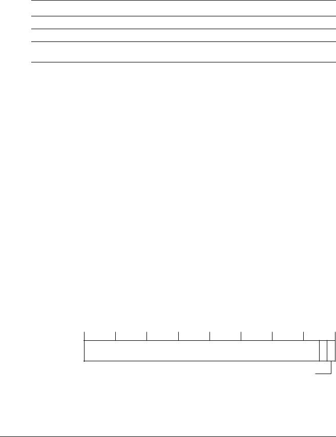
Figure 3-31 Non-Secure Access Control Register format
Table 3-51 lists how the bit values correspond with the Non-Secure Access Control Register functions.
|
|
|
Table 3-51 Non-Secure Access Control Register bit functions |
|
|
|
|
Bits |
Field name |
Function |
|
|
|
|
|
[31:19] |
- |
Reserved. |
|
|
|
UNP/SBZ. |
|
|
|
|
|
[18] |
DMA |
Reserves the DMA channels and registers for the Secure world and determines the page tables, |
|
|
|
Secure or Non-secure, to use for DMA transfers. For details, see DMA on page 7-10: |
|
|
|
0 |
= DMA reserved for the Secure world only and the Secure page tables are used for DMA |
|
|
transfers, reset value |
|
|
|
1 |
= DMA can be used by the Non-secure world and the Non-secure page tables are used for |
|
|
DMA transfers. |
|
|
|
|
|
[17] |
TL |
Prevents operations in the Non-secure world from locking page tables in TLB lockdown |
|
|
|
entries. |
|
|
|
The Invalidate Single Entry or Invalidate ASID match operations can match a TLB lockdown |
|
|
|
entry but an Invalidate All operation only applies to unlocked entries: |
|
|
|
0 |
= Reserve TLB Lockdown registers for Secure operation only, reset value |
|
|
1 |
= TLB Lockdown registers available for Secure and Non-secure operation. |
ARM DDI 0333H |
Copyright © 2004-2009 ARM Limited. All rights reserved. |
3-56 |
ID012410 |
Non-Confidential, Unrestricted Access |
|

|
|
|
System Control Coprocessor |
|
|
|
Table 3-51 Non-Secure Access Control Register bit functions (continued) |
|
|
|
|
Bits |
Field name |
Function |
|
|
|
|
|
[16] |
CL |
Prevents operations in the Non-secure world from changing cache lockdown entries: |
|
|
|
0 |
= Reserve cache lockdown registers for Secure operation only, reset value |
|
|
1 |
= Cache lockdown registers available for Secure and Non-secure operation. |
|
|
|
|
[15:14] |
- |
Reserved. |
|
|
|
UNP/SBZ. |
|
|
|
|
|
[13:0] |
CPna |
Determines permission to access the given coprocessor in the Non-secure world: |
|
|
|
0 |
= Secure access only, reset value |
|
|
1 |
= Secure or Non-secure access. |
a. n is the coprocessor number from 0 to 13.
To use the Non-Secure Access Control Register read or write CP15 with:
•Opcode_1 set to 0
•CRn set to c1
•CRm set to c1
•Opcode_2 set to 2.
For example:
MRC p15, 0, <Rd>, c1, c1, 2 ; Read Non-Secure Access Control Register data
MCR p15, 0, <Rd>, c1, c1, 2 ; Write Non-Secure Access Control Register data
Table 3-52 lists the results of attempted access for each mode.
Table 3-52 Results of access to the Auxiliary Control Register
Secure Privileged |
Non-secure Privileged |
|||
|
|
|
|
User |
Read |
Write |
Read |
Write |
|
|
|
|
|
|
Data |
Data |
Data |
Undefined exception Undefined exception |
|
|
|
|
|
|
3.2.13c2, Translation Table Base Register 0
The purpose of the Translation Table Base Register 0 is to hold the physical address of the first-level translation table.
You use Translation Table Base Register 0 for process-specific addresses, where each process maintains a separate first-level page table. On a context switch you must modify both Translation Table Base Register 0 and the Translation Table Base Control Register, if appropriate.
Table 3-53 on page 3-58 lists the purposes of the individual bits in the Translation Table Base Register 0.
The Translation Table Base Register 0 is:
•in CP15 c2
•a 32 bit read/write register banked for Secure and Non-secure worlds
•accessible in privileged modes only.
Figure 3-32 on page 3-58 shows the bit arrangement for the Translation Table Base Register 0.
ARM DDI 0333H |
Copyright © 2004-2009 ARM Limited. All rights reserved. |
3-57 |
ID012410 |
Non-Confidential, Unrestricted Access |
|

System Control Coprocessor
|
31 |
|
14-N 13-N |
|
5 4 3 2 1 0 |
|
||||||
|
|
Translation table base 0 |
|
UNP/SBZ |
|
RGN |
P |
S |
C |
|
||
|
|
|
|
|
|
|
|
|
|
|
||
|
|
|
|
Figure 3-32 Translation Table Base Register 0 format |
||||||||
|
Table 3-53 lists how the bit values correspond with the Translation Table Base Register 0 |
|||||||||||
|
functions. |
|
|
|
|
|
|
|
|
|
|
|
|
|
|
|
Table 3-53 Translation Table Base Register 0 bit functions |
||||||||
|
|
|
|
|
|
|
|
|
|
|||
Bits |
Field name |
Function |
|
|
|
|
|
|
|
|||
|
|
|
||||||||||
[31:14-N]a |
Translation table base 0 |
Holds the translation table base address, the physical address of the first level |
||||||||||
|
|
|
translation table. The reset value is 0. |
|
|
|
|
|
|
|
||
|
|
|
|
|
|
|
|
|
|
|
||
[13-N:5]a |
- |
|
UNP/SBZ. |
|
|
|
|
|
|
|
||
[4:3] |
RGN |
Indicates the Outer cacheable attributes for page table walking: |
||||||||||
|
|
|
b00 = Outer Noncacheable, reset value |
|
|
|
|
|
|
|
||
|
|
|
b01 = Write-back, Write Allocate |
|
|
|
|
|
|
|
||
|
|
|
b10 = Write-through, No Allocate on Write |
|
|
|
|
|
|
|
||
|
|
|
b11 = Write-back, No Allocate on Write. |
|
|
|
|
|
|
|
||
|
|
|
||||||||||
[2] |
P |
If the processor supports ECC, it indicates to the memory controller it is enabled |
||||||||||
|
|
|
or disabled. For ARM1176JZ-S processors this is 0: |
|
|
|
|
|
|
|||
|
|
|
0 |
= Error-Correcting Code (ECC) is disabled, reset value |
|
|
|
|
|
|
||
|
|
|
1 |
= ECC is enabled. |
|
|
|
|
|
|
|
|
|
|
|
||||||||||
[1] |
S |
Indicates the page table walk is to Non-Shared or to Shared memory: |
||||||||||
|
|
|
0 |
= Non-Shared, reset value |
|
|
|
|
|
|
|
|
|
|
|
1 |
= Shared. |
|
|
|
|
|
|
|
|
|
|
|
||||||||||
[0] |
C |
Indicates the page table walk is Inner Cacheable or Inner Non Cacheable: |
||||||||||
|
|
|
0 |
= Inner Noncacheable, reset value |
|
|
|
|
|
|
|
|
|
|
|
1 |
= Inner cacheable. |
|
|
|
|
|
|
|
|
a. For an explanation of N see c2, Translation Table Base Control Register on page 3-61.
Attempts to write to this register in Secure Privileged mode when CP15SDISABLE is HIGH result in an Undefined exception, see TrustZone write access disable on page 2-9.
Table 3-54 lists the results of attempted access for each mode.
Table 3-54 Results of access to the Translation Table Base Register 0
Secure Privileged |
Non-secure Privileged |
|||
|
|
|
|
User |
Read |
Write |
Read |
Write |
|
|
|
|
|
|
Secure data |
Secure data |
Non-secure data |
Non-secure data Undefined exception |
|
|
|
|
|
|
A write to the Translation Table Base Register 0 updates the address of the first level translation table from the value in bits [31:7] of the written value, to account for the maximum value of 7 for N. The number of bits of this address that the processor uses, and therefore, the required alignment of the first level translation table, depends on the value of N, see c2, Translation Table Base Control Register on page 3-61.
ARM DDI 0333H |
Copyright © 2004-2009 ARM Limited. All rights reserved. |
3-58 |
ID012410 |
Non-Confidential, Unrestricted Access |
|