

- •Contents
- •List of Tables
- •List of Figures
- •Preface
- •About this manual
- •Product revision status
- •Intended audience
- •Using this manual
- •Conventions
- •Additional reading
- •Feedback
- •Feedback on the product
- •Feedback on this book
- •Introduction
- •1.1 About the processor
- •1.2 Extensions to ARMv6
- •1.3 TrustZone security extensions
- •1.4.1 Instruction compression
- •1.4.2 The Thumb instruction set
- •1.4.3 Java bytecodes
- •1.5 Components of the processor
- •1.5.1 Integer core
- •1.5.2 Load Store Unit (LSU)
- •1.5.3 Prefetch unit
- •1.5.4 Memory system
- •1.5.5 AMBA AXI interface
- •1.5.6 Coprocessor interface
- •1.5.7 Debug
- •1.5.8 Instruction cycle summary and interlocks
- •1.5.9 System control
- •1.5.10 Interrupt handling
- •1.6 Power management
- •1.7 Configurable options
- •1.8 Pipeline stages
- •1.9 Typical pipeline operations
- •1.9.1 Instruction progression
- •1.10.1 Extended ARM instruction set summary
- •1.10.2 Thumb instruction set summary
- •1.11 Product revisions
- •Programmer’s Model
- •2.1 About the programmer’s model
- •2.2.1 TrustZone model
- •2.2.2 How the Secure model works
- •2.2.3 TrustZone write access disable
- •2.2.4 Secure Monitor bus
- •2.3 Processor operating states
- •2.3.1 Switching state
- •2.3.2 Interworking ARM and Thumb state
- •2.4 Instruction length
- •2.5 Data types
- •2.6 Memory formats
- •2.7 Addresses in a processor system
- •2.8 Operating modes
- •2.9 Registers
- •2.9.1 The ARM state core register set
- •2.9.2 The Thumb state core register set
- •2.9.3 Accessing high registers in Thumb state
- •2.9.4 ARM state and Thumb state registers relationship
- •2.10 The program status registers
- •2.10.1 The condition code flags
- •2.10.2 The Q flag
- •2.10.4 The GE[3:0] bits
- •2.10.7 The control bits
- •2.10.8 Modification of PSR bits by MSR instructions
- •2.10.9 Reserved bits
- •2.11 Additional instructions
- •2.11.1 Load or Store Byte Exclusive
- •2.11.2 Load or Store Halfword Exclusive
- •2.11.3 Load or Store Doubleword
- •2.11.4 CLREX
- •2.12 Exceptions
- •2.12.1 New instructions for exception handling
- •2.12.2 Exception entry and exit summary
- •2.12.3 Entering an ARM exception
- •2.12.4 Leaving an ARM exception
- •2.12.5 Reset
- •2.12.6 Fast interrupt request
- •2.12.7 Interrupt request
- •2.12.8 Low interrupt latency configuration
- •2.12.9 Interrupt latency example
- •2.12.10 Aborts
- •2.12.11 Imprecise Data Abort mask in the CPSR/SPSR
- •2.12.12 Supervisor call instruction
- •2.12.13 Secure Monitor Call (SMC)
- •2.12.14 Undefined instruction
- •2.12.15 Breakpoint instruction (BKPT)
- •2.12.16 Exception vectors
- •2.12.17 Exception priorities
- •2.13 Software considerations
- •2.13.1 Branch Target Address Cache flush
- •2.13.2 Waiting for DMA to complete
- •System Control Coprocessor
- •3.1 About the system control coprocessor
- •3.1.1 System control coprocessor functional groups
- •3.1.2 System control and configuration
- •3.1.3 MMU control and configuration
- •3.1.4 Cache control and configuration
- •3.1.5 TCM control and configuration
- •3.1.6 Cache Master Valid Registers
- •3.1.7 DMA control
- •3.1.8 System performance monitor
- •3.1.9 System validation
- •3.1.10 Use of the system control coprocessor
- •3.2 System control processor registers
- •3.2.1 Register allocation
- •3.2.2 c0, Main ID Register
- •3.2.3 c0, Cache Type Register
- •3.2.4 c0, TCM Status Register
- •3.2.5 c0, TLB Type Register
- •3.2.6 c0, CPUID registers
- •3.2.7 c1, Control Register
- •3.2.8 c1, Auxiliary Control Register
- •3.2.9 c1, Coprocessor Access Control Register
- •3.2.10 c1, Secure Configuration Register
- •3.2.11 c1, Secure Debug Enable Register
- •3.2.13 c2, Translation Table Base Register 0
- •3.2.14 c2, Translation Table Base Register 1
- •3.2.15 c2, Translation Table Base Control Register
- •3.2.16 c3, Domain Access Control Register
- •3.2.17 c5, Data Fault Status Register
- •3.2.18 c5, Instruction Fault Status Register
- •3.2.19 c6, Fault Address Register
- •3.2.20 c6, Watchpoint Fault Address Register
- •3.2.21 c6, Instruction Fault Address Register
- •3.2.22 c7, Cache operations
- •3.2.23 c8, TLB Operations Register
- •3.2.24 c9, Data and instruction cache lockdown registers
- •3.2.25 c9, Data TCM Region Register
- •3.2.26 c9, Instruction TCM Region Register
- •3.2.29 c9, TCM Selection Register
- •3.2.30 c9, Cache Behavior Override Register
- •3.2.31 c10, TLB Lockdown Register
- •3.2.32 c10, Memory region remap registers
- •3.2.33 c11, DMA identification and status registers
- •3.2.34 c11, DMA User Accessibility Register
- •3.2.35 c11, DMA Channel Number Register
- •3.2.36 c11, DMA enable registers
- •3.2.37 c11, DMA Control Register
- •3.2.38 c11, DMA Internal Start Address Register
- •3.2.39 c11, DMA External Start Address Register
- •3.2.40 c11, DMA Internal End Address Register
- •3.2.41 c11, DMA Channel Status Register
- •3.2.42 c11, DMA Context ID Register
- •3.2.44 c12, Monitor Vector Base Address Register
- •3.2.45 c12, Interrupt Status Register
- •3.2.46 c13, FCSE PID Register
- •3.2.47 c13, Context ID Register
- •3.2.48 c13, Thread and process ID registers
- •3.2.49 c15, Peripheral Port Memory Remap Register
- •3.2.51 c15, Performance Monitor Control Register
- •3.2.52 c15, Cycle Counter Register
- •3.2.53 c15, Count Register 0
- •3.2.54 c15, Count Register 1
- •3.2.55 c15, System Validation Counter Register
- •3.2.56 c15, System Validation Operations Register
- •3.2.57 c15, System Validation Cache Size Mask Register
- •3.2.58 c15, Instruction Cache Master Valid Register
- •3.2.59 c15, Data Cache Master Valid Register
- •3.2.60 c15, TLB lockdown access registers
- •Unaligned and Mixed-endian Data Access Support
- •4.2 Unaligned access support
- •4.2.1 Legacy support
- •4.2.2 ARMv6 extensions
- •4.2.3 Legacy and ARMv6 configurations
- •4.2.4 Legacy data access in ARMv6 (U=0)
- •4.2.5 Support for unaligned data access in ARMv6 (U=1)
- •4.2.6 ARMv6 unaligned data access restrictions
- •4.3 Endian support
- •4.3.1 Load unsigned byte, endian independent
- •4.3.2 Load signed byte, endian independent
- •4.3.3 Store byte, endian independent
- •4.4 Operation of unaligned accesses
- •4.5.1 Legacy fixed instruction and data endianness
- •4.5.3 Reset values of the U, B, and EE bits
- •4.6.1 All load and store operations
- •4.7 Instructions to change the CPSR E bit
- •Program Flow Prediction
- •5.1 About program flow prediction
- •5.2 Branch prediction
- •5.2.1 Enabling program flow prediction
- •5.2.2 Dynamic branch predictor
- •5.2.3 Static branch predictor
- •5.2.4 Branch folding
- •5.2.5 Incorrect predictions and correction
- •5.3 Return stack
- •5.4 Memory Barriers
- •5.4.1 Instruction Memory Barriers (IMBs)
- •5.5.1 Execution of IMB instructions
- •Memory Management Unit
- •6.1 About the MMU
- •6.2 TLB organization
- •6.2.1 MicroTLB
- •6.2.2 Main TLB
- •6.2.3 TLB control operations
- •6.2.5 Supersections
- •6.3 Memory access sequence
- •6.3.1 TLB match process
- •6.3.2 Virtual to physical translation mapping restrictions
- •6.4 Enabling and disabling the MMU
- •6.4.1 Enabling the MMU
- •6.4.2 Disabling the MMU
- •6.4.3 Behavior with MMU disabled
- •6.5 Memory access control
- •6.5.1 Domains
- •6.5.2 Access permissions
- •6.5.3 Execute never bits in the TLB entry
- •6.6 Memory region attributes
- •6.6.1 C and B bit, and type extension field encodings
- •6.6.2 Shared
- •6.6.3 NS attribute
- •6.7 Memory attributes and types
- •6.7.1 Normal memory attribute
- •6.7.2 Device memory attribute
- •6.7.3 Strongly Ordered memory attribute
- •6.7.4 Ordering requirements for memory accesses
- •6.7.5 Explicit Memory Barriers
- •6.7.6 Backwards compatibility
- •6.8 MMU aborts
- •6.8.1 External aborts
- •6.9 MMU fault checking
- •6.9.1 Fault checking sequence
- •6.9.2 Alignment fault
- •6.9.3 Translation fault
- •6.9.4 Access bit fault
- •6.9.5 Domain fault
- •6.9.6 Permission fault
- •6.9.7 Debug event
- •6.10 Fault status and address
- •6.11 Hardware page table translation
- •6.11.2 ARMv6 page table translation subpage AP bits disabled
- •6.11.3 Restrictions on page table mappings page coloring
- •6.12 MMU descriptors
- •Level One Memory System
- •7.1 About the level one memory system
- •7.2 Cache organization
- •7.2.1 Features of the cache system
- •7.2.2 Cache functional description
- •7.2.3 Cache control operations
- •7.2.4 Cache miss handling
- •7.2.5 Cache disabled behavior
- •7.2.6 Unexpected hit behavior
- •7.3.1 TCM behavior
- •7.3.2 Restriction on page table mappings
- •7.3.3 Restriction on page table attributes
- •7.5 TCM and cache interactions
- •7.5.1 Overlapping between TCM regions
- •7.5.2 DMA and core access arbitration
- •7.5.3 Instruction accesses to TCM
- •7.5.4 Data accesses to the Instruction TCM
- •7.6 Write buffer
- •Level Two Interface
- •8.1 About the level two interface
- •8.1.1 AXI parameters for the level 2 interconnect interfaces
- •8.2 Synchronization primitives
- •8.2.3 Example of LDREX and STREX usage
- •8.3 AXI control signals in the processor
- •8.3.1 Channel definition
- •8.3.2 Signal name suffixes
- •8.3.3 Address channel signals
- •8.4 Instruction Fetch Interface transfers
- •8.4.1 Cacheable fetches
- •8.4.2 Noncacheable fetches
- •8.5 Data Read/Write Interface transfers
- •8.5.1 Linefills
- •8.5.2 Noncacheable LDRB
- •8.5.3 Noncacheable LDRH
- •8.5.4 Noncacheable LDR or LDM1
- •8.5.5 Noncacheable LDRD or LDM2
- •8.5.6 Noncacheable LDM3
- •8.5.7 Noncacheable LDM4
- •8.5.8 Noncacheable LDM5
- •8.5.9 Noncacheable LDM6
- •8.5.10 Noncacheable LDM7
- •8.5.11 Noncacheable LDM8
- •8.5.12 Noncacheable LDM9
- •8.5.13 Noncacheable LDM10
- •8.5.14 Noncacheable LDM11
- •8.5.15 Noncacheable LDM12
- •8.5.16 Noncacheable LDM13
- •8.5.17 Noncacheable LDM14
- •8.5.18 Noncacheable LDM15
- •8.5.19 Noncacheable LDM16
- •8.6 Peripheral Interface transfers
- •8.7 Endianness
- •8.8 Locked access
- •Clocking and Resets
- •9.1 About clocking and resets
- •9.2 Clocking and resets with no IEM
- •9.2.1 Processor clocking with no IEM
- •9.2.2 Reset with no IEM
- •9.3 Clocking and resets with IEM
- •9.3.1 Processor clocking with IEM
- •9.3.2 Reset with IEM
- •9.4 Reset modes
- •9.4.1 Power-on reset
- •9.4.2 CP14 debug logic
- •9.4.3 Processor reset
- •9.4.4 DBGTAP reset
- •9.4.5 Normal operation
- •Power Control
- •10.1 About power control
- •10.2 Power management
- •10.2.1 Run mode
- •10.2.2 Standby mode
- •10.2.3 Shutdown mode
- •10.2.4 Dormant mode
- •10.2.5 Communication to the Power Management Controller
- •10.3 Intelligent Energy Management
- •10.3.1 Purpose of IEM
- •10.3.2 Structure of IEM
- •10.3.3 Operation of IEM
- •Coprocessor Interface
- •11.1 About the coprocessor interface
- •11.2 Coprocessor pipeline
- •11.2.1 Coprocessor instructions
- •11.2.2 Coprocessor control
- •11.2.3 Pipeline synchronization
- •11.2.4 Pipeline control
- •11.2.5 Instruction tagging
- •11.2.6 Flush broadcast
- •11.3 Token queue management
- •11.3.1 Queue implementation
- •11.3.2 Queue modification
- •11.3.3 Queue flushing
- •11.4 Token queues
- •11.4.1 Instruction queue
- •11.4.2 Length queue
- •11.4.3 Accept queue
- •11.4.4 Cancel queue
- •11.4.5 Finish queue
- •11.5 Data transfer
- •11.5.1 Loads
- •11.5.2 Stores
- •11.6 Operations
- •11.6.1 Normal operation
- •11.6.2 Cancel operations
- •11.6.3 Bounce operations
- •11.6.4 Flush operations
- •11.6.5 Retirement operations
- •11.7 Multiple coprocessors
- •11.7.1 Interconnect considerations
- •11.7.2 Coprocessor selection
- •11.7.3 Coprocessor switching
- •Vectored Interrupt Controller Port
- •12.1 About the PL192 Vectored Interrupt Controller
- •12.2 About the processor VIC port
- •12.2.1 Synchronization of the VIC port signals
- •12.2.2 Interrupt handler exit
- •12.3 Timing of the VIC port
- •12.3.1 PL192 VIC timing
- •12.3.2 Core timing
- •12.4 Interrupt entry flowchart
- •Debug
- •13.1 Debug systems
- •13.1.1 The debug host
- •13.1.2 The protocol converter
- •13.1.3 The processor
- •13.2 About the debug unit
- •13.2.3 Secure Monitor mode and debug
- •13.2.4 Virtual addresses and debug
- •13.2.5 Programming the debug unit
- •13.3 Debug registers
- •13.3.1 Accessing debug registers
- •13.3.2 CP14 c0, Debug ID Register (DIDR)
- •13.3.3 CP14 c1, Debug Status and Control Register (DSCR)
- •13.3.4 CP14 c5, Data Transfer Registers (DTR)
- •13.3.5 CP14 c6, Watchpoint Fault Address Register (WFAR)
- •13.3.6 CP14 c7, Vector Catch Register (VCR)
- •13.3.10 CP14 c112-c113, Watchpoint Control Registers (WCR)
- •13.3.11 CP14 c10, Debug State Cache Control Register
- •13.3.12 CP14 c11, Debug State MMU Control Register
- •13.4 CP14 registers reset
- •13.5 CP14 debug instructions
- •13.5.1 Executing CP14 debug instructions
- •13.6 External debug interface
- •13.7 Changing the debug enable signals
- •13.8 Debug events
- •13.8.1 Software debug event
- •13.8.2 External debug request signal
- •13.8.3 Halt DBGTAP instruction
- •13.8.4 Behavior of the processor on debug events
- •13.8.5 Effect of a debug event on CP15 registers
- •13.9 Debug exception
- •13.10 Debug state
- •13.10.1 Behavior of the PC in Debug state
- •13.10.2 Interrupts
- •13.10.3 Exceptions
- •13.11 Debug communications channel
- •13.12 Debugging in a cached system
- •13.12.1 Data cache writes
- •13.13 Debugging in a system with TLBs
- •13.14 Monitor debug-mode debugging
- •13.14.1 Entering the debug monitor target
- •13.14.2 Setting breakpoints, watchpoints, and vector catch debug events
- •13.14.3 Setting software breakpoint debug events (BKPT)
- •13.14.4 Using the debug communications channel
- •13.15 Halting debug-mode debugging
- •13.15.1 Entering Debug state
- •13.15.2 Exiting Debug state
- •13.15.3 Programming debug events
- •13.16 External signals
- •Debug Test Access Port
- •14.1 Debug Test Access Port and Debug state
- •14.2 Synchronizing RealView ICE
- •14.3 Entering Debug state
- •14.4 Exiting Debug state
- •14.5 The DBGTAP port and debug registers
- •14.6 Debug registers
- •14.6.1 Bypass register
- •14.6.2 Device ID code register
- •14.6.3 Instruction register
- •14.6.4 Scan chain select register (SCREG)
- •14.6.5 Scan chains
- •14.6.6 Reset
- •14.7 Using the Debug Test Access Port
- •14.7.1 Entering and leaving Debug state
- •14.7.2 Executing instructions in Debug state
- •14.7.3 Using the ITRsel IR instruction
- •14.7.4 Transferring data between the host and the core
- •14.7.5 Using the debug communications channel
- •14.7.6 Target to host debug communications channel sequence
- •14.7.7 Host to target debug communications channel
- •14.7.8 Transferring data in Debug state
- •14.7.9 Example sequences
- •14.8 Debug sequences
- •14.8.1 Debug macros
- •14.8.2 General setup
- •14.8.3 Forcing the processor to halt
- •14.8.4 Entering Debug state
- •14.8.5 Leaving Debug state
- •14.8.8 Reading the CPSR/SPSR
- •14.8.9 Writing the CPSR/SPSR
- •14.8.10 Reading the PC
- •14.8.11 Writing the PC
- •14.8.12 General notes about reading and writing memory
- •14.8.13 Reading memory as words
- •14.8.14 Writing memory as words
- •14.8.15 Reading memory as halfwords or bytes
- •14.8.16 Writing memory as halfwords/bytes
- •14.8.17 Coprocessor register reads and writes
- •14.8.18 Reading coprocessor registers
- •14.8.19 Writing coprocessor registers
- •14.9 Programming debug events
- •14.9.1 Reading registers using scan chain 7
- •14.9.2 Writing registers using scan chain 7
- •14.9.3 Setting breakpoints, watchpoints and vector traps
- •14.9.4 Setting software breakpoints
- •14.10 Monitor debug-mode debugging
- •14.10.1 Receiving data from the core
- •14.10.2 Sending data to the core
- •Trace Interface Port
- •15.1 About the ETM interface
- •15.1.1 Instruction interface
- •15.1.2 Secure control bus
- •15.1.3 Data address interface
- •15.1.4 Data value interface
- •15.1.5 Pipeline advance interface
- •15.1.6 Coprocessor interface
- •15.1.7 Other connections to the core
- •Cycle Timings and Interlock Behavior
- •16.1 About cycle timings and interlock behavior
- •16.1.1 Changes in instruction flow overview
- •16.1.2 Instruction execution overview
- •16.1.3 Conditional instructions
- •16.1.4 Opposite condition code checks
- •16.1.5 Definition of terms
- •16.2 Register interlock examples
- •16.3 Data processing instructions
- •16.3.1 Cycle counts if destination is not PC
- •16.3.2 Cycle counts if destination is the PC
- •16.3.3 Example interlocks
- •16.4 QADD, QDADD, QSUB, and QDSUB instructions
- •16.6 ARMv6 Sum of Absolute Differences (SAD)
- •16.6.1 Example interlocks
- •16.7 Multiplies
- •16.8 Branches
- •16.9 Processor state updating instructions
- •16.10 Single load and store instructions
- •16.10.1 Base register update
- •16.11 Load and Store Double instructions
- •16.12 Load and Store Multiple Instructions
- •16.12.1 Load and Store Multiples, other than load multiples including the PC
- •16.12.2 Load Multiples, where the PC is in the register list
- •16.12.3 Example Interlocks
- •16.13 RFE and SRS instructions
- •16.14 Synchronization instructions
- •16.15 Coprocessor instructions
- •16.16 SVC, SMC, BKPT, Undefined, and Prefetch Aborted instructions
- •16.17 No operation
- •16.18 Thumb instructions
- •AC Characteristics
- •17.1 Processor timing diagrams
- •17.2 Processor timing parameters
- •Signal Descriptions
- •A.1 Global signals
- •A.2 Static configuration signals
- •A.3 TrustZone internal signals
- •A.4 Interrupt signals, including VIC interface
- •A.5 AXI interface signals
- •A.5.1 Instruction read port signals
- •A.5.2 Data port signals
- •A.5.3 Peripheral port signals
- •A.5.4 DMA port signals
- •A.6 Coprocessor interface signals
- •A.7 Debug interface signals, including JTAG
- •A.8 ETM interface signals
- •A.9 Test signals
- •B.1 About the differences between the ARM1136J-S and ARM1176JZ-S processors
- •B.2 Summary of differences
- •B.2.1 TrustZone
- •B.2.2 ARMv6k extensions support
- •B.2.3 Power management
- •B.2.4 SmartCache
- •B.2.7 Tightly-Coupled Memories
- •B.2.8 Fault Address Register
- •B.2.9 Fault Status Register
- •B.2.10 Prefetch Unit
- •B.2.11 System control coprocessor operations
- •B.2.13 Debug
- •B.2.14 Level two interface
- •B.2.15 Memory BIST
- •Revisions
- •Glossary
Coprocessor Interface
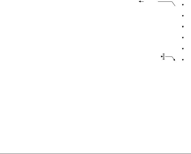
11.5Data transfer
Data transfers are managed by the LSU on the core side, and the pipeline itself on the coprocessor side. Transfers can be a single value or a vector. In the latter case, the coprocessor effectively converts a multiple transfer into a series of single transfers by iterating the instruction in the issue stage. This creates an instance of the load/store instruction for each item to be transferred.
The instruction stays in the coprocessor issue stage while it iterates, creating copies of itself that move down the pipeline. Figure 11-9 on page 11-16 illustrates this process for a load instruction.
The first of the iterated instructions, shown in uppercase, is the head and the others, shown in lowercase, are the tails. In the example shown the vector length is four so there is one head and three tails. At the first iteration of the instruction, the tail flag is set so that subsequent iterations send tail instructions down the pipeline. In the example shown in Figure 11-9 on page 11-16, instruction B has stalled in the Ex1 stage, that might be caused by the cancel queue being empty, so that instruction C does not iterate during its first cycle in the issue stage, but only starts to iterate after the stall has been removed.
Figure 11-8 shows the extra paths required for passing data to and from the coprocessor.
|
|
|
|
|
|
|
|
|
|
I |
|
To LSU Add stage |
|
|
|
|
|
|
|
|
|
|
|
|
|
|
|
|
|
||||||
Store data |
|||||||||||
|
|
|
|
|
|
|
|
|
|
|
|
|
|
|
|
|
|
|
|
|
|
Ex1 |
|
|
|
|
|
|
|
|
|
|
|
|
|
|
|
|
|
|
|
|
|
|
|
|
|
|
|
|
|
|
|
|
|
|
|
|
|
|
|
|
|
|
|
|
|
|
|
Ex2 |
|
|
|
|
|
|
|
|
|
|
|
|
|
|
|
|
|
|
|
|
|
|
|
|
|
|
|
|
|
|
|
|
|
|
|
|
|
|
|
|
|
|
|
|
|
|
|
Ex3 |
|
|
|
|
|
|
|
|
|
|
|
|
|
|
|
|
|
|
|
|
|
|
|
|
|
|
|
|
|
|
|
|
|
|
|
|
|
|
|
|
|
|
|
|
|
|
|
Ex4 |
|
|
|
|
|
|
|
|
|
|
|
|
|
|
|
|
|
|
|
|
|
|
|
|
|
|
|
|
|
|
|
|
|
|
|
|
|
From LSU Wbls stage |
|
|
|
|
|
|
|
|
|
Ex5 |
|
|
|
Load data |
|
|
|
|
|
|
|
|
|
|
|
|
|
|
|||||||
|
|
|
|
|
|
|
|
|
|
|
|
|
|
|
|
|
|
|
|
|
|
Ex6 |
|
|
|
|
|
|
|
|
|
|
|
|
|
Figure 11-8 Coprocessor data transfer
Two data paths are required:
•One passes store data from the coprocessor to the core, and this requires a queue, that is maintained by the core.
•The other passes load data from the core to the coprocessor and requires no queue, only two pipeline registers.
Figure 11-9 on page 11-16 shows instruction iteration for loads.
ARM DDI 0333H |
Copyright © 2004-2009 ARM Limited. All rights reserved. |
11-15 |
ID012410 |
Non-Confidential, Unrestricted Access |
|
Coprocessor Interface
I |
A |
B |
[C] |
C |
c |
c |
c |
D |
|
|
|
|
|
|
Ex1 |
|
|
|
|
|
|
|
|
|
|
|
|
|
|
|
A |
[B] |
B |
C |
c |
c |
c |
D |
|
|
|
|
|
|
Ex2 |
|
|
|
|
|
|
|
|
|
|
|
|
|
|
|
|
A |
|
B |
C |
c |
c |
c |
D |
|
|
|
|
|
Ex3 |
|
|
|
A |
|
B |
C |
c |
c |
c |
D |
|
|
|
|
|
|
|
|
|
|
||||||||
Ex4 |
|
|
|
|
A |
|
B |
C |
c |
c |
c |
D |
|
|
|
|
|
|
|
|
|
||||||||
Ex5 |
|
|
|
|
|
A |
|
B |
C |
c |
c |
c |
D |
|
|
|
|
|
|
|
|
||||||||
Ex6 |
|
|
|
|
|
|
A |
|
B |
C |
c |
c |
c |
D |
|
|
|
|
|
|
|
||||||||
|
|
|
|
|
|
|
|
|
|
|
|
|
|
|
Time |
1 |
2 |
3 |
4 |
5 |
6 |
7 |
8 |
9 |
10 |
11 |
12 |
13 |
14 |
Figure 11-9 Instruction iteration for loads
Only the head instruction is involved in token exchange with the core pipeline, that does not iterate instructions in this way, the tail instructions passing down the pipeline silently.
When an iterated load/store instruction is cancelled or flushed, all the tail instructions, bearing the same tag, must be removed from the pipeline. Only the head instruction becomes a phantom when cancelled. Any tail instruction can be left intact in the pipeline because it has no other effect.
Because the cancel token is received in the coprocessor Ex1 stage, a cancelled iterated instruction always consists of a head instruction in Ex1 and a single tail instruction in the issue stage.
11.5.1Loads
Load data emerge from the WBls stage of the core LSU and are received by the coprocessor Ex6 stage. Each item in a vectored load is picked up by one instance of the iterated load instruction.
The pipeline timing means that a load instruction is always ready, or arrived a short time ago, in Ex6 to pick up each data item. If a load instruction has arrived in Ex6, but the load information has not yet appeared, the load instruction must stall in Ex6, stalling the rest of the coprocessor pipeline.
The following signals are driven by the core to pass load data across to the coprocessor:
ACPLDVALID
This signal, when set, indicates that the associated data are valid.
ACPLDDATA[63:0]
This is the information passed from the core to the coprocessor.
Load buffers
To achieve correct alignment of the load data with the load instruction in the coprocessor Ex6 stage, the data must be double buffered when they arrive at the coprocessor. Figure 11-10 on page 11-17 shows an example.
ARM DDI 0333H |
Copyright © 2004-2009 ARM Limited. All rights reserved. |
11-16 |
ID012410 |
Non-Confidential, Unrestricted Access |
|

|
|
|
|
|
|
|
|
Coprocessor Interface |
|||||
WBls |
|
|
|
|
|
|
|
|
|
|
|
|
Ex6 |
Data |
|
|
|
|
Interconnect |
|
|
|
|
|
|
|
Data |
|
|
|
|
|
|
|
|
|
|||||
Valid |
|
|
|
|
Interconnect |
|
|
|
|
|
|
|
Valid |
|
|
|
|
|
|
|
|
|
|
|
|||
|
|
|
|
|
|
|
|
|
|
|
|||
|
|
|
|
|
|
|
|
|
|
|
|||
|
|
|
|
|
|
|
|
|
|
||||
|
|
Core |
Coprocessor |
||||||||||
Figure 11-10 Load data buffering
The load data buffers function as pipeline registers and so require no flow control and are not required to carry any tags. Only the data and a valid bit are required. For load transfers to work:
•instructions must always arrive in the coprocessor Ex6 stage coincident with, or before, the arrival of the corresponding instruction in the core WBls stage
•finish tokens from the core must arrive at the same time as the corresponding load data items arrive at the end of the load data pipeline buffers
•the LSU must see the token from the accept queue before it enables a load instruction to move on from its Add stage.
Loads and flushes
If a flush does not involve the core WBls stage it cannot affect the load data buffers, and the load transfer completes normally. If a flush is initiated by an instruction in the core WBls stage, this is not a load instruction because load instructions cannot trigger a flush. Any coprocessor load instructions behind the flush point find themselves stalled if they get as far as the Ex6 stage, for the lack of a finish token, so no data transfers can have taken place. Any data in the load data buffers expires naturally during the flush dead period while the pipeline reloads.
Loads and cancels
If a load instruction is canceled both the head and any tails must be removed. Because the cancellation happens in the coprocessor Ex1 stage, no data transfers can have taken place and therefore no special measures are required to deal with load data.
Loads and retirement
When a load instruction reaches the bottom of the coprocessor pipeline it must find a data item at the end of the load data buffer. This applies to both head and tail instructions. Load instructions do not use finish queue.
11.5.2Stores
Store data emerge from the coprocessor issue stage and are received by the core LSU DC1 stage. Each item of a vectored store is generated because the store instruction iterates in the coprocessor issue stage. The iterated store instructions then pass down the pipeline but have no other use, except to act as place markers for flushes and cancels.
ARM DDI 0333H |
Copyright © 2004-2009 ARM Limited. All rights reserved. |
11-17 |
ID012410 |
Non-Confidential, Unrestricted Access |
|

Coprocessor Interface
The following signals control the transfer of store data across the coprocessor interface:
CPASTDATAV
This signal is asserted when valid data is available from the coprocessor.
CPASTDATAT[3:0]
This is the tag associated with the data being passed to the core.
CPASTDATA[63:0]
This is the information passed from the coprocessor to the core.
ACPSTSTOP
This signal from the core prevents additional transfers from the coprocessor to the core, and is raised when the store queue, maintained by the core, can no longer accept any more data. When the signal is deasserted, data transfers can resume.
When ACPSTSTOP is asserted, the data previously placed onto CPASTDATA
must be left there, until new data can be transferred. This enables the core to leave data on CPASTDATA until there is sufficient space in the store data queue.
Store data queue
Because the store data transfer can be stopped at any time by the LSU, a store data queue is required. Additionally, because store data vectors can be of arbitrary length, flow control is required. A queue length of three slots is sufficient to enable flow control to be used without loss of data.
Stores and flushes
When a store instruction is involved in a flush, the store data queue must be flushed by the core. Because the queue continues to fill for two cycles after the core notifies the coprocessor of the flush, because of the signal propagation delay, the core must delay for two cycles before carrying out the store data queue flush. The dead period after the flush extends sufficiently far to enable this to be done.
Stores and cancels
If the core cancels a store instruction, the coprocessor must ensure that it sends no store data for that instruction. It can achieve this by either:
•delaying the start of the store data until the corresponding cancel token has been received in the Ex1 stage
•looking ahead into the cancel queue and start the store data transfer when the correct token is seen.
Stores and retirement
Because store instructions do not use the finish token queue they are retired as soon as they leave the Ex1 stage of the pipeline.
ARM DDI 0333H |
Copyright © 2004-2009 ARM Limited. All rights reserved. |
11-18 |
ID012410 |
Non-Confidential, Unrestricted Access |
|