


System Control Coprocessor
Note
When the SCR EA bit is set, see c1, Secure Configuration Register on page 3-52, the processor writes to the Secure Instruction Fault Status Register on a Secure Monitor entry caused by an external abort.
To use the IFSR read or write CP15 with:
•Opcode_1 set to 0
•CRn set to c5
•CRm set to c0
•Opcode_2 set to 1.
For example:
MRC p15, 0, <Rd>, c5, c0, 1 ; Read Instruction Fault Status Register
MCR p15, 0, <Rd>, c5, c0, 1 ; Write Instruction Fault Status Register
3.2.19c6, Fault Address Register
The purpose of the Fault Address Register (FAR) is to hold the Modified Virtual Address (MVA) of the fault when a precise abort occurs.
The FAR is:
•in CP15 c6
•a 32-bit read/write register banked for Secure and Non-secure worlds
•accessible in privileged modes only.
The Fault Address Register bits [31:0] contain the MVA that the precise abort occurred on. The reset value is 0.
Table 3-65 lists the results of attempted access for each mode.
Table 3-65 Results of access to the Fault Address Register
Secure Privileged |
Non-secure Privileged |
||
|
|
|
User |
Read |
Write |
Read |
Write |
|
|
|
|
Secure data |
Secure data |
Non-secure data |
Non-secure data Undefined exception |
|
|
|
|
To use the FAR read or write CP15 with:
•Opcode_1 set to 0
•CRn set to c6
•CRm set to c0
•Opcode_2 set to 0.
For example:
MRC |
p15, |
0, |
<Rd>, |
c6, |
c0, |
0 |
; |
Read Fault Address Register |
MCR |
p15, |
0, |
<Rd>, |
c6, |
c0, |
0 |
; |
Write Fault Address Register |
A write to this register sets the FAR to the value of the data written. This is useful for a debugger to restore the value of the FAR.
The ARM1176JZ-S processor also updates the FAR on debug exception entry because of watchpoints, see Effect of a debug event on CP15 registers on page 13-34 for more details.
ARM DDI 0333H |
Copyright © 2004-2009 ARM Limited. All rights reserved. |
3-68 |
ID012410 |
Non-Confidential, Unrestricted Access |
|

System Control Coprocessor
3.2.20c6, Watchpoint Fault Address Register
Access to the Watchpoint Fault Address register through the system control coprocessor is deprecated, see CP14 c6, Watchpoint Fault Address Register (WFAR) on page 13-12.
3.2.21c6, Instruction Fault Address Register
The purpose of the Instruction Fault Address Register (IFAR) is to hold the address of instructions that cause a prefetch abort.
The IFAR is:
•in CP15 c6
•a 32-bit read/write register banked for Secure and Non-secure worlds
•accessible in privileged modes only.
The Instruction Fault Address Register bits [31:0] contain the Instruction Fault MVA. The reset value is 0.
Table 3-66 lists the results of attempted access for each mode.
Table 3-66 Results of access to the Instruction Fault Address Register
Secure Privileged |
Non-secure Privileged |
||
|
|
|
User |
Read |
Write |
Read |
Write |
|
|
|
|
Secure data |
Secure data |
Non-secure data |
Non-secure data Undefined exception |
|
|
|
|
To use the IFAR read or write CP15 with:
•Opcode_1 set to 0
•CRn set to c6
•CRm set to c0
•Opcode_2 set to 2.
For example:
MRC p15, 0, <Rd>, c6, c0, 2 ; Read Instruction Fault Address Register
MCR p15, 0, <Rd>, c6, c0, 2 ; Write Instruction Fault Address Register
A write to this register sets the IFAR to the value of the data written. This is useful for a debugger to restore the value of the IFAR.
3.2.22c7, Cache operations
The purpose of c7 is to:
•control these operations:
—clean and invalidate instruction and data caches, including range operations
—prefetch instruction cache line
—Flush Prefetch Buffer
—flush branch target address cache
—virtual to physical address translation.
•implement the Data Synchronization Barrier (DSB) operation
•implement the Data Memory Barrier (DMB) operation
ARM DDI 0333H |
Copyright © 2004-2009 ARM Limited. All rights reserved. |
3-69 |
ID012410 |
Non-Confidential, Unrestricted Access |
|
System Control Coprocessor
•implement the Wait For Interrupt clock control function.
Note
Cache operations also depend on:
•the C, W, I and RR bits, see c1, Control Register on page 3-44.
•the RA and RV bits, see c1, Auxiliary Control Register on page 3-49.
The following cache operations globally flush the BTAC:
•Invalidate Entire Instruction Cache
•Invalidate Both Caches.
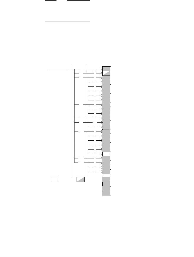
c7 consists of one 32-bit register that performs 28 functions. Figure 3-38 shows the arrangement of the 24 functions in this group that operate with the MCR and MRC instructions.
CRn |
Opcode_1 CRm Opcode_2 |
c7 |
0 |
c0 |
4 |
SBZ |
|
|
c4 |
0 |
|
|
|
c5 |
0 |
SBZ |
|
|
|
1 |
MVA |
|
|
|
2 |
Index |
|
|
|
4 |
SBZ |
|
|
|
6 |
SBZ |
|
|
|
7 |
MVA |
|
|
c6 |
0 |
SBZ |
|
|
|
1 |
MVA |
|
|
|
2 |
Index |
|
|
c7 |
0 |
SBZ |
|
|
c8 |
0-3 |
|
|
|
|
4-7 |
|
|
|
c10 |
0 |
SBZ |
|
|
|
1 |
MVA |
|
|
|
2 |
Index |
|
|
|
4 |
SBZ |
|
|
|
5 |
SBZ |
|
|
|
6 |
|
|
|
c13 |
1 |
MVA |
|
|
c14 |
0 |
SBZ |
|
|
|
1 |
MVA |
|
|
|
2 |
Index |
Wait For Interrupt (WFI) PA Register
Invalidate Entire Instruction Cache
Invalidate Instruction Cache Line (using MVA) Invalidate Instruction Cache Line (using Index)
Flush Prefetch Buffer
Flush Entire Branch Target Cache
Flush Branch Target Cache Entry Invalidate Entire Data Cache
Invalidate Data Cache Line (using MVA) Invalidate Data Cache Line (using Index) Invalidate Both Caches
VA to PA Translation in the current world VA to PA Translation in the other world Clean Entire Data Cache
Clean Data Cache Line (using MVA)
Clean Data Cache Line (using Index)
Data Synchronization Barrier (DSB) Data Memory Barrier (DMB)
Cache Dirty Status Register Prefetch Instruction Cache Line
Clean and Invalidate Entire Data Cache
Clean and Invalidate Data Cache Line (using MVA) Clean and Invalidate Data Cache Line (using Index)
Read-only |
Read/write |
|
SBZ |
|
MVA |
|
Index |
Write only Accessible in User mode
Should Be Zero Using MVA
Using Set and Index
Figure 3-38 Cache operations
Figure 3-39 on page 3-71 shows the arrangement of the 4 functions in this group that operate with the MCRR instruction.
ARM DDI 0333H |
Copyright © 2004-2009 ARM Limited. All rights reserved. |
3-70 |
ID012410 |
Non-Confidential, Unrestricted Access |
|

System Control Coprocessor
Opcode_1 CRm
0 |
|
|
|
|
c5 |
|
|
|
|
||
|
|
|
|
|
|
||||||
|
|
|
|
|
|
|
|
||||
|
|
|
|
|
c6 |
|
|
|
|
|
|
|
|
|
|
|
|
||||||
|
|
|
|
|
|
|
|
|
|
|
|
|
|
|
|
c12 |
|
|
|
|
|||
|
|
|
|
|
|
||||||
|
|
|
|
|
|
|
|
|
|
|
|
|
|
|
|
c14 |
|
|
|
|
|||
Read-only |
|
|
|
|
|||||||
|
|
|
|
|
|
Read/write |
|||||
|
|
|
|
|
|
||||||
VA Invalidate Instruction Cache Range
VA Invalidate Data Cache Range
VA Clean Data Cache Range
VA Clean and Invalidate Data Cache Range
VA Using VA Accessible in User mode
Figure 3-39 Cache operations with MCRR instructions
Note
•Writing c7 with a combination of CRm and Opcode_2 not listed in Figure 3-38 on page 3-70 or CRm not listed in Figure 3-39 results in an Undefined exception apart from the following operations, that are architecturally defined as unified cache operations and have no effect:
—MCR p15,0,<Rd>,c7,c7,{1-7}
—MCR p15,0,<Rd>,c7,c11,{0-7}
—MCR p15,0,<Rd>,c7,c15,{0-7}.
•In the ARM1176JZ-S processor, reading from c7, except for reads from the Cache Dirty Status Register or PA Register, causes an Undefined instruction trap.
•Writes to the Cache Dirty Status Register cause an Undefined exception.
•If Opcode_1 = 0, these instructions are applied to a level one cache system. All other Opcode_1 values are reserved.
•All accesses to c7 can only be executed in a privileged mode of operation, except Data Synchronization Barrier, Flush Prefetch Buffer, Data Memory Barrier, and Clean Data Cache Range. These can be operated in User mode. Attempting to execute a privileged instruction in User mode results in the Undefined instruction trap being taken.
There are three ways to use c7:
•For the Cache Dirty Status Register, read c7 with the MRC instruction.
•For range operations use the MCRR instruction with the value of CRm to select the required operation.
•For all other operations use the MCR instruction to write to c7 with the combination of CRm and Opcode_2 to select the required operation.
Depending on the operation you require set <Rd> for MCR instructions or <Rd> and <Rn> for MCRR instructions to:
—Virtual Address (VA)
—Modified Virtual Address (MVA)
—Set and Index
—Should Be Zero.
Invalidate, Clean, and Prefetch operations
The purposes of the invalidate, clean, and prefetch operations that c7 provides are to:
•Invalidate part or all of the Data or Instruction caches
•Clean part or all of the Data cache
•Clean and Invalidate part or all of the Data cache
ARM DDI 0333H |
Copyright © 2004-2009 ARM Limited. All rights reserved. |
3-71 |
ID012410 |
Non-Confidential, Unrestricted Access |
|

System Control Coprocessor
•Prefetch code into the Instruction cache.
The terms used to describe the invalidate, clean, and prefetch operations are as defined in the
Caches and Write Buffers chapter of the ARM Architecture Reference Manual.
For details of the behavior of c7 in the Secure and Non-secure worlds, see TrustZone behavior on page 3-77.
When it controls invalidate, clean, and prefetch operations c7 appears as a 32-bit write only register. There are four possible formats for the data that you write to the register that depend on the specific operation:
•Set and Index format
•MVA
•VA
•SBZ.
Set and Index format
Figure 3-40 shows the Set and Index format for invalidate and clean operations.
31 30 29 |
|
S+5 |
S+4 |
|
5 |
4 |
1 |
0 |
|
|
|
|
|
|
|
|
|
|
|
Set |
|
SBZ/UNP |
|
|
Index |
|
SBZ/UNP |
0 |
|
|
|
|
|
|
|
|
|
|
|
Figure 3-40 c7 format for Set and Index
Table 3-67 lists how the bit values correspond with the Cache Operation functions for Set and Index format operations.
|
|
Table 3-67 Functional bits of c7 for Set and Index |
|
|
|
Bits |
Field name |
Function |
|
|
|
[31:30] |
Set |
Selects the cache set to operate on, from the four cache sets. |
|
|
Value is the cache set number. |
|
|
|
[29:S+5] |
- |
UNP/SBZ. |
|
|
|
[S+4:5] |
Index |
Selects the cache line to operate on. |
|
|
Value is the index number. |
|
|
|
[4:1] |
- |
SBZ. |
|
|
|
[0] |
0 |
For the ARM1176JZ-S, this Should Be Zero. |
|
|
|
The value of S in Table 3-68 depends on the cache size. Table 3-68 lists the relationship of cache sizes and S.
Table 3-68 Cache size and S parameter dependency
|
Cache size |
S |
|
|
|
|
4KB |
5 |
|
|
|
|
8KB |
6 |
|
|
|
|
16KB |
7 |
|
|
|
|
32KB |
8 |
|
|
|
|
64KB |
9 |
|
|
|
|
|
|
ARM DDI 0333H |
Copyright © 2004-2009 ARM Limited. All rights reserved. |
3-72 |
ID012410 |
Non-Confidential, Unrestricted Access |
|
System Control Coprocessor
The value of S is given by:
S = log2
cache size
Associativity x line length in bytes
See c0, Cache Type Register on page 3-21 for details of instruction and data cache size.
Note
If the data is stated to be Set and Index format, see Figure 3-40 on page 3-72, it identifies the cache line that the operation applies to by specifying the cache Set that it belongs to and what its Index is within the Set. The Set corresponds to the number of the cache way, and the Index number corresponds to the line number within a cache way.
MVA format
Figure 3-41 shows the MVA format for invalidate, clean, and prefetch operations.
|
31 |
5 |
4 |
0 |
|
|
|
|
|
Modified virtual address |
|
SBZ |
|
|
|
|
|
|
|
|
|
|
|
Figure 3-41 c7 format for MVA |
|||
|
|
|
Table 3-69 lists how the bit values correspond with the Cache Operation functions |
|||
|
|
|
for MVA format operations. |
|
|
|
|
|
|
Table 3-69 Functional bits of c7 for MVA |
|||
|
|
|
|
|
|
|
Bits |
Field name |
Function |
|
|
|
|
|
|
|
|
|
|
|
[31:5] |
MVA |
Specifies address to invalidate, clean, or prefetch. |
|
|
|
|
|
|
|
Holds the MVA of the cache line. |
|
|
|
|
|
|
|
|||
[4:0] |
- |
|
Ignored. This means that the lower 5 bits of MVA are ignored and these bits are not used for the |
|||
|
|
|
cache operations. Only the top bits are necessary to determine whether or not the cache line is |
|||
|
|
|
present in the cache. Even if the MVA is not aligned to the cache line, the cache operation is |
|||
|
|
|
performed by ignoring the lower 5 bits. |
|
|
|
|
|
|
|
|
|
|
Note
•Invalidation and cleaning operations have no effect if they miss in the cache.
•If the corresponding entry is not in the TLB, these instructions can cause a TLB miss exception or hardware page table walk, depending on the miss handling mechanism.
•For the cache control operations, the MVAs that are passed to the cache are not translated by the FCSE extension.
VA format
Figure 3-42 on page 3-74 shows the VA format for invalidate and clean operations. All VA format operations use the MCRR instruction.
ARM DDI 0333H |
Copyright © 2004-2009 ARM Limited. All rights reserved. |
3-73 |
ID012410 |
Non-Confidential, Unrestricted Access |
|

System Control Coprocessor
|
31 |
5 |
4 |
0 |
|
|
|
|
|
Virtual address |
|
SBZ |
|
|
|
|
|
|
|
|
|
|
|
Figure 3-42 Format of c7 for VA |
|||
|
|
|
Table 3-70 lists how the bit values correspond with the Cache Operation functions |
|||
|
|
|
for VA format operations. |
|
|
|
|
|
|
Table 3-70 Functional bits of c7 for VA format |
|||
|
|
|
|
|
|
|
Bits |
Field name |
Function |
|
|
|
|
|
|
|
|
|
|
|
[31:5] |
Virtual address |
Specifies the start or end address to invalidate or clean. |
|
|
|
|
|
|
|
Holds the true VA of the start or end of a memory block before any modification by FCSE. |
|||
|
|
|
|
|
|
|
[4:0] |
- |
|
SBZ. |
|
|
|
|
|
|
|
|
|
|
You can perform invalidate, clean, and prefetch operations on:
•single cache lines
•entire caches
•address ranges in cache.
Note
•Clean, invalidate, and clean and invalidate operations apply regardless of the lock applied to entries.
•An explicit flush of the relevant lines in the branch target cache must be performed after invalidation of Instruction Cache lines or the results are Unpredictable. There is no impact on security. This is not required after an entire Instruction Cache invalidation because the entire branch target cache is flushed automatically.
•A small number of CP15 c7 operations can be executed by code while in User mode. Attempting to execute a privileged operation in User mode using CP15 c7 results in an Undefined instruction trap being taken.
To determine if the cache is dirty use the Cache Dirty Status Register, see Cache Dirty Status Register on page 3-78.
Entire cache
Table 3-71 lists the instructions and operations that you can use to clean and invalidate the entire cache.
|
|
|
Table 3-71 Cache operations for entire cache |
|
|
|
|
Instruction |
Data |
Function |
|
|
|
|
|
MCR p15, |
0, <Rd>, c7, c5, 0 |
SBZ |
Invalidate Entire Instruction Cache. |
|
|
|
Also flushes the branch target cache and globally flushes the BTAC. |
|
|
|
|
MCR p15, |
0, <Rd>, c7, c6, 0 |
SBZ |
Invalidate Entire Data Cache. |
ARM DDI 0333H |
Copyright © 2004-2009 ARM Limited. All rights reserved. |
3-74 |
ID012410 |
Non-Confidential, Unrestricted Access |
|

System Control Coprocessor
|
|
Table 3-71 Cache operations for entire cache (continued) |
|
|
|
Instruction |
Data |
Function |
|
|
|
MCR p15, 0, <Rd>, c7, c7, 0 |
SBZ |
Invalidate Both Caches. |
|
|
Also flushes the branch target cache and globally flushes the BTAC. |
|
|
|
MCR p15, 0, <Rd>, c7, c10, 0 |
SBZ |
Clean Entire Data Cache. |
|
|
|
MCR p15, 0, <Rd>, c7, c14, 0 |
SBZ |
Clean and Invalidate Entire Data Cache. |
|
|
|
Register c7 specifies operations for cleaning the entire Data Cache, and also for performing a clean and invalidate of the entire Data Cache. These are blocking operations that can be interrupted. If they are interrupted, the R14 value that is captured on the interrupt is the address of the instruction that launched the cache clean operation + 4. This enables the standard return mechanism for interrupts to restart the operation.
If it is essential that the cache is clean, or clean and invalid, for a particular operation, the sequence of instructions for cleaning, or cleaning and invalidating, the cache for that operation must handle the arrival of an interrupt at any time when interrupts are not disabled. This is because interrupts can write to a previously clean cache. For this reason, the Cache Dirty Status Register indicates if the cache has been written to since the last clean of the cache was started, see Cache Dirty Status Register on page 3-78. You can interrogate the Cache Dirty Status Register to determine if the cache is clean, and if this is done while interrupts are disabled, the following operations can rely on having a clean cache. The following sequence shows this approach:
|
; interrupts |
are assumed to be enabled at this point |
|
Loop1 |
MOV R1, #0 |
|
|
|
MCR CP15, 0, |
R1, C7, C10, 0 |
; Clean (or Clean & Invalidate) Cache |
|
MRS R2, CPSR |
|
|
|
CPSID iaf |
|
; Disable interrupts |
|
MRC CP15, 0, |
R1, C7, C10, 6 |
; Read Cache Dirty Status Register |
|
ANDS R1, R1, |
#1 |
; Check if it is clean |
|
BEQ UseClean |
|
|
|
MSR CPSR, R2 |
|
; Re-enable interrupts |
|
B Loop1 |
|
; - clean the cache again |
UseClean Do_Clean_Operations |
; Perform whatever operation relies on |
||
|
|
|
; the cache being clean/invalid. |
|
|
|
; To reduce impact on interrupt |
|
|
|
; latency, this sequence should be |
|
|
|
; short |
|
MSR CPSR, R2 |
|
; Re-enable interrupts |
The long cache clean operation is performed with interrupts enabled throughout this routine.
Single cache lines
There are two ways to perform invalidate or clean operations on cache lines:
•by use of Set and Index format
•by use of MVA format.
ARM DDI 0333H |
Copyright © 2004-2009 ARM Limited. All rights reserved. |
3-75 |
ID012410 |
Non-Confidential, Unrestricted Access |
|

System Control Coprocessor
Table 3-72 lists the instructions and operations that you can use for single cache lines.
|
|
Table 3-72 Cache operations for single lines |
|
|
|
Instruction |
Data |
Function |
|
|
|
MCR p15, 0, <Rd>, c7, c5, 1 |
MVA |
Invalidate Instruction Cache Line, using MVA |
|
|
|
MCR p15, 0, <Rd>, c7, c5, 2 |
Set/Index |
Invalidate Instruction Cache Line, using Index |
|
|
|
MCR p15, 0, <Rd>, c7, c6, 1 |
MVA |
Invalidate Data Cache Line, using MVA |
|
|
|
MCR p15, 0, <Rd>, c7, c6, 2 |
Set/Index |
Invalidate Data Cache Line, using Index |
|
|
|
MCR p15, 0, <Rd>, c7, c10, 1 |
MVA |
Clean Data Cache Line, using MVA |
|
|
|
MCR p15, 0, <Rd>, c7, c10, 2 |
Set/Index |
Clean Data Cache Line, using Index |
|
|
|
MCR p15, 0, <Rd>, c7, c13, 1 |
MVA |
Prefetch Instruction Cache Line |
|
|
|
MCR p15, 0, <Rd>, c7, c14, 1 |
MVA |
Clean and Invalidate Data Cache Line, using MVA |
|
|
|
MCR p15, 0, <Rd>, c7, c14, 2 |
Set/Index |
Clean and Invalidate Data Cache Line, using Index |
|
|
|
Example 3-1 shows how to use Clean and Invalidate Data Cache Line with Set and Index to clean and invalidate one whole cache way, in this example, way 3. The example works with any cache size because it reads the cache size from the Cache Type Register.
Example 3-1 Clean and Invalidate Data Cache Line with Set and Index
MRC |
p15,0,R0,c0,c0,1 |
; Read cache type reg |
AND |
R0,R0,#0x1C0000 |
; Extract D cache size |
MOV |
R0,R0, LSR #18 |
; Move to bottom bits |
ADD |
R0,R0,#7 |
; Get Index loop max |
MOV |
R1,#3:SHL:30 |
; Set up Set = 3 |
MOV |
R2,#0 |
; Set up Index counter |
MOV |
R3,#1 |
|
MOV |
R3,R3, LSL R0 |
; Set up Index loop max |
index_loop |
|
|
ORR |
R4,R2,R1 |
; Set and Index format |
MCR |
p15,0,R4,c7,c14,2 |
; Clean&inval D cache line |
ADD |
R2,R2,#1:SHL:5 |
; Increment Index |
CMP |
R2,R3 |
; Done all index values? |
BNE |
index_loop |
; Loop until done |
Address ranges
Table 3-73 lists the instructions and operations that you can use to clean and invalidate the address ranges in cache.
Table 3-73 Cache operations for address ranges
Instruction |
Data |
Function |
|
|
|
MCRR p15,0,<End Address>,<Start Address>,c5 |
VA |
Invalidate Instruction Cache Range |
ARM DDI 0333H |
Copyright © 2004-2009 ARM Limited. All rights reserved. |
3-76 |
ID012410 |
Non-Confidential, Unrestricted Access |
|

|
|
System Control Coprocessor |
Table 3-73 Cache operations for address ranges (continued) |
||
|
|
|
Instruction |
Data |
Function |
|
|
|
MCRR p15,0,<End Address>,<Start Address>,c6 |
VA |
Invalidate Data Cache Range |
|
|
|
MCRR p15,0,<End Address>,<Start Address>,c12 |
VA |
Clean Data Cache Rangea |
MCRR p15,0,<End Address>,<Start Address>,c14 |
VA |
Clean and Invalidate Data Cache Range |
a.This operation is accessible in both User and privileged modes of operation. All other operations listed here are only accessible in privileged modes of operation.
The operations in Table 3-73 on page 3-76 can only be performed using an MCRR or MCRR2 instruction, and all other operations to these registers are ignored.
The End Address and Start Address in Table 3-73 on page 3-76 is the true VA before any modification by the Fast Context Switch Extension (FCSE). This address is translated by the FCSE logic. Each of the range operations operates between cache lines containing the Start Address and the End Address, inclusive of Start Address and End Address.
Because the least significant address bits are ignored, the transfer automatically adjusts to a line length multiple spanning the programmed addresses.
The Start Address is the first VA of the block transfer. It uses the VA bits [31:5]. The End Address is the VA where the block transfer stops. This address is at the start of the line containing the last address to be handled by the block transfer. It uses the VA bits [31:5].
If the Start Address is greater than the End Address the effect is architecturally Unpredictable. The ARM1176JZ-S processor does not perform cache operations in this case. All block transfers are interruptible. When Block transfers are interrupted, the R14 value that is captured is the address of the instruction that launched the block operation + 4. This enables the standard return mechanism for interrupts to restart the operation.
Exception behavior
The blocking block transfers cause a Data Abort on a translation fault if a valid page table entry cannot be fetched. The FAR indicates the address that caused the fault, and the DFSR indicates the reason for the fault.
TrustZone behavior
TrustZone affects cache operations as follows:
Secure world operations
In the Secure world cache operations can affect both Secure and Non-secure cache lines:
•Clean, invalidate, and clean and invalidate operations affect all cache lines regardless of their status as locked or unlocked.
•For clean, invalidate, and clean and invalidate operations with the Set and Index format, the selected cache line is affected regardless of the Secure tag.
•For MVA operations clean, invalidate, and clean and invalidate:
—when the MVA is marked as Non-secure in the page table, only Non-secure entries are affected
ARM DDI 0333H |
Copyright © 2004-2009 ARM Limited. All rights reserved. |
3-77 |
ID012410 |
Non-Confidential, Unrestricted Access |
|
System Control Coprocessor
—when the MVA is marked as Secure in the page table, only Secure entries are affected.
Non-secure world operations
In the Non-secure world:
•Clean, invalidate, and clean and invalidate operations only affect Non-secure cache lines regardless of the method used.
•Any attempt to access Secure cache lines is ignored.
•Invalidate Entire Data Cache and Invalidate Both Caches operations cause an Undefined exception. This prevents invalidating lockdown entries that might be configured as Secure.
—the Invalidate Both Caches operation globally flushes the BTAC.
•Invalidate Entire Instruction Cache operations:
—cause an Undefined exception if lockdown entries are reserved for the Secure world
—affect all Secure and Non-secure cache entries if the lockdown entries are not reserved for the Secure world
—globally flush the BTAC.
Cache Dirty Status Register
The purpose of the Cache Dirty Status Register is to indicate when the Cache is dirty.
The Cache Dirty Status Register is:
•in CP15 c7
•a 32-bit read only register, banked for Secure and Non-secure worlds
•accessible in privileged modes only.
Figure 3-43 shows the arrangement of bits in the Cache Dirty Status Register.
31 |
1 |
0 |
UNP/SBZ |
|
C |
Figure 3-43 Cache Dirty Status Register format
Table 3-74 lists how the bit value corresponds with the Cache Dirty Status Register function.
|
|
Table 3-74 Cache Dirty Status Register bit functions |
|
|
|
Bits |
Field name |
Function |
|
|
|
[31:1] |
- |
UNP/SBZ. |
|
|
|
[0] |
C |
The C bit indicates if the cache is dirty. |
|
|
0 = indicates that no write has hit the cache since the last cache clean, clean and invalidate, or |
|
|
invalidate all operation, or reset, successfully left the cache clean. This is the reset value. |
|
|
1 = indicates that the cache might contain dirty data. |
|
|
|
ARM DDI 0333H |
Copyright © 2004-2009 ARM Limited. All rights reserved. |
3-78 |
ID012410 |
Non-Confidential, Unrestricted Access |
|
System Control Coprocessor
The Cache Dirty Status Register behaves in this way with regard to the Secure and Non-secure cache:
•clean, invalidate, and clean and invalidate operations of the whole cache in the Non-secure world clear the Non-secure Cache Dirty Status Register
•clear, invalidate, and clean and invalidate operations of the whole cache in the Secure world clear both the Secure and Non-secure Cache Dirty Status Registers
•if the core is in the Non-secure world or targets Non-secure data from the Secure world, stores that write a dirty bit in the cache set both the Secure and the Non-secure Cache Dirty Status Register
•all stores that write a dirty bit in the cache set the Secure Cache Dirty Status Register.
All writes and User mode reads of the Cache Dirty Status Register cause an Undefined exception.
To use the Cache Dirty Status Register read CP15 with:
•Opcode_1 set to 0
•CRn set to c7
•CRm set to c10
•Opcode_2 set to 6.
For example:
MRC p15, 0, <Rd>, c7, c10, 6 ; Read Cache Dirty Status Register.
Flush operations
Table 3-75 lists the flush operations and instructions available through c7.
Table 3-75 Cache operations flush functions
Instruction |
Data |
Function |
|
|
|
MCR p15, 0, <Rd>, c7, c5, 4 |
SBZ |
Flush Prefetch Buffera. |
MCR p15, 0, <Rd>, c7, c5, 6 |
SBZ |
Flush Entire Branch Target Cacheb. |
MCR p15, 0, <Rd>, c7, c5, 7 |
MVAc |
Flush Branch Target Cache Entry with MVA. |
a.These operations are accessible in both User and privileged modes of operation. All other operations are only accessible in privileged modes of operation.
b.This operation is accessible in both Privileged and User modes of operation when in Debug state.
c.The range of MVA bits used in this function is different to the range of bits used in other functions that have MVA data.
The Flush Branch Target Entry using MVA operation uses a different MVA format to that used by Clean and Invalidate operations. Figure 3-44 shows the MVA format for the Flush Branch Target Entry operation.
31 |
3 |
2 |
0 |
MVA |
|
|
SBZ |
Figure 3-44 c7 format for Flush Branch Target Entry using MVA
ARM DDI 0333H |
Copyright © 2004-2009 ARM Limited. All rights reserved. |
3-79 |
ID012410 |
Non-Confidential, Unrestricted Access |
|

System Control Coprocessor
Table 3-76 lists how the bit values correspond with the Flush Branch Target Entry using MVA functions.
Table 3-76 Flush Branch Target Entry using MVA bit functions
Bits |
Field name |
Function |
|
|
|
[31:3] |
MVA |
Specifies address to flush. |
|
|
Holds the MVA of the Branch Target Cache line. |
|
|
|
[2:0] |
- |
SBZ. |
|
|
|
Note
The MVA does not have to be cache line aligned.
Flushing the prefetch buffer has the effect that all instructions occurring in program order after this instruction are fetched from the memory system after the execution of this instruction, including the level one cache or TCM. This operation is useful for ensuring the correct execution of self-modifying code. See Explicit Memory Barriers on page 6-25.
VA to PA translation operations
The purpose of the VA to PA translation operations is to provide a Secure means to determine address translation in the Secure and Non-secure worlds and for address translation between the Secure and Non-secure worlds. VA to PA translations operate through:
•PA Register
•VA to PA translation in the current world on page 3-82
•VA to PA translation in the other world on page 3-83.
PA Register
The purpose of the PA Register is to hold:
•the PA after a successful translation
•the source of the abort for an unsuccessful translation.
Table 3-77 on page 3-81 lists the purpose of the bits of the PA Register for successful translations and Table 3-78 on page 3-82 lists the purpose of the bits of the PA Register for unsuccessful translations.
The PA Register is:
•in CP15 c7
•a 32 bit read/write register banked in Secure and Non-secure worlds
•accessible in privileged modes only.
Figure 3-45 shows the format of the PA Register for successful translations.
31 |
10 9 |
8 |
7 |
6 |
5 |
4 |
3 |
2 |
1 |
0 |
|
|
PA |
|
N |
P |
S |
|
|
|
|
|
- |
0 |
|
|
|
S |
|
H |
|
|
|
|
|
|
|
|
|
|
|
INNER |
|
|
|
|
OUTER |
||||
Figure 3-45 PA Register format for successful translation
Figure 3-46 on page 3-81 shows the format of the PA register for aborted translations.
ARM DDI 0333H |
Copyright © 2004-2009 ARM Limited. All rights reserved. |
3-80 |
ID012410 |
Non-Confidential, Unrestricted Access |
|

System Control Coprocessor
31 |
7 |
6 |
1 |
0 |
UNP / SBZ |
|
FSR[12,10,3:0] |
1 |
|
|
|
|
|
|
Figure 3-46 PA Register format for aborted translation
Table 3-77 lists the functional bits of the PA Register for successful translation.
Table 3-77 PA Register for successful translation bit functions
Bits |
Field name |
Function |
|
|
|
|
|
[31:10] |
PA |
PA Translated physical address. |
|
|
|
|
|
[9] |
NS |
Indicates the state of the NS Attribute bit in the page table: |
|
|
|
0 = Secure memory |
|
|
|
1 = Non-secure memory. |
|
|
|
|
|
[8] |
P |
Not used in the ARM1176JZ-S processor. |
|
|
|
UNP/SBZ. |
|
|
|
|
|
[7] |
SH |
Indicates shareable memory: |
|
|
|
0 = Non-shared |
|
|
|
1 = Shared. |
|
|
|
|
|
[6:4] |
INNER |
Indicates the inner attributes from the page table: |
|
|
|
b000 |
= Noncacheable |
|
|
b001 |
= Strongly Ordered |
|
|
b010 |
= Reserved |
|
|
b011 |
= Device |
|
|
b100 |
= Reserved |
|
|
b101 |
= Reserved |
|
|
b110 |
= Inner Write-through, no allocate on write |
|
|
b111 |
= Inner Write-back, no allocate on write. |
|
|
|
|
[3:2] |
OUTER |
Indicates the outer attributes from the page table: |
|
|
|
b00 = Noncacheable |
|
|
|
b01 = Write-back, allocate on write |
|
|
|
b10 = Write-through, no allocate on write |
|
|
|
b11 = Write-back, no allocate on write. |
|
|
|
|
|
[1] |
- |
Reserved. |
|
|
|
UNP/SBZ. |
|
|
|
|
|
[0] |
- |
Indicates that the translation succeeded: |
|
|
|
0 = Translation successful. |
|
|
|
|
|
ARM DDI 0333H |
Copyright © 2004-2009 ARM Limited. All rights reserved. |
3-81 |
ID012410 |
Non-Confidential, Unrestricted Access |
|

System Control Coprocessor
Table 3-78 lists the functional bits of the PA Register for aborted translation.
|
|
Table 3-78 PA Register for unsuccessful translation bit functions |
|
|
|
Bits |
Field name |
Function |
|
|
|
[31:7] |
- |
UNP/SBZ. |
|
|
|
[6:1] |
FSR[12,10,3:0] |
Holds the FSR bits for the aborted address, see c5, Data Fault Status Register on page 3-64 |
|
|
and c5, Instruction Fault Status Register on page 3-66. |
|
|
FSR bits [12], [10], and [3:0]. |
|
|
|
[0] |
- |
Indicates that the translation aborted: |
|
|
1 = Translation aborted. |
|
|
|
Attempts to access the PA Register in User mode results in an Undefined exception.
Note
The VA to PA translation can only generate an abort to the core if the operation failed because an external abort occurred on the possible page table request. In this case, the processor updates the Secure or Non-secure version of the PA register, depending on the Secure or Non-secure state of the core when the operation was issued. The processor also updates the Data Fault Status Register and the Fault Address Register:
•if the EA bit in the Secure Configuration Register is set, the Secure versions of the two registers are updated and the processor traps the abort into Secure Monitor mode
•if the EA bit in the Secure Configuration Register is not set, the processor updates the Secure or Non-secure versions of the two registers, depending on the Secure or Non-secure state of the core when the operation was issued.
For all other cases when the VA to PA operation fails, the processor only updates the PA register, Secure or Non-secure version, depending on the Secure or Non-secure state of the core when the operation was issued, with the Fault Status Register encoding and bit[0] set. The Data Fault Status Register and Fault Address Register remain unchanged and the processor does not send an abort to the core.
To use the PA Register read or write CP15 c7 with:
•Opcode_1 set to 0
•CRn set to c7
•CRm set to c4
•Opcode_2 set to 0.
For example:
MRC |
p15, |
0, |
<Rd>, |
c7, |
c4, |
0 |
; |
Read PA Register |
MCR |
p15, |
0, |
<Rd>, |
c7, |
c4, |
0 |
; |
Write PA Register |
VA to PA translation in the current world
The purpose of the VA to PA translation in the current world is to translate the address with the current virtual mapping for either Secure or Non-secure worlds.
The VA to PA translation in the current world operations use:
•CP15 c7
•four, 32-bit write-only operations common to the Secure and Non-secure worlds
•operations accessible in privileged modes only
ARM DDI 0333H |
Copyright © 2004-2009 ARM Limited. All rights reserved. |
3-82 |
ID012410 |
Non-Confidential, Unrestricted Access |
|
System Control Coprocessor
The operations work for privileged or User access permissions and returns information in the PA Register for aborts, when the translation is unsuccessful, or page table information, when the translation succeeds.
Attempts to access the VA to PA translation operations in the current world in User mode result in an Undefined exception.
To use the VA to PA translation in the current world write CP15 c7 with:
•Opcode_1 set to 0
•CRn set to c7
•CRm set to c8
•Opcode_2 set to:
—0 for privileged read permission
—1 for privileged write permission
—2 for User read permission
—3 for User write permission.
General register <Rn> contains the VA for translation. The result returns in the PA Register, for example:
MCR p15,0,<Rn>,c7,c8,3 |
;get VA |
= <Rn> and run VA-to-PA translation |
|
;with User write permission. |
|
|
;if the |
selected page table has the |
|
;User write permission, the PA is loaded |
|
|
;in PA register, otherwise abort information is |
|
|
;loaded |
in PA Register |
MRC p15,0,<Rd>,c7,c4,0 |
;read in <Rd> the PA value |
|
Note
The VA that this operation uses is the true VA not the MVA.
VA to PA translation in the other world
The purpose of the VA to PA translation in the other world is to translate the address with the current virtual mapping in the Non-secure world while the core is in the Secure world.
The VA to PA translation in the other world operations use:
•CP15 c7
•four, 32-bit write-only operations in the Secure world only
•operations accessible in privileged modes only.
The operations work in the Secure world for Non-secure privileged or Non-secure User access permissions and returns information in the PA Register for aborts, when the translation is unsuccessful, or page table information, when the translation succeeds.
Attempts to access the VA to PA translation operations in the other world in any Non-secure or User mode result in an Undefined exception.
To use the VA to PA translation in the other world write CP15 c7 with:
•Opcode_1 set to 0
•CRn set to c7
•CRm set to c8
•Opcode_2 set to:
—4 for privileged read permission
—5 for privileged write permission
ARM DDI 0333H |
Copyright © 2004-2009 ARM Limited. All rights reserved. |
3-83 |
ID012410 |
Non-Confidential, Unrestricted Access |
|

System Control Coprocessor
—6 for User read permission
—7 for User write permission.
General register <Rn> contains the VA for translation. The result returns in the PA Register, for example:
MCR p15,0,<Rn>,c7,c8,4 |
;get VA |
= <Rn> and run Non-secure translation |
|
|
;with Non-secure privileged read |
permission. |
|
|
;if the |
selected page table has the |
|
|
;privileged read permission, the |
PA is loaded |
|
|
;in PA register, otherwise abort |
information is |
|
|
;loaded |
in PA Register |
|
MRC p15,0,<Rd>,c7,c4,0 |
;read in <Rd> the PA value |
|
|
Data Synchronization Barrier operation
The purpose of the Data Synchronization Barrier operation is to ensure that all outstanding explicit memory transactions complete before any following instructions begin. This ensures that data in memory is up to date before the processor executes any more instructions.
Note
The Data Synchronization Barrier operation is synonymous with Drain Write Buffer and Data Write Barrier in earlier versions of the architecture.
The Data Synchronization Barrier operation is:
•in CP15 c7
•32-bit write-only access, common to both Secure and Non-secure worlds
•accessible in both User and Privileged modes.
Table 3-79 lists the results of attempted access for each mode.
Table 3-79 Results of access to the Data Synchronization Barrier operation
Read |
Write |
|
|
Undefined exception |
Data |
|
|
To use the Data Memory Barrier operation write CP15 with <Rd> SBZ and:
•Opcode_1 set to 0
•CRn set to c7
•CRm set to c10
•Opcode_2 set to 4.
For example:
MCR p15,0,<Rd>,c7,c10,4 |
; Data Synchronization Barrier operation. |
For more details, see Explicit Memory Barriers on page 6-25.
Note
The W bit that normally enables the Write Buffer is not implemented in ARM1176JZ-S processors, see c1, Control Register on page 3-44.
This instruction acts as an explicit memory barrier. This instruction completes when all explicit memory transactions occurring in program order before this instruction are completed. No instructions occurring in program order after this instruction are executed until this instruction
ARM DDI 0333H |
Copyright © 2004-2009 ARM Limited. All rights reserved. |
3-84 |
ID012410 |
Non-Confidential, Unrestricted Access |
|

System Control Coprocessor
completes. Therefore, no explicit memory transactions occurring in program order after this instruction are started until this instruction completes. See Explicit Memory Barriers on page 6-25.
It can be used instead of Strongly Ordered memory when the timing of specific stores to the memory system has to be controlled. For example, when a store to an interrupt acknowledge location must be completed before interrupts are enabled.
The Data Synchronization Barrier operation can be performed in both privileged and User modes of operation.
Data Memory Barrier operation
The purpose of the Data Memory Barrier operation is to ensure that all outstanding explicit memory transactions complete before any following explicit memory transactions begin. This ensures that data in memory is up to date before any memory transaction that depends on it.
The Data Memory Barrier operation is:
•in CP15 c7
•a 32-bit write only operation, common to the Secure and Non-secure worlds
•accessible in User and Privileged mode.
Table 3-80 lists the results of attempted access for each mode.
Table 3-80 Results of access to the Data Memory Barrier operation
Read |
Write |
|
|
Undefined exception |
Data |
|
|
To use the Data Memory Barrier operation write CP15 with <Rd> SBZ and:
•Opcode_1 set to 0
•CRn set to c7
•CRm set to c10
•Opcode_2 set to 5.
For example:
MCR p15,0,<Rd>,c7,c10,5 |
; Data Memory Barrier Operation. |
For more details, see Explicit Memory Barriers on page 6-25.
Wait For Interrupt operation
The purpose of the Wait For Interrupt operation is to put the processor in to a low power state, see Standby mode on page 10-3.
The Wait For Interrupt operation is:
•in CP15 c7
•32-bit write only access, common to Secure and Non-secure worlds
•accessible in privileged modes only.
ARM DDI 0333H |
Copyright © 2004-2009 ARM Limited. All rights reserved. |
3-85 |
ID012410 |
Non-Confidential, Unrestricted Access |
|