- •Contents
- •List of Tables
- •List of Figures
- •Preface
- •About this manual
- •Product revision status
- •Intended audience
- •Using this manual
- •Conventions
- •Additional reading
- •Feedback
- •Feedback on the product
- •Feedback on this book
- •Introduction
- •1.1 About the processor
- •1.2 Extensions to ARMv6
- •1.3 TrustZone security extensions
- •1.4.1 Instruction compression
- •1.4.2 The Thumb instruction set
- •1.4.3 Java bytecodes
- •1.5 Components of the processor
- •1.5.1 Integer core
- •1.5.2 Load Store Unit (LSU)
- •1.5.3 Prefetch unit
- •1.5.4 Memory system
- •1.5.5 AMBA AXI interface
- •1.5.6 Coprocessor interface
- •1.5.7 Debug
- •1.5.8 Instruction cycle summary and interlocks
- •1.5.9 System control
- •1.5.10 Interrupt handling
- •1.6 Power management
- •1.7 Configurable options
- •1.8 Pipeline stages
- •1.9 Typical pipeline operations
- •1.9.1 Instruction progression
- •1.10.1 Extended ARM instruction set summary
- •1.10.2 Thumb instruction set summary
- •1.11 Product revisions
- •Programmer’s Model
- •2.1 About the programmer’s model
- •2.2.1 TrustZone model
- •2.2.2 How the Secure model works
- •2.2.3 TrustZone write access disable
- •2.2.4 Secure Monitor bus
- •2.3 Processor operating states
- •2.3.1 Switching state
- •2.3.2 Interworking ARM and Thumb state
- •2.4 Instruction length
- •2.5 Data types
- •2.6 Memory formats
- •2.7 Addresses in a processor system
- •2.8 Operating modes
- •2.9 Registers
- •2.9.1 The ARM state core register set
- •2.9.2 The Thumb state core register set
- •2.9.3 Accessing high registers in Thumb state
- •2.9.4 ARM state and Thumb state registers relationship
- •2.10 The program status registers
- •2.10.1 The condition code flags
- •2.10.2 The Q flag
- •2.10.4 The GE[3:0] bits
- •2.10.7 The control bits
- •2.10.8 Modification of PSR bits by MSR instructions
- •2.10.9 Reserved bits
- •2.11 Additional instructions
- •2.11.1 Load or Store Byte Exclusive
- •2.11.2 Load or Store Halfword Exclusive
- •2.11.3 Load or Store Doubleword
- •2.11.4 CLREX
- •2.12 Exceptions
- •2.12.1 New instructions for exception handling
- •2.12.2 Exception entry and exit summary
- •2.12.3 Entering an ARM exception
- •2.12.4 Leaving an ARM exception
- •2.12.5 Reset
- •2.12.6 Fast interrupt request
- •2.12.7 Interrupt request
- •2.12.8 Low interrupt latency configuration
- •2.12.9 Interrupt latency example
- •2.12.10 Aborts
- •2.12.11 Imprecise Data Abort mask in the CPSR/SPSR
- •2.12.12 Supervisor call instruction
- •2.12.13 Secure Monitor Call (SMC)
- •2.12.14 Undefined instruction
- •2.12.15 Breakpoint instruction (BKPT)
- •2.12.16 Exception vectors
- •2.12.17 Exception priorities
- •2.13 Software considerations
- •2.13.1 Branch Target Address Cache flush
- •2.13.2 Waiting for DMA to complete
- •System Control Coprocessor
- •3.1 About the system control coprocessor
- •3.1.1 System control coprocessor functional groups
- •3.1.2 System control and configuration
- •3.1.3 MMU control and configuration
- •3.1.4 Cache control and configuration
- •3.1.5 TCM control and configuration
- •3.1.6 Cache Master Valid Registers
- •3.1.7 DMA control
- •3.1.8 System performance monitor
- •3.1.9 System validation
- •3.1.10 Use of the system control coprocessor
- •3.2 System control processor registers
- •3.2.1 Register allocation
- •3.2.2 c0, Main ID Register
- •3.2.3 c0, Cache Type Register
- •3.2.4 c0, TCM Status Register
- •3.2.5 c0, TLB Type Register
- •3.2.6 c0, CPUID registers
- •3.2.7 c1, Control Register
- •3.2.8 c1, Auxiliary Control Register
- •3.2.9 c1, Coprocessor Access Control Register
- •3.2.10 c1, Secure Configuration Register
- •3.2.11 c1, Secure Debug Enable Register
- •3.2.13 c2, Translation Table Base Register 0
- •3.2.14 c2, Translation Table Base Register 1
- •3.2.15 c2, Translation Table Base Control Register
- •3.2.16 c3, Domain Access Control Register
- •3.2.17 c5, Data Fault Status Register
- •3.2.18 c5, Instruction Fault Status Register
- •3.2.19 c6, Fault Address Register
- •3.2.20 c6, Watchpoint Fault Address Register
- •3.2.21 c6, Instruction Fault Address Register
- •3.2.22 c7, Cache operations
- •3.2.23 c8, TLB Operations Register
- •3.2.24 c9, Data and instruction cache lockdown registers
- •3.2.25 c9, Data TCM Region Register
- •3.2.26 c9, Instruction TCM Region Register
- •3.2.29 c9, TCM Selection Register
- •3.2.30 c9, Cache Behavior Override Register
- •3.2.31 c10, TLB Lockdown Register
- •3.2.32 c10, Memory region remap registers
- •3.2.33 c11, DMA identification and status registers
- •3.2.34 c11, DMA User Accessibility Register
- •3.2.35 c11, DMA Channel Number Register
- •3.2.36 c11, DMA enable registers
- •3.2.37 c11, DMA Control Register
- •3.2.38 c11, DMA Internal Start Address Register
- •3.2.39 c11, DMA External Start Address Register
- •3.2.40 c11, DMA Internal End Address Register
- •3.2.41 c11, DMA Channel Status Register
- •3.2.42 c11, DMA Context ID Register
- •3.2.44 c12, Monitor Vector Base Address Register
- •3.2.45 c12, Interrupt Status Register
- •3.2.46 c13, FCSE PID Register
- •3.2.47 c13, Context ID Register
- •3.2.48 c13, Thread and process ID registers
- •3.2.49 c15, Peripheral Port Memory Remap Register
- •3.2.51 c15, Performance Monitor Control Register
- •3.2.52 c15, Cycle Counter Register
- •3.2.53 c15, Count Register 0
- •3.2.54 c15, Count Register 1
- •3.2.55 c15, System Validation Counter Register
- •3.2.56 c15, System Validation Operations Register
- •3.2.57 c15, System Validation Cache Size Mask Register
- •3.2.58 c15, Instruction Cache Master Valid Register
- •3.2.59 c15, Data Cache Master Valid Register
- •3.2.60 c15, TLB lockdown access registers
- •Unaligned and Mixed-endian Data Access Support
- •4.2 Unaligned access support
- •4.2.1 Legacy support
- •4.2.2 ARMv6 extensions
- •4.2.3 Legacy and ARMv6 configurations
- •4.2.4 Legacy data access in ARMv6 (U=0)
- •4.2.5 Support for unaligned data access in ARMv6 (U=1)
- •4.2.6 ARMv6 unaligned data access restrictions
- •4.3 Endian support
- •4.3.1 Load unsigned byte, endian independent
- •4.3.2 Load signed byte, endian independent
- •4.3.3 Store byte, endian independent
- •4.4 Operation of unaligned accesses
- •4.5.1 Legacy fixed instruction and data endianness
- •4.5.3 Reset values of the U, B, and EE bits
- •4.6.1 All load and store operations
- •4.7 Instructions to change the CPSR E bit
- •Program Flow Prediction
- •5.1 About program flow prediction
- •5.2 Branch prediction
- •5.2.1 Enabling program flow prediction
- •5.2.2 Dynamic branch predictor
- •5.2.3 Static branch predictor
- •5.2.4 Branch folding
- •5.2.5 Incorrect predictions and correction
- •5.3 Return stack
- •5.4 Memory Barriers
- •5.4.1 Instruction Memory Barriers (IMBs)
- •5.5.1 Execution of IMB instructions
- •Memory Management Unit
- •6.1 About the MMU
- •6.2 TLB organization
- •6.2.1 MicroTLB
- •6.2.2 Main TLB
- •6.2.3 TLB control operations
- •6.2.5 Supersections
- •6.3 Memory access sequence
- •6.3.1 TLB match process
- •6.3.2 Virtual to physical translation mapping restrictions
- •6.4 Enabling and disabling the MMU
- •6.4.1 Enabling the MMU
- •6.4.2 Disabling the MMU
- •6.4.3 Behavior with MMU disabled
- •6.5 Memory access control
- •6.5.1 Domains
- •6.5.2 Access permissions
- •6.5.3 Execute never bits in the TLB entry
- •6.6 Memory region attributes
- •6.6.1 C and B bit, and type extension field encodings
- •6.6.2 Shared
- •6.6.3 NS attribute
- •6.7 Memory attributes and types
- •6.7.1 Normal memory attribute
- •6.7.2 Device memory attribute
- •6.7.3 Strongly Ordered memory attribute
- •6.7.4 Ordering requirements for memory accesses
- •6.7.5 Explicit Memory Barriers
- •6.7.6 Backwards compatibility
- •6.8 MMU aborts
- •6.8.1 External aborts
- •6.9 MMU fault checking
- •6.9.1 Fault checking sequence
- •6.9.2 Alignment fault
- •6.9.3 Translation fault
- •6.9.4 Access bit fault
- •6.9.5 Domain fault
- •6.9.6 Permission fault
- •6.9.7 Debug event
- •6.10 Fault status and address
- •6.11 Hardware page table translation
- •6.11.2 ARMv6 page table translation subpage AP bits disabled
- •6.11.3 Restrictions on page table mappings page coloring
- •6.12 MMU descriptors
- •Level One Memory System
- •7.1 About the level one memory system
- •7.2 Cache organization
- •7.2.1 Features of the cache system
- •7.2.2 Cache functional description
- •7.2.3 Cache control operations
- •7.2.4 Cache miss handling
- •7.2.5 Cache disabled behavior
- •7.2.6 Unexpected hit behavior
- •7.3.1 TCM behavior
- •7.3.2 Restriction on page table mappings
- •7.3.3 Restriction on page table attributes
- •7.5 TCM and cache interactions
- •7.5.1 Overlapping between TCM regions
- •7.5.2 DMA and core access arbitration
- •7.5.3 Instruction accesses to TCM
- •7.5.4 Data accesses to the Instruction TCM
- •7.6 Write buffer
- •Level Two Interface
- •8.1 About the level two interface
- •8.1.1 AXI parameters for the level 2 interconnect interfaces
- •8.2 Synchronization primitives
- •8.2.3 Example of LDREX and STREX usage
- •8.3 AXI control signals in the processor
- •8.3.1 Channel definition
- •8.3.2 Signal name suffixes
- •8.3.3 Address channel signals
- •8.4 Instruction Fetch Interface transfers
- •8.4.1 Cacheable fetches
- •8.4.2 Noncacheable fetches
- •8.5 Data Read/Write Interface transfers
- •8.5.1 Linefills
- •8.5.2 Noncacheable LDRB
- •8.5.3 Noncacheable LDRH
- •8.5.4 Noncacheable LDR or LDM1
- •8.5.5 Noncacheable LDRD or LDM2
- •8.5.6 Noncacheable LDM3
- •8.5.7 Noncacheable LDM4
- •8.5.8 Noncacheable LDM5
- •8.5.9 Noncacheable LDM6
- •8.5.10 Noncacheable LDM7
- •8.5.11 Noncacheable LDM8
- •8.5.12 Noncacheable LDM9
- •8.5.13 Noncacheable LDM10
- •8.5.14 Noncacheable LDM11
- •8.5.15 Noncacheable LDM12
- •8.5.16 Noncacheable LDM13
- •8.5.17 Noncacheable LDM14
- •8.5.18 Noncacheable LDM15
- •8.5.19 Noncacheable LDM16
- •8.6 Peripheral Interface transfers
- •8.7 Endianness
- •8.8 Locked access
- •Clocking and Resets
- •9.1 About clocking and resets
- •9.2 Clocking and resets with no IEM
- •9.2.1 Processor clocking with no IEM
- •9.2.2 Reset with no IEM
- •9.3 Clocking and resets with IEM
- •9.3.1 Processor clocking with IEM
- •9.3.2 Reset with IEM
- •9.4 Reset modes
- •9.4.1 Power-on reset
- •9.4.2 CP14 debug logic
- •9.4.3 Processor reset
- •9.4.4 DBGTAP reset
- •9.4.5 Normal operation
- •Power Control
- •10.1 About power control
- •10.2 Power management
- •10.2.1 Run mode
- •10.2.2 Standby mode
- •10.2.3 Shutdown mode
- •10.2.4 Dormant mode
- •10.2.5 Communication to the Power Management Controller
- •10.3 Intelligent Energy Management
- •10.3.1 Purpose of IEM
- •10.3.2 Structure of IEM
- •10.3.3 Operation of IEM
- •Coprocessor Interface
- •11.1 About the coprocessor interface
- •11.2 Coprocessor pipeline
- •11.2.1 Coprocessor instructions
- •11.2.2 Coprocessor control
- •11.2.3 Pipeline synchronization
- •11.2.4 Pipeline control
- •11.2.5 Instruction tagging
- •11.2.6 Flush broadcast
- •11.3 Token queue management
- •11.3.1 Queue implementation
- •11.3.2 Queue modification
- •11.3.3 Queue flushing
- •11.4 Token queues
- •11.4.1 Instruction queue
- •11.4.2 Length queue
- •11.4.3 Accept queue
- •11.4.4 Cancel queue
- •11.4.5 Finish queue
- •11.5 Data transfer
- •11.5.1 Loads
- •11.5.2 Stores
- •11.6 Operations
- •11.6.1 Normal operation
- •11.6.2 Cancel operations
- •11.6.3 Bounce operations
- •11.6.4 Flush operations
- •11.6.5 Retirement operations
- •11.7 Multiple coprocessors
- •11.7.1 Interconnect considerations
- •11.7.2 Coprocessor selection
- •11.7.3 Coprocessor switching
- •Vectored Interrupt Controller Port
- •12.1 About the PL192 Vectored Interrupt Controller
- •12.2 About the processor VIC port
- •12.2.1 Synchronization of the VIC port signals
- •12.2.2 Interrupt handler exit
- •12.3 Timing of the VIC port
- •12.3.1 PL192 VIC timing
- •12.3.2 Core timing
- •12.4 Interrupt entry flowchart
- •Debug
- •13.1 Debug systems
- •13.1.1 The debug host
- •13.1.2 The protocol converter
- •13.1.3 The processor
- •13.2 About the debug unit
- •13.2.3 Secure Monitor mode and debug
- •13.2.4 Virtual addresses and debug
- •13.2.5 Programming the debug unit
- •13.3 Debug registers
- •13.3.1 Accessing debug registers
- •13.3.2 CP14 c0, Debug ID Register (DIDR)
- •13.3.3 CP14 c1, Debug Status and Control Register (DSCR)
- •13.3.4 CP14 c5, Data Transfer Registers (DTR)
- •13.3.5 CP14 c6, Watchpoint Fault Address Register (WFAR)
- •13.3.6 CP14 c7, Vector Catch Register (VCR)
- •13.3.10 CP14 c112-c113, Watchpoint Control Registers (WCR)
- •13.3.11 CP14 c10, Debug State Cache Control Register
- •13.3.12 CP14 c11, Debug State MMU Control Register
- •13.4 CP14 registers reset
- •13.5 CP14 debug instructions
- •13.5.1 Executing CP14 debug instructions
- •13.6 External debug interface
- •13.7 Changing the debug enable signals
- •13.8 Debug events
- •13.8.1 Software debug event
- •13.8.2 External debug request signal
- •13.8.3 Halt DBGTAP instruction
- •13.8.4 Behavior of the processor on debug events
- •13.8.5 Effect of a debug event on CP15 registers
- •13.9 Debug exception
- •13.10 Debug state
- •13.10.1 Behavior of the PC in Debug state
- •13.10.2 Interrupts
- •13.10.3 Exceptions
- •13.11 Debug communications channel
- •13.12 Debugging in a cached system
- •13.12.1 Data cache writes
- •13.13 Debugging in a system with TLBs
- •13.14 Monitor debug-mode debugging
- •13.14.1 Entering the debug monitor target
- •13.14.2 Setting breakpoints, watchpoints, and vector catch debug events
- •13.14.3 Setting software breakpoint debug events (BKPT)
- •13.14.4 Using the debug communications channel
- •13.15 Halting debug-mode debugging
- •13.15.1 Entering Debug state
- •13.15.2 Exiting Debug state
- •13.15.3 Programming debug events
- •13.16 External signals
- •Debug Test Access Port
- •14.1 Debug Test Access Port and Debug state
- •14.2 Synchronizing RealView ICE
- •14.3 Entering Debug state
- •14.4 Exiting Debug state
- •14.5 The DBGTAP port and debug registers
- •14.6 Debug registers
- •14.6.1 Bypass register
- •14.6.2 Device ID code register
- •14.6.3 Instruction register
- •14.6.4 Scan chain select register (SCREG)
- •14.6.5 Scan chains
- •14.6.6 Reset
- •14.7 Using the Debug Test Access Port
- •14.7.1 Entering and leaving Debug state
- •14.7.2 Executing instructions in Debug state
- •14.7.3 Using the ITRsel IR instruction
- •14.7.4 Transferring data between the host and the core
- •14.7.5 Using the debug communications channel
- •14.7.6 Target to host debug communications channel sequence
- •14.7.7 Host to target debug communications channel
- •14.7.8 Transferring data in Debug state
- •14.7.9 Example sequences
- •14.8 Debug sequences
- •14.8.1 Debug macros
- •14.8.2 General setup
- •14.8.3 Forcing the processor to halt
- •14.8.4 Entering Debug state
- •14.8.5 Leaving Debug state
- •14.8.8 Reading the CPSR/SPSR
- •14.8.9 Writing the CPSR/SPSR
- •14.8.10 Reading the PC
- •14.8.11 Writing the PC
- •14.8.12 General notes about reading and writing memory
- •14.8.13 Reading memory as words
- •14.8.14 Writing memory as words
- •14.8.15 Reading memory as halfwords or bytes
- •14.8.16 Writing memory as halfwords/bytes
- •14.8.17 Coprocessor register reads and writes
- •14.8.18 Reading coprocessor registers
- •14.8.19 Writing coprocessor registers
- •14.9 Programming debug events
- •14.9.1 Reading registers using scan chain 7
- •14.9.2 Writing registers using scan chain 7
- •14.9.3 Setting breakpoints, watchpoints and vector traps
- •14.9.4 Setting software breakpoints
- •14.10 Monitor debug-mode debugging
- •14.10.1 Receiving data from the core
- •14.10.2 Sending data to the core
- •Trace Interface Port
- •15.1 About the ETM interface
- •15.1.1 Instruction interface
- •15.1.2 Secure control bus
- •15.1.3 Data address interface
- •15.1.4 Data value interface
- •15.1.5 Pipeline advance interface
- •15.1.6 Coprocessor interface
- •15.1.7 Other connections to the core
- •Cycle Timings and Interlock Behavior
- •16.1 About cycle timings and interlock behavior
- •16.1.1 Changes in instruction flow overview
- •16.1.2 Instruction execution overview
- •16.1.3 Conditional instructions
- •16.1.4 Opposite condition code checks
- •16.1.5 Definition of terms
- •16.2 Register interlock examples
- •16.3 Data processing instructions
- •16.3.1 Cycle counts if destination is not PC
- •16.3.2 Cycle counts if destination is the PC
- •16.3.3 Example interlocks
- •16.4 QADD, QDADD, QSUB, and QDSUB instructions
- •16.6 ARMv6 Sum of Absolute Differences (SAD)
- •16.6.1 Example interlocks
- •16.7 Multiplies
- •16.8 Branches
- •16.9 Processor state updating instructions
- •16.10 Single load and store instructions
- •16.10.1 Base register update
- •16.11 Load and Store Double instructions
- •16.12 Load and Store Multiple Instructions
- •16.12.1 Load and Store Multiples, other than load multiples including the PC
- •16.12.2 Load Multiples, where the PC is in the register list
- •16.12.3 Example Interlocks
- •16.13 RFE and SRS instructions
- •16.14 Synchronization instructions
- •16.15 Coprocessor instructions
- •16.16 SVC, SMC, BKPT, Undefined, and Prefetch Aborted instructions
- •16.17 No operation
- •16.18 Thumb instructions
- •AC Characteristics
- •17.1 Processor timing diagrams
- •17.2 Processor timing parameters
- •Signal Descriptions
- •A.1 Global signals
- •A.2 Static configuration signals
- •A.3 TrustZone internal signals
- •A.4 Interrupt signals, including VIC interface
- •A.5 AXI interface signals
- •A.5.1 Instruction read port signals
- •A.5.2 Data port signals
- •A.5.3 Peripheral port signals
- •A.5.4 DMA port signals
- •A.6 Coprocessor interface signals
- •A.7 Debug interface signals, including JTAG
- •A.8 ETM interface signals
- •A.9 Test signals
- •B.1 About the differences between the ARM1136J-S and ARM1176JZ-S processors
- •B.2 Summary of differences
- •B.2.1 TrustZone
- •B.2.2 ARMv6k extensions support
- •B.2.3 Power management
- •B.2.4 SmartCache
- •B.2.7 Tightly-Coupled Memories
- •B.2.8 Fault Address Register
- •B.2.9 Fault Status Register
- •B.2.10 Prefetch Unit
- •B.2.11 System control coprocessor operations
- •B.2.13 Debug
- •B.2.14 Level two interface
- •B.2.15 Memory BIST
- •Revisions
- •Glossary
System Control Coprocessor
The system must only change a cache lockdown register when it is certain that all outstanding accesses that might cause a cache line fill are complete. For this reason, the processor must perform a Data Synchronization Barrier operation before the cache lockdown register changes, see Data Synchronization Barrier operation on page 3-84.
The following procedure for lock down into a data or instruction cache way i, with N cache ways, using Format C, ensures that only the target cache way i is locked down.
This is the architecturally defined method for locking data or instructions into caches:
1.Ensure that no processor exceptions can occur during the execution of this procedure, by disabling interrupts. If this is not possible, all code and data or instructions used by any exception handlers that can be called must meet the conditions specified in step 2.
2.Ensure that all data or instructions used by the following code, apart from the data or instructions that are to be locked down, are either:
•in a Noncacheable area of memory, including the TCM
•in an already locked cache way.
3.Ensure that the data or instructions to be locked down are in a Cacheable area of memory.
4.Ensure that the data or instructions to be locked down are not already in the cache, using cache Clean and/or Invalidate instructions as appropriate, see c7, Cache operations on page 3-69.
5.Enable allocation to the target cache way by writing to the Instruction or Data Cache Lockdown Register, with the CRm field set to 0, setting L equal to 0 for bit i and L equal to 1 for all other ways.
6.Ensure that the memory cache line is loaded into the cache by using an LDR instruction to load a word from the memory cache line, for each of the cache lines to be locked down in cache way i.
To lock down an instruction cache use the c7 Prefetch Instruction Cache Line operation to fetch the memory cache line, see Invalidate, Clean, and Prefetch operations on page 3-71.
7.Write to the Instruction or Data Cache Lockdown Register, setting L to 1 for bit i and restore all the other bits to the values they had before this routine was started.
3.2.25c9, Data TCM Region Register
The purpose of the Data TCM Region Register is to describe the physical base address and size of the Data TCM region and to provide a mechanism to enable it.
The Data TCM Region Register is:
•in CP15 c9
•a 32-bit read/write register common to Secure and Non-secure worlds
•accessible in privileged modes only.
If the processor is configured to have 2 Data TCMs, each TCM has a separate Data TCM Region Register. The TCM Selection Register determines the register in use.
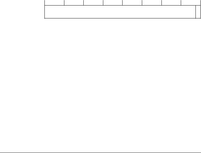
Figure 3-50 on page 3-91 shows the bit arrangement for the Data TCM Region Register.
ARM DDI 0333H |
Copyright © 2004-2009 ARM Limited. All rights reserved. |
3-90 |
ID012410 |
Non-Confidential, Unrestricted Access |
|
System Control Coprocessor
31 |
12 11 |
7 |
6 |
2 |
1 |
0 |
|
Base address (physical address) |
|
|
SBZ/UNP |
|
Size |
S |
E |
|
|
|
B |
||||
|
|
|
|
|
|
Z |
n |
Figure 3-50 Data TCM Region Register format
Table 3-85 lists how the bit values correspond with the Data TCM Region Register functions.
|
|
|
Table 3-85 Data TCM Region Register bit functions |
|
|
|
|
Bits |
Field name |
Function |
|
|
|
|
|
[31:12] |
Base address |
Contains the physical base address of the TCM. |
|
|
|
The base address must be aligned to the size of the TCM. |
|
|
|
Any bits in the range [(log2(RAMSize)-1):12] are ignored. The base address is 0 at Reset. |
|
|
|
|
|
[11:7] |
- |
UNP/SBZ. |
|
|
|
|
|
[6:2] |
Size |
Indicates the size of the TCM on readsa. All other values are reserved: |
|
|
|
b00000 |
= 0KB |
|
|
b00011 |
= 4KB |
|
|
b00100 |
= 8KB |
|
|
b00101 |
= 16KB |
|
|
b00110 |
= 32KB. |
|
|
|
|
[1] |
- |
UNP/SBZ. |
|
|
|
|
|
[0] |
En |
Indicates if the TCM is enabled. |
|
|
|
0 = TCM disabled, reset value |
|
|
|
1 = TCM enabled. |
a. On writes this field is ignored. For more details see Tightly-coupled memory on page 7-7.
Attempts to write to this register in Secure Privileged mode when CP15SDISABLE is HIGH result in an Undefined exception, see TrustZone write access disable on page 2-9.
Note
When the NS access bit is 0 for Data TCM, see c9, Data TCM Non-secure Control Access Register on page 3-94, attempts to access the Data TCM Region Register from the Non-secure world cause an Undefined exception.
Table 3-86 lists the results of attempted access for each mode.
Table 3-86 Results of access to the Data TCM Region Register
NS access bit value |
Secure Privileged |
Non-secure Privileged |
User |
|||
Read |
Write |
Read |
Write |
|||
|
|
|||||
|
|
|
|
|
|
|
0 |
Data |
Data |
Undefined exception |
|
|
|
|
|
|
|
|
1 |
Data |
Data |
Data |
Data |
Undefined exception |
|
|
|
|
|
|
|
To use the Data TCM Region Register read or write CP15 with:
•Opcode_1 set to 0
•CRn set to c9
ARM DDI 0333H |
Copyright © 2004-2009 ARM Limited. All rights reserved. |
3-91 |
ID012410 |
Non-Confidential, Unrestricted Access |
|
System Control Coprocessor
•CRm set to c1
•Opcode_2 set to 0.
For example:
MRC |
p15, |
0, |
<Rd>, |
c9, |
c1, |
0 |
; |
Read Data TCM Region Register |
MCR |
p15, |
0, |
<Rd>, |
c9, |
c1, |
0 |
; |
Write Data TCM Region Register |
Attempting to change the Data TCM Region Register while a DMA operation is running has Unpredictable effects but there is no impact on security.
3.2.26c9, Instruction TCM Region Register
The purpose of the Instruction TCM Region Register is to describe the physical base address and size of the Instruction TCM region and to provide a mechanism to enable it.
Table 3-87 lists the purposes of the individuals bits of the Instruction TCM Region Register.
The Instruction TCM Region Register is:
•in CP15 c9
•a 32-bit read/write register common to Secure and Non-secure worlds
•accessible in privileged modes only.
If the processor is configured to have 2 Instruction TCMs, each TCM has a separate Instruction TCM Region Register. The TCM Selection Register determines the register in use.
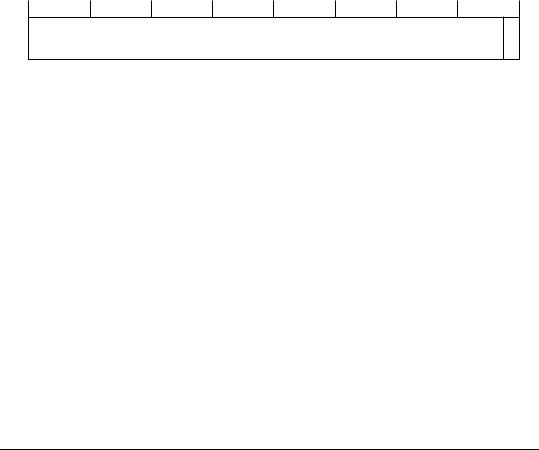
Figure 3-51 shows the bit arrangement for the Instruction TCM Region Register.
31 |
12 11 |
7 |
6 |
2 |
1 |
0 |
|
Base address (physical address) |
|
|
SBZ/UNP |
|
Size |
S |
E |
|
|
|
B |
||||
|
|
|
|
|
|
Z |
n |
Figure 3-51 Instruction TCM Region Register format
Table 3-87 lists how the bit values correspond with the Instruction TCM Region Register functions.
|
|
Table 3-87 Instruction TCM Region Register bit functions |
|
|
|
|
|
Bits |
Field |
Function |
|
name |
|||
|
|
||
|
|
|
|
[31:12] |
Base |
Contains the physical base address of the TCM. The base address must be aligned to the size of the |
|
|
address |
TCM. Any bits in the range [(log2(RAMSize)-1):12] are ignored. |
|
|
|
The base address is 0 at Reset. |
|
|
|
|
|
[11:7] |
- |
UNP/SBZ. |
ARM DDI 0333H |
Copyright © 2004-2009 ARM Limited. All rights reserved. |
3-92 |
ID012410 |
Non-Confidential, Unrestricted Access |
|
System Control Coprocessor
|
|
|
Table 3-87 Instruction TCM Region Register bit functions (continued) |
|
|
|
|
|
|
Bits |
Field |
Function |
||
name |
||||
|
|
|
||
|
|
|
||
[6:2] |
Size |
Indicates the size of the TCM on readsa. All other values are reserved: |
||
|
|
b00000 |
= 0KB |
|
|
|
b00011 |
= 4KB |
|
|
|
b00100 |
= 8KB |
|
|
|
b00101 |
= 16KB |
|
|
|
b00110 |
= 32KB. |
|
|
|
|
||
[1] |
- |
UNP/SBZ. |
||
|
|
|
||
[0] |
En |
Indicates if the TCM is enabled: |
||
|
|
0 = TCM disabled. |
1 = TCM enabled.
The reset value of this bit depends on the value of the INITRAM static configuration signal. If INITRAM is HIGH then this bit resets to 1. If INITRAM is LOW then this bit resets to 0. For more information see Static configuration signals on page A-4.
a. On writes this field is ignored. For more details see Tightly-coupled memory on page 7-7.
Attempts to write to this register in Secure Privileged mode when CP15SDISABLE is HIGH result in an Undefined exception, see TrustZone write access disable on page 2-9.
The value of the En bit at Reset depends on the INITRAM signal:
•INITRAM LOW sets En to 0
•INITRAM HIGH sets En to 1.
When INITRAM is HIGH this enables the Instruction TCM directly from reset, with a Base address of 0x00000. When the processor comes out of reset, it executes the instructions in the Instruction TCM instead of fetching instructions from external memory, except when the processor uses high vectors.
Note
When the NS access bit is 0 for Instruction TCM, see c9, Instruction TCM Non-secure Control Access Register on page 3-95, attempts to access the Instruction TCM Region Register from the Non-secure world cause an Undefined exception.
Table 3-88 lists the results of attempted access for each mode.
Table 3-88 Results of access to the Instruction TCM Region Register
NS access bit value |
Secure Privileged |
Non-secure Privileged |
User |
|||
Read |
Write |
Read |
Write |
|||
|
|
|||||
|
|
|
|
|
|
|
0 |
Data |
Data |
Undefined exception |
|
|
|
|
|
|
|
|
1 |
Data |
Data |
Data |
Data |
Undefined exception |
|
|
|
|
|
|
|
To use the Instruction TCM Region Register read or write CP15 with:
•Opcode_1 set to 0
•CRn set to c9
•CRm set to c1
ARM DDI 0333H |
Copyright © 2004-2009 ARM Limited. All rights reserved. |
3-93 |
ID012410 |
Non-Confidential, Unrestricted Access |
|
System Control Coprocessor
• Opcode_2 set to 1. For example:
MRC p15, 0, <Rd>, c9, c1, 1 ; Read Instruction TCM Region Register
MCR p15, 0, <Rd>, c9, c1, 1 ; Write Instruction TCM Region Register
Attempts to change the Instruction TCM Region Register while a DMA operation is running has Unpredictable effects but there is no impact on security.
3.2.27c9, Data TCM Non-secure Control Access Register
The purpose of the Data TCM Non-secure Access Register is to:
•set access permission to the Data TCM Region Register
•define data in the Data TCM as Secure or Non-secure.
The Data TCM Non-secure Control Access Register is:
•in CP15 c9
•a 32-bit read/write register in the Secure world only
•accessible in privileged modes only.
If the processor is configured to have 2 Data TCMs, each TCM has a separate Data TCM Non-secure Control Access Register. The TCM Selection Register determines the register in use.
Figure 3-52 shows the bit arrangement for the Data TCM Non-secure Control Access Register.
31 |
1 |
0 |
SBZ
NS access
Figure 3-52 Data TCM Non-secure Control Access Register format
Table 3-89 lists how the bit values correspond with the register functions.
|
|
Table 3-89 Data TCM Non-secure Control Access Register bit functions |
|
|
|
|
|
Bits |
Field |
Function |
|
name |
|||
|
|
||
|
|
|
|
[31:1] |
- |
UNP/SBZ. |
|
|
|
|
|
[0] |
NS access |
Makes Data TCM invisible to the Non-secure world and makes TCM data Secure. |
|
|
|
0 = Data TCM Region Register only accessible in the Secure world. Data TCM only visible in the |
|
|
|
Secure world and only when the NS Attribute in the page table is 0. The reset value is 0. |
|
|
|
1 = Data TCM Region Register accessible in the Secure and Non-secure worlds. Data TCM is |
|
|
|
visible in the Non-secure world, and also in the Secure world if the NS Attribute in the page table |
|
|
|
is 1. |
|
|
|
|
ARM DDI 0333H |
Copyright © 2004-2009 ARM Limited. All rights reserved. |
3-94 |
ID012410 |
Non-Confidential, Unrestricted Access |
|
System Control Coprocessor
Table 3-90 lists the effect on TCM operations for different combinations of operating world and NS bits.
Table 3-90 Effects of NS items for data TCM operation
World |
NS |
NS page |
Region |
Control |
Data |
|
acces |
||||||
table |
visible |
|||||
|
s |
|
|
|||
|
|
|
|
|
||
|
|
|
|
|
|
|
Secure |
0 |
1 |
No |
- |
- |
|
|
|
|
|
|
|
|
|
1 |
0 |
No |
- |
- |
|
|
|
|
|
|
|
|
|
0 |
0 |
Yes |
Secure privileged only |
Secure only |
|
|
|
|
|
|
|
|
|
1 |
1 |
Yes |
Secure and Non-secure privileged |
Non-secure only |
|
|
|
|
|
|
|
|
Non-secure |
1 |
X |
Yes |
Secure and Non-secure privileged |
Non-secure only |
|
|
|
|
|
|
|
|
|
0 |
X |
No |
- |
- |
|
|
|
|
|
|
|
Attempts to write to this register in Secure Privileged mode when CP15SDISABLE is HIGH result in an Undefined exception, see TrustZone write access disable on page 2-9.
Attempts to access the Data TCM Non-secure Control Access Register in modes other than
Secure privileged result in an Undefined exception.
To use the Data TCM Non-secure Control Access Register read or write CP15 with:
•Opcode_1 set to 0
•CRn set to c9
•CRm set to c1
•Opcode_2 set to 2.
For example:
MRC |
p15,0,<Rd>,c9,c1,2 |
; |
Read Data TCM Non-secure Control Access Register |
MCR |
p15,0,<Rd>,c9,c1,2 |
; |
Write Data TCM Non-secure Control Access Register |
3.2.28c9, Instruction TCM Non-secure Control Access Register
The purpose of the Instruction TCM Non-secure Control Access Register is to:
•set access permission to the Instruction TCM Region Register
•define instructions in the Instruction TCM as Secure or Non-secure.
The Instruction TCM Non-secure Control Access Register is:
•in CP15 c9
•a 32-bit read/write register in the Secure world only
•accessible in privileged modes only.
If the processor is configured to have 2 Instruction TCMs, each TCM has a separate Instruction TCM Non-secure Control Access Register. The TCM Selection Register determines the register in use.
Figure 3-53 on page 3-96 shows the bit arrangement for the Instruction TCM Non-secure
Control Access Register.
ARM DDI 0333H |
Copyright © 2004-2009 ARM Limited. All rights reserved. |
3-95 |
ID012410 |
Non-Confidential, Unrestricted Access |
|
System Control Coprocessor
31 |
1 |
0 |
SBZ
NS access
Figure 3-53 Instruction TCM Non-secure Control Access Register format
Table 3-91 lists how the bit values correspond with the register functions.
|
|
Table 3-91 Instruction TCM Non-secure Control Access Register bit functions |
|
|
|
|
|
Bits |
Field |
Function |
|
name |
|||
|
|
||
|
|
|
|
[31:1] |
- |
UNP/SBZ. |
|
|
|
|
|
[0] |
NS access |
Makes Instruction TCM invisible to the Non-secure world and makes TCM data Secure. |
|
|
|
0 = Instruction TCM Region Register only accessible in the Secure world. Instruction TCM only |
|
|
|
visible in the Secure world and only when the NS Attribute in the page table is 0. The reset value |
|
|
|
is 0. |
|
|
|
1 = Instruction TCM Region Register accessible in the Secure and Non-secure worlds. Instruction |
|
|
|
TCM is visible in the Non-secure world, and also in the Secure world if the NS Attribute in the |
|
|
|
page table is 1. |
|
|
|
|
Table 3-92 lists the effect on TCM operations for different combinations of operating world, and NS bits.
Table 3-92 Effects of NS items for instruction TCM operation
World |
NS |
NS page |
Region |
Control |
Data |
|
access |
table |
visible |
||||
|
|
|
||||
|
|
|
|
|
|
|
Secure |
0 |
1 |
No |
- |
- |
|
|
|
|
|
|
|
|
|
1 |
0 |
No |
- |
- |
|
|
|
|
|
|
|
|
|
0 |
0 |
Yes |
Secure privileged only |
Secure only |
|
|
|
|
|
|
|
|
|
1 |
1 |
Yes |
Secure and Non-secure privileged |
Non-secure only |
|
|
|
|
|
|
|
|
Non-secure |
1 |
X |
Yes |
Secure and Non-secure privileged |
Non-secure only |
|
|
|
|
|
|
|
|
|
0 |
X |
No |
- |
- |
|
|
|
|
|
|
|
Attempts to write to this register in Secure Privileged mode when CP15SDISABLE is HIGH result in an Undefined exception, see TrustZone write access disable on page 2-9.
Attempts to access the Instruction TCM Non-secure Control Access Register in modes other than Secure Privileged result in an Undefined exception.
To use the Instruction TCM Non-secure Control Access Register read or write CP15 with:
•Opcode_1 set to 0
•CRn set to c9
•CRm set to c1
•Opcode_2 set to 3.
For example:
|
MRC p15,0,<Rd>,c9,c1,3 |
;Read Instruction TCM Non-secure Control Access Register |
|
|
|
|
|
ARM DDI 0333H |
Copyright © 2004-2009 ARM Limited. All rights reserved. |
3-96 |
|
ID012410 |
Non-Confidential, Unrestricted Access |
|