


System Control Coprocessor
Some of the functionality depends on how you set external signals at reset.
System control and configuration behaves in three ways:
•as a set of flags or enables for specific functionality
•as a set of numbers, values that indicate system functionality
•as a set of addresses for processes in memory.
3.1.3MMU control and configuration
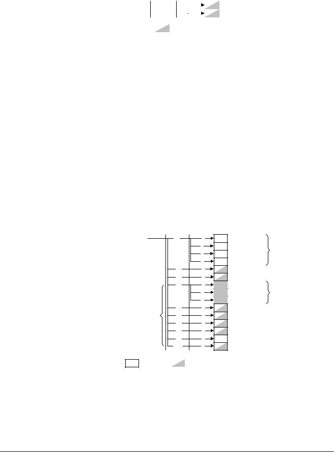
The purpose of the MMU control and configuration registers is to:
•allocate physical address locations from the Virtual Addresses (VAs) that the processor generates.
•control program access to memory.
•designate areas of memory as either:
—Noncacheable
—unbufferable
—Noncacheable and unbufferable.
•detect MMU faults and external aborts
•hold thread and process IDs
•provide direct access to the TLB lockdown entries.
The MMU control and configuration registers consist of one 32-bit read-only register, one 32-bit write-only register, and 22 32-bit read/write registers. Figure 3-2 on page 3-7 shows the arrangement of registers in this functional group.
ARM DDI 0333H |
Copyright © 2004-2009 ARM Limited. All rights reserved. |
3-6 |
ID012410 |
Non-Confidential, Unrestricted Access |
|

System Control Coprocessor
CRn |
Opcode_1 CRm Opcode_2 |
c0 |
0 |
c0 |
3 |
c2 |
0 |
c0 |
0 |
|
|
|
1 |
|
|
|
2 |
c3 |
0 |
c0 |
0 |
c5 |
0 |
c0 |
0 |
|
|
|
1 |
c6 |
0 |
c0 |
0 |
|
|
|
1 |
|
|
|
2 |
c8 |
0 |
|
|
c10 |
0 |
c0 |
|
|
|
c2 |
0 |
|
|
|
1 |
c13 |
0 |
c0 |
0 |
|
|
|
1 |
|
|
|
2 |
|
|
|
3 |
|
|
|
4 |
c15 |
0 |
c2 |
4 |
|
5 |
c4 |
2 |
|
|
c5 |
2 |
|
|
c6 |
2 |
|
|
c7 |
2 |
TLB Type Register |
|
|
Translation Table Base Register 0 |
|
|
Translation Table Base Register 1 |
|
|
Translation Table Base Control Register |
|
|
Domain Access Control Register |
|
|
Data Fault Status Register |
|
|
Instruction Fault Status Register |
|
|
Fault Address Register |
|
|
Watchpoint Fault Address Register |
|
|
Instruction Fault Address Register |
|
|
TLB Operations Register |
|
|
TLB Lockdown Register |
|
|
Primary Region Remap Register |
Memory region |
|
Normal Memory Remap Register |
remap registers |
|
FCSE PID Register |
|
|
Context ID Register |
|
|
User Read/Write Thread and Process ID Register |
Thread and |
|
User Read Only Thread and Process ID Register |
process ID |
|
Privileged Only Thread and Process ID Register |
registers |
|
Peripheral Port Memory Remap Register |
|
|
TLB Lockdown Index Register |
|
|
TLB Lockdown VA Register |
TLB lockdown |
|
TLB Lockdown PA Register |
access registers |
|
TLB Lockdown Attributes Register |
|
|
Read-only |
|
Read/write |
|
Write-only Accessible in User mode |
Figure 3-2 MMU control and configuration registers
To use the MMU control and configuration registers you read or write individual registers that make up the group, see Use of the system control coprocessor on page 3-12.
MMU control and configuration behaves in three ways:
•as a set of numbers, values that describe aspects of the MMU or indicate its current state
•as a set of addresses for tables in memory
•as a set of operations that act on the MMU.
3.1.4Cache control and configuration
The purpose of the cache control and configuration registers is to:
•provide information on the size and architecture of the instruction and data caches
•control instruction and data cache lockdown
•control cache maintenance operations that include clean and invalidate caches, drain and flush buffers, and address translation
•override cache behavior during debug or interruptible cache operations.
The cache control and configuration registers consist of one 32-bit read only register and four 32-bit read/write registers. Figure 3-3 on page 3-8 shows the arrangement of the registers in this functional group.
ARM DDI 0333H |
Copyright © 2004-2009 ARM Limited. All rights reserved. |
3-7 |
ID012410 |
Non-Confidential, Unrestricted Access |
|

|
|
|
|
|
|
|
|
|
|
|
|
|
|
|
|
|
|
|
|
|
|
|
|
|
System Control Coprocessor |
CRn |
|
Opcode_1 |
CRm |
|
Opcode_2 |
|
|
||||||||||||||||||
c0 |
|
|
|
|
|
|
|
|
|
|
|
|
|
|
|
|
|
Cache Type Register |
|||||||
|
|
0 |
|
|
|
c0 |
|
|
|
1 |
|
|
|
|
|||||||||||
|
|
|
|
|
|
|
|
|
|
|
|
||||||||||||||
c7 |
|
|
|
|
|
|
|
|
|
|
|
|
|
|
|
|
|
|
|
|
|
|
|
|
Cache Operations Register |
|
|
|
|
0 |
|
|
|
|
|
|
|
|
|
|
|
|
|
|
|
|
|
|
|
||
|
|
|
|
|
|
|
|
|
|
|
|
|
|
|
|
|
|
|
|
|
|||||
c9 |
|
|
|
|
|
|
|
|
|
|
|
|
|
|
|
|
|
|
|
|
|
|
|
Data Cache Lockdown Register |
|
|
|
|
0 |
|
|
|
|
|
c0 |
|
|
|
|
|
0 |
|
|
|
|
||||||
|
|
|
|
|
|
|
|
|
|
|
|
|
|
||||||||||||
|
|
|
|
|
|
|
|
|
|
|
|
|
|
|
|
|
|
|
|
|
|
|
|
Instruction Cache Lockdown Register |
|
|
|
|
|
|
|
|
|
|
|
|
|
|
|
|
|
|
|
|
1 |
|
|
|
|
||
|
|
|
|
|
|
|
|
|
|
|
|
|
|
|
|
|
|
|
|
|
|
||||
|
|
|
|
|
|
|
|
|
|
|
|
|
|
|
|
|
|
Cache Behavior Override Register |
|||||||
|
|
|
|
|
|
|
|
|
|
|
c8 |
|
|
|
|
|
|
0 |
|
|
|
||||
|
|
|
|
|
|
|
|
|
|
|
|
|
|
|
|
||||||||||
|
|
|
|
Read-only |
|
|
|
|
|
|
|
Read/write |
|
Write only Accessible in User mode |
|||||||||||
|
|
|
|
|
|
|
|
|
|
|
|
||||||||||||||
|
|
|
|
|
|
|
|
|
|
|
|
||||||||||||||
|
|
|
|
|
|
|
|
|
|
|
|
||||||||||||||
Figure 3-3 Cache control and configuration registers
To use the system control and configuration registers you read or write individual registers that make up the group, see Use of the system control coprocessor on page 3-12.
Cache control and configuration registers behave as:
•a set of numbers, values that describe aspects of the caches
•a set of bits that enable specific cache functionality
•a set of operations that act on the caches.
3.1.5TCM control and configuration
The purpose of the TCM control and configuration registers is to:
•inform the processor about the status of the TCM regions
•define TCM regions.
The TCM control and configuration registers consist of one 32-bit read-only register and five 32-bit read/write registers. Figure 3-4 shows the arrangement of registers.
CRn |
|
Opcode_1 |
CRm |
Opcode_2 |
|
|
||||||||||||||||||||
c0 |
|
|
0 |
|
|
|
|
c0 |
|
|
|
|
|
2 |
|
|
|
|
|
|
|
|
TCM Status Register |
|||
|
|
|
|
|
|
|
|
|
|
|
|
|
|
|||||||||||||
c9 |
|
|
|
|
|
|
|
|
|
|
|
|
|
|
|
|
|
|
|
|
|
|
|
|
|
Data TCM Region Register |
|
|
|
|
|
|
|
|
|
|
|
|
|
|
|
|
|
|
|
|
|
|
|||||
|
|
|
0 |
|
|
|
|
c1 |
|
|
|
|
0 |
|
|
|
|
|
|
|
||||||
|
|
|
|
|
|
|
|
|
|
|
|
|
|
|
|
|||||||||||
|
|
|
|
|
|
|
|
|
|
|
|
|
|
|
|
|
|
|
|
|
|
|
|
|
|
Instruction TCM Region Register |
|
|
|
|
|
|
|
|
|
|
|
|
|
|
|
|
|
1 |
|
|
|
|
|
|
|||
|
|
|
|
|
|
|
|
|
|
|
|
|
|
|
|
|
|
|
|
|
|
|||||
|
|
|
|
|
|
|
|
|
|
|
|
|
|
|
|
|
|
|
|
|
|
|
|
Data TCM Non-secure Access Control Register |
||
|
|
|
|
|
|
|
|
|
|
|
|
|
|
|
|
|
2 |
|
|
|
|
|
|
|||
|
|
|
|
|
|
|
|
|
|
|
|
|
|
|
|
|
|
|
|
|
||||||
|
|
|
|
|
|
|
|
|
|
|
|
|
|
|
|
|
|
|
|
|
|
|
|
|
|
Instruction TCM Non-secure Access Control Register |
|
|
|
|
|
|
|
|
|
|
|
|
|
|
|
|
|
3 |
|
|
|
|
|
|
|||
|
|
|
|
|
|
|
|
|
|
|
|
|
|
|
|
|
|
|
|
|
||||||
|
|
|
|
|
|
|
|
|
|
|
|
|
|
|
|
|
|
|
|
|
|
|
|
|
|
TCM Selection Register |
|
|
|
|
|
|
|
|
|
c2 |
|
|
|
|
|
0 |
|
|
|
|
|
|
|
||||
|
|
|
|
|
|
|
|
|
|
|
|
|
|
|
|
|
||||||||||
|
|
|
Read-only |
|
|
|
|
|
|
Read/write |
|
Write-only Accessible in User mode |
||||||||||||||
|
|
|
|
|
|
|
|
|
|
|||||||||||||||||
|
|
|
|
|
|
|
|
|
|
|||||||||||||||||
Figure 3-4 TCM control and configuration registers
To use the system control and configuration registers you read or write individual registers that make up the group, see Use of the system control coprocessor on page 3-12.
TCM control and configuration behaves in three ways:
•as a set of numbers, values that describe aspects of the TCMs
•as a set of bits that enable specific TCM functionality
•as a set of addresses that define the memory locations of data stored in the TCMs.
3.1.6Cache Master Valid Registers
The purpose of the Cache Master Valid Registers is to hold the state of the Master Valid bits of the instruction and data caches.
The cache debug registers consist of two 32-bit read/write registers. Figure 3-5 on page 3-9 shows the arrangement of registers in this functional group.
ARM DDI 0333H |
Copyright © 2004-2009 ARM Limited. All rights reserved. |
3-8 |
ID012410 |
Non-Confidential, Unrestricted Access |
|
|
|
|
|
|
|
|
|
|
|
|
|
|
|
System Control Coprocessor |
CRn |
|
Opcode_1 |
|
CRm |
Opcode_2 |
|
|
|||||||
c15 |
|
|
3 |
|
|
|
|
c8 |
|
|
|
|
|
Instruction Cache Master Valid Register |
|
|
|
|
|
|
|
|
|
|
|
||||
|
|
|
|
|
|
|
|
|
|
|
|
|
|
Data Cache Master Valid Register |
|
|
|
|
|
|
|
c12 |
|
|
|
|
|||
|
|
|
|
|
|
|
|
|
|
|
||||
|
|
Read-only |
|
|
|
|
|
|
Read/write |
|
Write-only Accessible in User mode |
|||
|
|
|
|
|
|
|
|
|
||||||
|
|
|
|
|
|
|
|
|
||||||
|
|
|
|
|
|
|
|
|
|
|
|
|
Figure 3-5 Cache Master Valid Registers |
|
To use the Cache Master Valid Registers you read or write the individual registers that make up the group, see Use of the system control coprocessor on page 3-12.
The Cache Master Valid Registers behave as a set of bits that define the cache contents as valid or invalid. The number of bits is a function of the cache size.
3.1.7DMA control
The purpose of the DMA control registers is to:
•enable software to control DMA
•transfer large blocks of data between the TCM and an external memory
•determine accessibility
•select DMA channel.
The Enable, Control, Internal Start Address, External Start Address, Internal End Address, Channel Status, and Context ID Registers are multiple registers with one register of each for each channel that is implemented.
The DMA control registers consist of five 32-bit read-only registers, three 32-bit write-only registers and seven 32-bit read/write registers. Figure 3-6 shows the arrangement of registers.
CRn Opcode_1
c11 |
|
0 |
|
One register per channel selected by DMA Channel Number Register
CRm |
Opcode_2 |
|
|
c0 |
0 |
Present |
DMA Identification |
|
1 |
Queued |
|
|
2 |
Running |
and Status Registers |
|
3 |
Interrupting |
|
c1 |
0 |
DMA User Accessibility Register |
|
c2 |
0 |
DMA Channel Number Register |
|
c3 |
0 |
Stop |
DMA Enable |
|
1 |
Start |
|
|
Registers |
||
|
2 |
Clear |
|
|
|
||
c4 |
0 |
DMA Control Register |
|
c5 |
0 |
DMA Internal Start Address Register |
|
c6 |
0 |
DMA External Start Address Register |
|
c7 |
0 |
DMA Internal End Address Register |
|
c8 |
0 |
DMA Channel Status Register |
|
c15 |
0 |
DMA Context ID Register |
|
Read-only |
|
Read/write |
|
Write-only Accessible in User mode |
Figure 3-6 DMA control and configuration registers
To use the DMA control and configuration registers you read or write the individual registers that make up the group, see Use of the system control coprocessor on page 3-12.
Code can execute several DMA operations while in User mode if these operations are enabled by the DMA User Accessibility Register.
ARM DDI 0333H |
Copyright © 2004-2009 ARM Limited. All rights reserved. |
3-9 |
ID012410 |
Non-Confidential, Unrestricted Access |
|