

- •Features
- •Pin Configurations
- •Disclaimer
- •Overview
- •Block Diagram
- •Pin Descriptions
- •Port A (PA7..PA0)
- •Port B (PB7..PB0)
- •Port C (PC7..PC0)
- •Port D (PD7..PD0)
- •RESET
- •XTAL1
- •XTAL2
- •AVCC
- •AREF
- •AVR CPU Core
- •Introduction
- •Architectural Overview
- •Status Register
- •Stack Pointer
- •Interrupt Response Time
- •SRAM Data Memory
- •Data Memory Access Times
- •EEPROM Data Memory
- •EEPROM Read/Write Access
- •I/O Memory
- •Clock Systems and their Distribution
- •CPU Clock – clkCPU
- •I/O Clock – clkI/O
- •Flash Clock – clkFLASH
- •ADC Clock – clkADC
- •Clock Sources
- •Default Clock Source
- •Crystal Oscillator
- •External RC Oscillator
- •External Clock
- •Timer/Counter Oscillator
- •Idle Mode
- •Power-down Mode
- •Power-save Mode
- •Standby Mode
- •Extended Standby Mode
- •Analog to Digital Converter
- •Analog Comparator
- •Brown-out Detector
- •Internal Voltage Reference
- •Watchdog Timer
- •Port Pins
- •Resetting the AVR
- •Reset Sources
- •Power-on Reset
- •External Reset
- •Brown-out Detection
- •Watchdog Reset
- •Watchdog Timer
- •Interrupts
- •I/O Ports
- •Introduction
- •Configuring the Pin
- •Reading the Pin Value
- •Unconnected pins
- •Alternate Port Functions
- •Alternate Functions of Port A
- •Alternate Functions of Port B
- •Alternate Functions of Port C
- •Alternate Functions of Port D
- •Port A Data Register – PORTA
- •Port B Data Register – PORTB
- •Port C Data Register – PORTC
- •Port D Data Register – PORTD
- •External Interrupts
- •8-bit Timer/Counter0 with PWM
- •Overview
- •Registers
- •Definitions
- •Counter Unit
- •Output Compare Unit
- •Force Output Compare
- •Modes of Operation
- •Normal Mode
- •Fast PWM Mode
- •Phase Correct PWM Mode
- •Internal Clock Source
- •Prescaler Reset
- •External Clock Source
- •16-bit Timer/Counter1
- •Overview
- •Registers
- •Definitions
- •Compatibility
- •Counter Unit
- •Input Capture Unit
- •Input Capture Trigger Source
- •Noise Canceler
- •Using the Input Capture Unit
- •Output Compare Units
- •Force Output Compare
- •Modes of Operation
- •Normal Mode
- •Fast PWM Mode
- •Phase Correct PWM Mode
- •8-bit Timer/Counter2 with PWM and Asynchronous Operation
- •Overview
- •Registers
- •Definitions
- •Counter Unit
- •Output Compare Unit
- •Force Output Compare
- •Modes of Operation
- •Normal Mode
- •Fast PWM Mode
- •Phase Correct PWM Mode
- •Timer/Counter Prescaler
- •SS Pin Functionality
- •Slave Mode
- •Master Mode
- •SPI Control Register – SPCR
- •SPI Status Register – SPSR
- •SPI Data Register – SPDR
- •Data Modes
- •USART
- •Overview
- •AVR USART vs. AVR UART – Compatibility
- •Clock Generation
- •External Clock
- •Synchronous Clock Operation
- •Frame Formats
- •Parity Bit Calculation
- •USART Initialization
- •Parity Generator
- •Disabling the Transmitter
- •Receiver Error Flags
- •Parity Checker
- •Disabling the Receiver
- •Flushing the Receive Buffer
- •Asynchronous Data Recovery
- •Using MPCM
- •Write Access
- •Read Access
- •Two-wire Serial Interface
- •Features
- •TWI Terminology
- •Electrical Interconnection
- •Transferring Bits
- •START and STOP Conditions
- •Address Packet Format
- •Data Packet Format
- •Overview of the TWI Module
- •SCL and SDA Pins
- •Bit Rate Generator Unit
- •Bus Interface Unit
- •Address Match Unit
- •Control Unit
- •TWI Register Description
- •TWI Bit Rate Register – TWBR
- •TWI Control Register – TWCR
- •TWI Status Register – TWSR
- •TWI Data Register – TWDR
- •Using the TWI
- •Transmission Modes
- •Master Transmitter Mode
- •Master Receiver Mode
- •Slave Receiver Mode
- •Slave Transmitter Mode
- •Miscellaneous States
- •Analog Comparator
- •Analog Comparator Multiplexed Input
- •Features
- •Operation
- •Starting a Conversion
- •Differential Gain Channels
- •Changing Channel or Reference Selection
- •ADC Input Channels
- •ADC Voltage Reference
- •ADC Noise Canceler
- •Analog Input Circuitry
- •ADC Accuracy Definitions
- •ADC Conversion Result
- •ADLAR = 0
- •ADLAR = 1
- •Features
- •Overview
- •Test Access Port – TAP
- •TAP Controller
- •PRIVATE0; $8
- •PRIVATE1; $9
- •PRIVATE2; $A
- •PRIVATE3; $B
- •Bibliography
- •Features
- •System Overview
- •Data Registers
- •Bypass Register
- •Device Identification Register
- •Reset Register
- •Boundary-scan Chain
- •EXTEST; $0
- •IDCODE; $1
- •SAMPLE_PRELOAD; $2
- •AVR_RESET; $C
- •BYPASS; $F
- •Scanning the Digital Port Pins
- •Scanning the RESET Pin
- •Scanning the Clock Pins
- •Scanning the ADC
- •Features
- •Application Section
- •BLS – Boot Loader Section
- •Read-While-Write and no Read-While-Write Flash Sections
- •Boot Loader Lock Bits
- •Performing a Page Write
- •Using the SPM Interrupt
- •Setting the Boot Loader Lock Bits by SPM
- •Reading the Fuse and Lock Bits from Software
- •Preventing Flash Corruption
- •Fuse Bits
- •Latching of Fuses
- •Signature Bytes
- •Calibration Byte
- •Signal Names
- •Parallel Programming
- •Enter Programming Mode
- •Chip Erase
- •Programming the Flash
- •Programming the EEPROM
- •Reading the Flash
- •Reading the EEPROM
- •Programming the Lock Bits
- •Reading the Signature Bytes
- •Reading the Calibration Byte
- •SPI Serial Downloading
- •Data Polling Flash
- •Data Polling EEPROM
- •AVR_RESET ($C)
- •PROG_ENABLE ($4)
- •PROG_COMMANDS ($5)
- •PROG_PAGELOAD ($6)
- •PROG_PAGEREAD ($7)
- •Data Registers
- •Reset Register
- •Programming Enable Register
- •Virtual Flash Page Read Register
- •Programming Algorithm
- •Entering Programming Mode
- •Leaving Programming Mode
- •Performing Chip Erase
- •Programming the Flash
- •Reading the Flash
- •Programming the EEPROM
- •Reading the EEPROM
- •Programming the Fuses
- •Programming the Lock Bits
- •Reading the Signature Bytes
- •Reading the Calibration Byte
- •Electrical Characteristics
- •Absolute Maximum Ratings*
- •DC Characteristics
- •External Clock Drive Waveforms
- •External Clock Drive
- •Two-wire Serial Interface Characteristics
- •ADC Characteristics
- •Register Summary
- •Instruction Set Summary
- •Ordering Information
- •Packaging Information
- •Errata
- •ATmega32 Rev. A
- •Datasheet Change Log for ATmega32
- •Changes from Rev. 2503E-09/03 to Rev. 2503F-12/03
- •Changes from Rev. 2503D-02/03 to Rev. 2503E-09/03
- •Changes from Rev. 2503C-10/02 to Rev. 2503D-02/03
- •Changes from Rev. 2503B-10/02 to Rev. 2503C-10/02
- •Changes from Rev. 2503A-03/02 to Rev. 2503B-10/02
- •Table of Contents

Ordering Information
Speed (MHz) |
Power Supply |
Ordering Code |
Package |
Operation Range |
|
|
|
|
|
8 |
2.7 - 5.5V |
ATmega32L-8AC |
44A |
Commercial |
|
|
ATmega32L-8PC |
40P6 |
(0oC to 70oC) |
|
|
ATmega32L-8MC |
44M1 |
|
|
|
|
|
|
|
|
ATmega32L-8AI |
44A |
Industrial |
|
|
ATmega32L-8PI |
40P6 |
(-40oC to 85oC) |
|
|
ATmega32L-8MI |
44M1 |
|
|
|
|
|
|
16 |
4.5 - 5.5V |
ATmega32-16AC |
44A |
Commercial |
|
|
ATmega32-16PC |
40P6 |
(0oC to 70oC) |
|
|
ATmega32-16MI |
44M1 |
|
|
|
|
|
|
|
|
ATmega32-16AI |
44A |
Industrial |
|
|
ATmega32-16PI |
40P6 |
(-40oC to 85oC) |
|
|
ATmega32-16MC |
44M1 |
|
|
|
|
|
|
|
Package Type |
|
|
44A |
44-lead, Thin (1.0 mm) Plastic Gull Wing Quad Flat Package (TQFP) |
|
|
40P6 |
40-pin, 0.600” Wide, Plastic Dual Inline Package (PDIP) |
|
|
44M1 |
44-pad, 7 x 7 x 1.0 mm body, lead pitch 0.50 mm, Micro Lead Frame Package (MLF) |
|
|
304 ATmega32(L)
2503F–AVR–12/03
ATmega32(L)
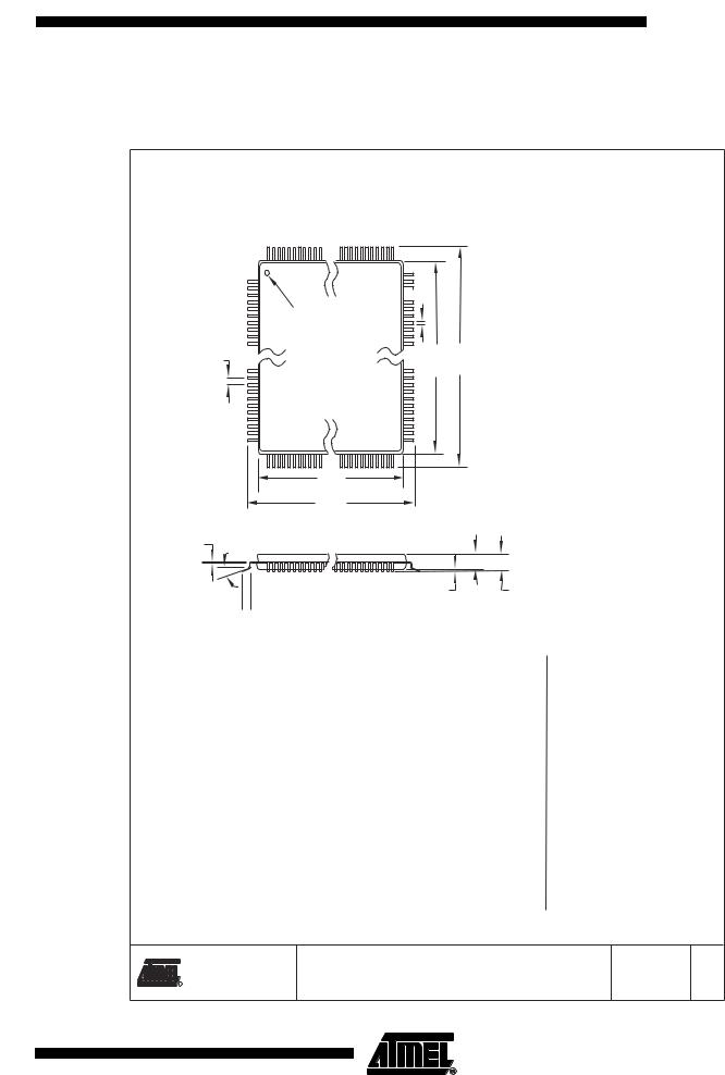
Packaging Information
44A
PIN 1 
 B
B
PIN 1 IDENTIFIER
e |
E1 E |
D1
D
C |
0˚~7˚ |
A1 A2

 L
L
Notes: 1. This package conforms to JEDEC reference MS-026, Variation ACB.
2.Dimensions D1 and E1 do not include mold protrusion. Allowable protrusion is 0.25 mm per side. Dimensions D1 and E1 are maximum plastic body size dimensions including mold mismatch.
3.Lead coplanarity is 0.10 mm maximum.
A
COMMON DIMENSIONS
(Unit of Measure = mm)
SYMBOL |
MIN |
NOM |
MAX |
NOTE |
A |
– |
– |
1.20 |
|
|
|
|
|
|
A1 |
0.05 |
– |
0.15 |
|
|
|
|
|
|
A2 |
0.95 |
1.00 |
1.05 |
|
|
|
|
|
|
D |
11.75 |
12.00 |
12.25 |
|
|
|
|
|
|
D1 |
9.90 |
10.00 |
10.10 |
Note 2 |
|
|
|
|
|
E |
11.75 |
12.00 |
12.25 |
|
|
|
|
|
|
E1 |
9.90 |
10.00 |
10.10 |
Note 2 |
|
|
|
|
|
B |
0.30 |
– |
0.45 |
|
|
|
|
|
|
C |
0.09 |
– |
0.20 |
|
|
|
|
|
|
L |
0.45 |
– |
0.75 |
|
|
|
|
|
|
e |
|
0.80 TYP |
|
|
|
|
|
|
|
|
|
10/5/2001 |
||
2325 Orchard Parkway |
TITLE |
DRAWING NO. |
REV. |
|
44A, 44-lead, 10 x 10 mm Body Size, 1.0 mm Body Thickness, |
|
|
||
R San Jose, CA 95131 |
44A |
B |
||
0.8 mm Lead Pitch, Thin Profile Plastic Quad Flat Package (TQFP) |
||||
|
|
|
||
305
2503F–AVR–12/03
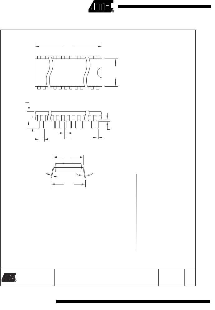
40P6
D
PIN 1
E1
A
SEATING PLANE 
A1
L 

B

 B1 e
B1 e
|
E |
|
C |
0º ~ 15º |
REF |
|
|
eB
Notes: 1. This package conforms to JEDEC reference MS-011, Variation AC.
2.Dimensions D and E1 do not include mold Flash or Protrusion. Mold Flash or Protrusion shall not exceed 0.25 mm (0.010").
COMMON DIMENSIONS
(Unit of Measure = mm)
SYMBOL |
MIN |
NOM |
|
MAX |
NOTE |
|
|
|
|
|
|
A |
– |
– |
|
4.826 |
|
|
|
|
|
|
|
A1 |
0.381 |
– |
|
– |
|
|
|
|
|
|
|
D |
52.070 |
– |
|
52.578 |
Note 2 |
|
|
|
|
|
|
E |
15.240 |
– |
|
15.875 |
|
|
|
|
|
|
|
E1 |
13.462 |
– |
|
13.970 |
Note 2 |
|
|
|
|
|
|
B |
0.356 |
– |
|
0.559 |
|
|
|
|
|
|
|
B1 |
1.041 |
– |
|
1.651 |
|
|
|
|
|
|
|
L |
3.048 |
– |
|
3.556 |
|
|
|
|
|
|
|
C |
0.203 |
– |
|
0.381 |
|
|
|
|
|
|
|
eB |
15.494 |
– |
|
17.526 |
|
|
|
|
|
|
|
e |
|
2.540 TYP |
|
|
|
|
|
|
|
|
|
TITLE
|
2325 Orchard Parkway |
40P6, 40-lead (0.600"/15.24 mm Wide) Plastic Dual |
|
San Jose, CA 95131 |
|
R |
Inline Package (PDIP) |
09/28/01
DRAWING NO. REV.
40P6 B
306 ATmega32(L)
2503F–AVR–12/03
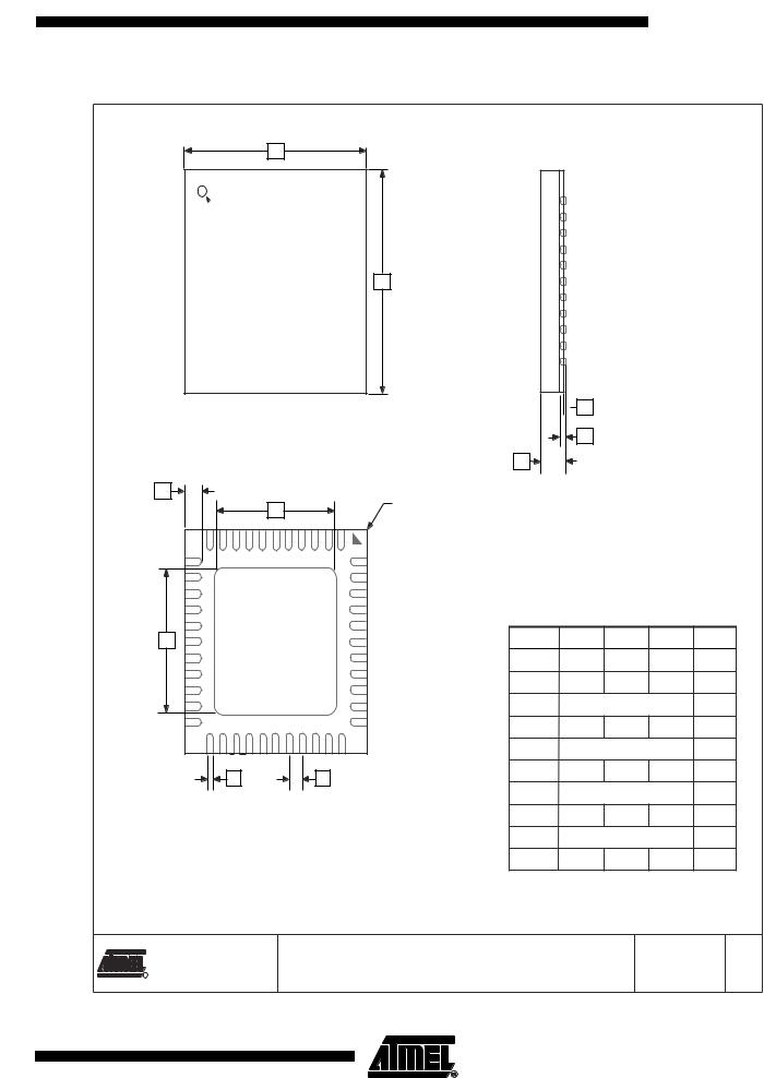
ATmega32(L)
44M1
D
 Marked Pin# 1 ID
E
 SEATING PLANE

 A1
A1
TOP VIEW
|
|
A3 |
|
|
|
A |
|
L |
Pin #1 Corner |
SIDE VIEW |
|
D2 |
|||
|
|
|
|
|
COMMON DIMENSIONS |
||
|
|
|
(Unit of Measure = mm) |
||
E2 |
|
SYMBOL |
MIN |
NOM |
MAX NOTE |
|
|
A |
0.80 |
0.90 |
1.00 |
|
|
A1 |
– |
0.02 |
0.05 |
|
|
A3 |
|
0.25 REF |
|
|
|
b |
0.18 |
0.23 |
0.30 |
|
|
D |
|
7.00 BSC |
|
b |
e |
D2 |
5.00 |
5.20 |
5.40 |
|
|
|
|
||
|
|
E |
|
7.00 BSC |
|
BOTTOM VIEW |
|
E2 |
5.00 |
5.20 |
5.40 |
|
|
||||
|
|
e |
|
0.50 BSC |
|
|
|
L |
0.35 |
0.55 |
0.75 |
Notes: 1. JEDEC Standard MO-220, Fig. 1 (SAW Singulation) VKKD-1.
TITLE
|
2325 Orchard Parkway |
44M1, 44-pad, 7 x 7 x 1.0 mm Body, Lead Pitch 0.50 mm |
|
San Jose, CA 95131 |
|
R |
Micro Lead Frame Package (MLF) |
01/15/03
DRAWING NO. REV.
44M1 C
307
2503F–AVR–12/03