

- •Features
- •Pin Configurations
- •Disclaimer
- •Overview
- •Block Diagram
- •Pin Descriptions
- •Port A (PA7..PA0)
- •Port B (PB7..PB0)
- •Port C (PC7..PC0)
- •Port D (PD7..PD0)
- •RESET
- •XTAL1
- •XTAL2
- •AVCC
- •AREF
- •AVR CPU Core
- •Introduction
- •Architectural Overview
- •Status Register
- •Stack Pointer
- •Interrupt Response Time
- •SRAM Data Memory
- •Data Memory Access Times
- •EEPROM Data Memory
- •EEPROM Read/Write Access
- •I/O Memory
- •Clock Systems and their Distribution
- •CPU Clock – clkCPU
- •I/O Clock – clkI/O
- •Flash Clock – clkFLASH
- •ADC Clock – clkADC
- •Clock Sources
- •Default Clock Source
- •Crystal Oscillator
- •External RC Oscillator
- •External Clock
- •Timer/Counter Oscillator
- •Idle Mode
- •Power-down Mode
- •Power-save Mode
- •Standby Mode
- •Extended Standby Mode
- •Analog to Digital Converter
- •Analog Comparator
- •Brown-out Detector
- •Internal Voltage Reference
- •Watchdog Timer
- •Port Pins
- •Resetting the AVR
- •Reset Sources
- •Power-on Reset
- •External Reset
- •Brown-out Detection
- •Watchdog Reset
- •Watchdog Timer
- •Interrupts
- •I/O Ports
- •Introduction
- •Configuring the Pin
- •Reading the Pin Value
- •Unconnected pins
- •Alternate Port Functions
- •Alternate Functions of Port A
- •Alternate Functions of Port B
- •Alternate Functions of Port C
- •Alternate Functions of Port D
- •Port A Data Register – PORTA
- •Port B Data Register – PORTB
- •Port C Data Register – PORTC
- •Port D Data Register – PORTD
- •External Interrupts
- •8-bit Timer/Counter0 with PWM
- •Overview
- •Registers
- •Definitions
- •Counter Unit
- •Output Compare Unit
- •Force Output Compare
- •Modes of Operation
- •Normal Mode
- •Fast PWM Mode
- •Phase Correct PWM Mode
- •Internal Clock Source
- •Prescaler Reset
- •External Clock Source
- •16-bit Timer/Counter1
- •Overview
- •Registers
- •Definitions
- •Compatibility
- •Counter Unit
- •Input Capture Unit
- •Input Capture Trigger Source
- •Noise Canceler
- •Using the Input Capture Unit
- •Output Compare Units
- •Force Output Compare
- •Modes of Operation
- •Normal Mode
- •Fast PWM Mode
- •Phase Correct PWM Mode
- •8-bit Timer/Counter2 with PWM and Asynchronous Operation
- •Overview
- •Registers
- •Definitions
- •Counter Unit
- •Output Compare Unit
- •Force Output Compare
- •Modes of Operation
- •Normal Mode
- •Fast PWM Mode
- •Phase Correct PWM Mode
- •Timer/Counter Prescaler
- •SS Pin Functionality
- •Slave Mode
- •Master Mode
- •SPI Control Register – SPCR
- •SPI Status Register – SPSR
- •SPI Data Register – SPDR
- •Data Modes
- •USART
- •Overview
- •AVR USART vs. AVR UART – Compatibility
- •Clock Generation
- •External Clock
- •Synchronous Clock Operation
- •Frame Formats
- •Parity Bit Calculation
- •USART Initialization
- •Parity Generator
- •Disabling the Transmitter
- •Receiver Error Flags
- •Parity Checker
- •Disabling the Receiver
- •Flushing the Receive Buffer
- •Asynchronous Data Recovery
- •Using MPCM
- •Write Access
- •Read Access
- •Two-wire Serial Interface
- •Features
- •TWI Terminology
- •Electrical Interconnection
- •Transferring Bits
- •START and STOP Conditions
- •Address Packet Format
- •Data Packet Format
- •Overview of the TWI Module
- •SCL and SDA Pins
- •Bit Rate Generator Unit
- •Bus Interface Unit
- •Address Match Unit
- •Control Unit
- •TWI Register Description
- •TWI Bit Rate Register – TWBR
- •TWI Control Register – TWCR
- •TWI Status Register – TWSR
- •TWI Data Register – TWDR
- •Using the TWI
- •Transmission Modes
- •Master Transmitter Mode
- •Master Receiver Mode
- •Slave Receiver Mode
- •Slave Transmitter Mode
- •Miscellaneous States
- •Analog Comparator
- •Analog Comparator Multiplexed Input
- •Features
- •Operation
- •Starting a Conversion
- •Differential Gain Channels
- •Changing Channel or Reference Selection
- •ADC Input Channels
- •ADC Voltage Reference
- •ADC Noise Canceler
- •Analog Input Circuitry
- •ADC Accuracy Definitions
- •ADC Conversion Result
- •ADLAR = 0
- •ADLAR = 1
- •Features
- •Overview
- •Test Access Port – TAP
- •TAP Controller
- •PRIVATE0; $8
- •PRIVATE1; $9
- •PRIVATE2; $A
- •PRIVATE3; $B
- •Bibliography
- •Features
- •System Overview
- •Data Registers
- •Bypass Register
- •Device Identification Register
- •Reset Register
- •Boundary-scan Chain
- •EXTEST; $0
- •IDCODE; $1
- •SAMPLE_PRELOAD; $2
- •AVR_RESET; $C
- •BYPASS; $F
- •Scanning the Digital Port Pins
- •Scanning the RESET Pin
- •Scanning the Clock Pins
- •Scanning the ADC
- •Features
- •Application Section
- •BLS – Boot Loader Section
- •Read-While-Write and no Read-While-Write Flash Sections
- •Boot Loader Lock Bits
- •Performing a Page Write
- •Using the SPM Interrupt
- •Setting the Boot Loader Lock Bits by SPM
- •Reading the Fuse and Lock Bits from Software
- •Preventing Flash Corruption
- •Fuse Bits
- •Latching of Fuses
- •Signature Bytes
- •Calibration Byte
- •Signal Names
- •Parallel Programming
- •Enter Programming Mode
- •Chip Erase
- •Programming the Flash
- •Programming the EEPROM
- •Reading the Flash
- •Reading the EEPROM
- •Programming the Lock Bits
- •Reading the Signature Bytes
- •Reading the Calibration Byte
- •SPI Serial Downloading
- •Data Polling Flash
- •Data Polling EEPROM
- •AVR_RESET ($C)
- •PROG_ENABLE ($4)
- •PROG_COMMANDS ($5)
- •PROG_PAGELOAD ($6)
- •PROG_PAGEREAD ($7)
- •Data Registers
- •Reset Register
- •Programming Enable Register
- •Virtual Flash Page Read Register
- •Programming Algorithm
- •Entering Programming Mode
- •Leaving Programming Mode
- •Performing Chip Erase
- •Programming the Flash
- •Reading the Flash
- •Programming the EEPROM
- •Reading the EEPROM
- •Programming the Fuses
- •Programming the Lock Bits
- •Reading the Signature Bytes
- •Reading the Calibration Byte
- •Electrical Characteristics
- •Absolute Maximum Ratings*
- •DC Characteristics
- •External Clock Drive Waveforms
- •External Clock Drive
- •Two-wire Serial Interface Characteristics
- •ADC Characteristics
- •Register Summary
- •Instruction Set Summary
- •Ordering Information
- •Packaging Information
- •Errata
- •ATmega32 Rev. A
- •Datasheet Change Log for ATmega32
- •Changes from Rev. 2503E-09/03 to Rev. 2503F-12/03
- •Changes from Rev. 2503D-02/03 to Rev. 2503E-09/03
- •Changes from Rev. 2503C-10/02 to Rev. 2503D-02/03
- •Changes from Rev. 2503B-10/02 to Rev. 2503C-10/02
- •Changes from Rev. 2503A-03/02 to Rev. 2503B-10/02
- •Table of Contents
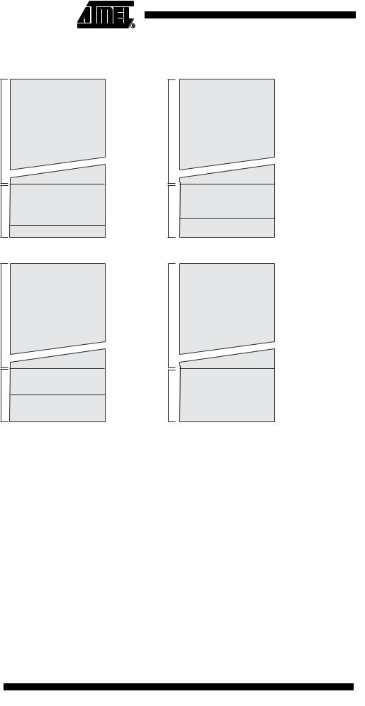
Figure 125. Memory Sections(1)
No Read-While-Write Section Read-While-Write Section No Read-While-Write Section Read-While-Write Section
Program Memory
BOOTSZ = '11'
Application Flash Section
Application Flash Section
Boot Loader Flash Section
Program Memory
BOOTSZ = '01'
Application Flash Section
Application Flash Section
Boot Loader Flash Section
$0000
End RWW
Start NRWW
End Application
Start Boot Loader
Flashend
$0000
End RWW
Start NRWW
End Application
Start Boot Loader
Flashend
No Read-While-Write Section Read-While-Write Section No Read-While-Write Section Read-While-Write Section
Program Memory
BOOTSZ = '10'
$0000
Application Flash Section
End RWW
Start NRWW
Application Flash Section
End Application
Start Boot Loader
Boot Loader Flash Section
Flashend
Program Memory BOOTSZ = '00'
$0000
Application flash Section
End RWW, End Application
Start NRWW, Start Boot Loader
Boot Loader Flash Section
Flashend
Note: 1. The parameters in the figure above are given in Table 100 on page 253.
Boot Loader Lock Bits If no Boot Loader capability is needed, the entire Flash is available for application code. The Boot Loader has two separate sets of Boot Lock bits which can be set independently. This gives the user a unique flexibility to select different levels of protection.
The user can select:
•To protect the entire Flash from a software update by the MCU
•To protect only the Boot Loader Flash section from a software update by the MCU
•To protect only the Application Flash section from a software update by the MCU
•Allow software update in the entire Flash
See Table 96 and Table 97 for further details. The Boot Lock bits can be set in software and in Serial or Parallel Programming mode, but they can be cleared by a Chip Erase command only. The general Write Lock (Lock Bit mode 2) does not control the programming of the Flash memory by SPM instruction. Similarly, the general Read/Write Lock (Lock Bit mode 3) does not control reading nor writing by LPM/SPM, if it is attempted.
244 ATmega32(L)
2503F–AVR–12/03

 ATmega32(L)
Entering the Boot Loader
Program
Table 96. Boot Lock Bit0 Protection Modes (Application Section)(1)
BLB0 Mode |
BLB02 |
BLB01 |
Protection |
|
|
|
|
|
|
1 |
1 |
1 |
No restrictions for SPM or LPM accessing the Application |
|
section. |
||||
|
|
|
||
|
|
|
|
|
2 |
1 |
0 |
SPM is not allowed to write to the Application section. |
|
|
|
|
|
|
|
|
|
SPM is not allowed to write to the Application section, and |
|
|
|
|
LPM executing from the Boot Loader section is not |
|
3 |
0 |
0 |
allowed to read from the Application section. If interrupt |
|
|
|
|
vectors are placed in the Boot Loader section, interrupts |
|
|
|
|
are disabled while executing from the Application section. |
|
|
|
|
|
|
|
|
|
LPM executing from the Boot Loader section is not |
|
4 |
0 |
1 |
allowed to read from the Application section. If interrupt |
|
vectors are placed in the Boot Loader section, interrupts |
||||
|
|
|
||
|
|
|
are disabled while executing from the Application section. |
|
|
|
|
|
|
Note: 1. “1” means unprogrammed, “0” means programmed |
||||
Table 97. Boot Lock Bit1 Protection Modes (Boot Loader Section)(1)
BLB1 mode |
BLB12 |
BLB11 |
Protection |
|
|
|
|
|
|
1 |
1 |
1 |
No restrictions for SPM or LPM accessing the Boot Loader |
|
section. |
||||
|
|
|
||
|
|
|
|
|
2 |
1 |
0 |
SPM is not allowed to write to the Boot Loader section. |
|
|
|
|
|
|
|
|
|
SPM is not allowed to write to the Boot Loader section, |
|
|
|
|
and LPM executing from the Application section is not |
|
3 |
0 |
0 |
allowed to read from the Boot Loader section. If interrupt |
|
|
|
|
vectors are placed in the Application section, interrupts |
|
|
|
|
are disabled while executing from the Boot Loader section. |
|
|
|
|
|
|
|
|
|
LPM executing from the Application section is not allowed |
|
4 |
0 |
1 |
to read from the Boot Loader section. If interrupt vectors |
|
are placed in the Application section, interrupts are |
||||
|
|
|
||
|
|
|
disabled while executing from the Boot Loader section. |
|
|
|
|
|
|
Note: 1. “1” means unprogrammed, “0” means programmed |
||||
Entering the Boot Loader takes place by a jump or call from the application program. This may be initiated by a trigger such as a command received via USART, or SPI interface. Alternatively, the Boot Reset Fuse can be programmed so that the Reset Vector is pointing to the Boot Flash start address after a reset. In this case, the Boot Loader is started after a reset. After the application code is loaded, the program can start executing the application code. Note that the fuses cannot be changed by the MCU itself. This means that once the Boot Reset Fuse is programmed, the Reset Vector will always point to the Boot Loader Reset and the fuse can only be changed through the serial or parallel programming interface.
245
2503F–AVR–12/03

Table 98. Boot Reset Fuse(1)
BOOTRST |
Reset Address |
|
|
1 |
Reset Vector = Application reset (address $0000) |
|
|
0 |
Reset Vector = Boot Loader reset (see Table 100 on page 253) |
|
|
Note: 1. “1” means unprogrammed, “0” means programmed
Store Program Memory |
The Store Program Memory Control Register contains the control bits needed to control |
|||||||||
Control Register – SPMCR |
the Boot Loader operations. |
|
|
|
|
|
|
|
||
|
Bit |
7 |
6 |
5 |
4 |
3 |
2 |
1 |
0 |
|
|
|
|
|
|
|
|
|
|
|
SPMCR |
|
|
SPMIE |
RWWSB |
– |
RWWSRE |
BLBSET |
PGWRT |
PGERS |
SPMEN |
|
|
|
|
|
|
|
|
|
|
|
|
|
Read/Write |
R/W |
R |
R |
R/W |
R/W |
R/W |
R/W |
R/W |
|
|
Initial value |
0 |
0 |
0 |
0 |
0 |
0 |
0 |
0 |
|
• Bit 7 – SPMIE: SPM Interrupt Enable
When the SPMIE bit is written to one, and the I-bit in the Status Register is set (one), the SPM ready interrupt will be enabled. The SPM ready Interrupt will be executed as long as the SPMEN bit in the SPMCR Register is cleared.
• Bit 6 – RWWSB: Read-While-Write Section Busy
When a self-programming (Page Erase or Page Write) operation to the RWW section is initiated, the RWWSB will be set (one) by hardware. When the RWWSB bit is set, the RWW section cannot be accessed. The RWWSB bit will be cleared if the RWWSRE bit is written to one after a Self-Programming operation is completed. Alternatively the RWWSB bit will automatically be cleared if a page load operation is initiated.
• Bit 5 – Res: Reserved Bit
This bit is a reserved bit in the ATmega32 and always read as zero.
• Bit 4 – RWWSRE: Read-While-Write Section Read Enable
When programming (Page Erase or Page Write) to the RWW section, the RWW section is blocked for reading (the RWWSB will be set by hardware). To re-enable the RWW section, the user software must wait until the programming is completed (SPMEN will be cleared). Then, if the RWWSRE bit is written to one at the same time as SPMEN, the next SPM instruction within four clock cycles re-enables the RWW section. The RWW section cannot be re-enabled while the Flash is busy with a page erase or a page write (SPMEN is set). If the RWWSRE bit is written while the Flash is being loaded, the Flash load operation will abort and the data loaded will be lost.
• Bit 3 – BLBSET: Boot Lock Bit Set
If this bit is written to one at the same time as SPMEN, the next SPM instruction within four clock cycles sets Boot Lock bits, according to the data in R0. The data in R1 and the address in the Z-pointer are ignored. The BLBSET bit will automatically be cleared upon completion of the Lock bit set, or if no SPM instruction is executed within four clock cycles.
An LPM instruction within three cycles after BLBSET and SPMEN are set in the SPMCR Register, will read either the Lock bits or the Fuse bits (depending on Z0 in the Z- pointer) into the destination register. See “Reading the Fuse and Lock Bits from Software” on page 250 for details.
246 ATmega32(L)
2503F–AVR–12/03

Addressing the Flash during SelfProgramming
2503F–AVR–12/03
ATmega32(L)
• Bit 2 – PGWRT: Page Write
If this bit is written to one at the same time as SPMEN, the next SPM instruction within four clock cycles executes Page Write, with the data stored in the temporary buffer. The page address is taken from the high part of the Z-pointer. The data in R1 and R0 are ignored. The PGWRT bit will auto-clear upon completion of a page write, or if no SPM instruction is executed within four clock cycles. The CPU is halted during the entire page write operation if the NRWW section is addressed.
• Bit 1 – PGERS: Page Erase
If this bit is written to one at the same time as SPMEN, the next SPM instruction within four clock cycles executes Page Erase. The page address is taken from the high part of the Z-pointer. The data in R1 and R0 are ignored. The PGERS bit will auto-clear upon completion of a page erase, or if no SPM instruction is executed within four clock cycles. The CPU is halted during the entire page write operation if the NRWW section is addressed.
• Bit 0 – SPMEN: Store Program Memory Enable
This bit enables the SPM instruction for the next four clock cycles. If written to one together with either RWWSRE, BLBSET, PGWRT’ or PGERS, the following SPM instruction will have a special meaning, see description above. If only SPMEN is written, the following SPM instruction will store the value in R1:R0 in the temporary page buffer addressed by the Z-pointer. The LSB of the Z-pointer is ignored. The SPMEN bit will auto-clear upon completion of an SPM instruction, or if no SPM instruction is executed within four clock cycles. During page erase and page write, the SPMEN bit remains high until the operation is completed.
Writing any other combination than “10001”, “01001”, “00101”, “00011” or “00001” in the lower five bits will have no effect.
The Z-pointer is used to address the SPM commands.
Bit |
15 |
14 |
13 |
12 |
11 |
10 |
9 |
8 |
ZH (R31) |
Z15 |
Z14 |
Z13 |
Z12 |
Z11 |
Z10 |
Z9 |
Z8 |
ZL (R30) |
|
|
|
|
|
|
|
|
Z7 |
Z6 |
Z5 |
Z4 |
Z3 |
Z2 |
Z1 |
Z0 |
|
|
|
|
|
|
|
|
|
|
|
7 |
6 |
5 |
4 |
3 |
2 |
1 |
0 |
Since the Flash is organized in pages (see Table 111 on page 258), the Program Counter can be treated as having two different sections. One section, consisting of the least significant bits, is addressing the words within a page, while the most significant bits are addressing the pages. This is shown in Figure 126. Note that the Page Erase and Page Write operations are addressed independently. Therefore it is of major importance that the Boot Loader software addresses the same page in both the Page Erase and Page Write operation. Once a programming operation is initiated, the address is latched and the Z-pointer can be used for other operations.
The only SPM operation that does not use the Z-pointer is Setting the Boot Loader Lock bits. The content of the Z-pointer is ignored and will have no effect on the operation. The LPM instruction does also use the Z pointer to store the address. Since this instruction addresses the Flash byte by byte, also the LSB (bit Z0) of the Z-pointer is used.
247

Figure 126. Addressing the Flash during SPM(1)
BIT 15 |
|
ZPCMSB |
ZPAGEMSB 1 0 |
|
|||||||||||||
Z - REGISTER |
|
|
|
|
|
|
|
|
|
|
|
0 |
|
|
|
|
|
|
|
|
|
|
|
|
|
|
|
|
|
|
|
|
|
|
|
|
PROGRAM |
|
PCMSB |
PAGEMSB |
|
|
|
|
|||||||||
|
|
PCPAGE |
PCWORD |
|
|
|
|
|
|||||||||
|
COUNTER |
|
|
|
|
|
|||||||||||
|
|
|
|
|
|
|
|
|
|
|
|
|
|
|
|||
|
|
PAGE ADDRESS |
|
|
WORD ADDRESS |
|
|||||||||||
|
|
WITHIN THE FLASH |
|
|
WITHIN A PAGE |
|
|||||||||||
PROGRAM MEMORY |
|
|
|
|
|
|
|
PAGE |
PCWORD[PAGEMSB:0]: |
||||||||
|
|
|
|
|
|
|
|
|
|
|
|
|
|
|
|
|
|
|
|
PAGE |
|
|
|
|
|
|
|
|
|
INSTRUCTION WORD |
00 |
||||
|
|
|
|
|
|
|
|
|
|
|
|
|
|||||
|
|
|
|
|
|
|
|
|
|
|
|
|
|
|
|
|
01 |
|
|
|
|
|
|
|
|
|
|
|
|
|
|
|
|
|
|
|
|
|
|
|
|
|
|
|
|
|
|
|
|
|
|
|
02 |
|
|
|
|
|
|
|
|
|
|
|
|
|
|
|
|
|
|
|
|
|
|
|
|
|
|
|
|
|
|
|
|
|
|
|
|
|
|
|
|
|
|
|
|
|
|
|
|
|
|
|
|
|
|
|
|
|
|
|
|
|
|
|
|
|
|
|
|
|
|
|
|
|
|
|
|
|
|
|
|
|
|
|
|
|
|
|
|
|
|
|
|
|
|
|
|
|
|
|
|
|
|
|
|
|
|
|
|
|
|
|
|
|
|
|
|
|
|
|
|
|
|
|
|
|
|
|
|
|
|
|
|
|
|
|
|
|
|
|
|
|
|
|
|
|
|
|
|
|
|
|
|
|
|
|
|
|
|
|
|
|
|
|
|
|
|
|
|
|
|
|
|
|
|
|
|
|
|
|
|
|
|
|
|
|
|
|
|
|
|
|
|
|
|
|
|
|
|
|
|
|
|
|
|
|
|
|
|
|
|
|
|
|
|
|
|
|
|
|
|
|
|
|
|
|
|
|
|
|
|
|
|
|
|
|
|
|
|
|
|
|
|
|
|
|
|
|
|
|
|
|
|
PAGEEND
Self-Programming the
Flash
Note: 1. The different variables used in Figure 126 are listed in Table 102 on page 253.
The program memory is updated in a page by page fashion. Before programming a page with the data stored in the temporary page buffer, the page must be erased. The temporary page buffer is filled one word at a time using SPM and the buffer can be filled either before the page erase command or between a page erase and a page write operation:
Alternative 1, fill the buffer before a Page Erase
•Fill temporary page buffer
•Perform a Page Erase
•Perform a Page Write
Alternative 2, fill the buffer after Page Erase
•Perform a Page Erase
•Fill temporary page buffer
•Perform a Page Write
If only a part of the page needs to be changed, the rest of the page must be stored (for example in the temporary page buffer) before the erase, and then be rewritten. When using alternative 1, the Boot Loader provides an effective Read-Modify-Write feature which allows the user software to first read the page, do the necessary changes, and then write back the modified data. If alternative 2 is used, it is not possible to read the old data while loading since the page is already erased. The temporary page buffer can be accessed in a random sequence. It is essential that the page address used in both the page erase and page write operation is addressing the same page. See “Simple Assembly Code Example for a Boot Loader” on page 251 for an assembly code example.
248 ATmega32(L)
2503F–AVR–12/03