


ATmega32(L)
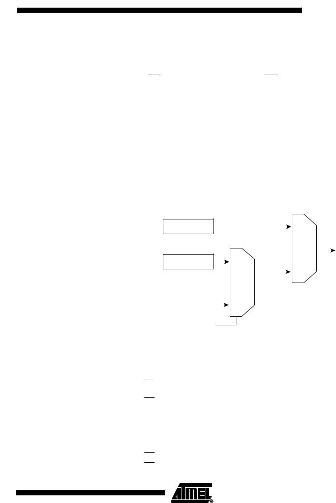
Programming the EEPROM The EEPROM is organized in pages, see Table 112 on page 258. When programming the EEPROM, the program data is latched into a page buffer. This allows one page of data to be programmed simultaneously. The programming algorithm for the EEPROM data memory is as follows (refer to “Programming the Flash” on page 260 for details on Command, Address and Data loading):
1.A: Load Command “0001 0001”.
2.G: Load Address High Byte ($00 - $FF)
3.B: Load Address Low Byte ($00 - $FF)
4.C: Load Data ($00 - $FF)
5.E: Latch data (give PAGEL a positive pulse)
K:Repeat 3 through 5 until the entire buffer is filled
L:Program EEPROM page
1.Set BS1 to “0”.
2.Give WR a negative pulse. This starts programming of the EEPROM page. RDY/BSY goes low.
3.Wait until to RDY/BSY goes high before programming the next page. (See Figure 130 for signal waveforms)
Figure 130. Programming the EEPROM Waveforms
|
|
|
|
|
|
|
|
|
|
|
|
|
|
K |
|
|
|
|
|
|
|
|
|
|
|
A |
G |
B |
C |
E |
B |
C |
E |
L |
|
|
|
|
DATA |
0x11 |
ADDR. HIGH ADDR. LOW |
DATA |
XX |
ADDR. LOW |
DATA |
XX |
|
|
|||||
|
|
|
|
|
|
|
|
|
|
|
|
|
|||||
|
|
|
|
XA1 |
|
|
|
|
|
|
|
|
|
|
|||
|
|
|
|
XA0 |
|
|
|
|
|
|
|
|
|
|
|||
|
|
|
|
BS1 |
|
|
|
|
|
|
|
|
|
|
|||
|
|
|
XTAL1 |
|
|
|
|
|
|
|
|
|
|
||||
|
|
|
|
|
|
|
|
|
|
|
|
|
|
|
|
|
|
|
|
|
|
|
WR |
|
|
|
|
|
|
|
|
|
|
|
|
|
|
|
|
|
|
|
|
|
|
|
|
|
|
|
|
|
|
|
|
RDY/BSY |
|
|
|
|
|
|
|
|
|
|
|
||||
|
|
|
|
|
|
|
|
|
|
|
|
|
|
|
|
|
|
|
|
|
|
|
|
|
|
|
|
|
|
|
|||||
|
|
RESET |
+12V |
|
|
|
|
|
|
|
|
|
|
||||
|
|
|
|
|
|
|
|
|
|
|
|
|
|
|
|
|
|
|
|
|
|
|
|
|
|
|
|
|
|
|
|
|
|
||
|
|
|
|
|
|
OE |
|
|
|
|
|
|
|
|
|
|
|
|
|
PAGEL |
|
|
|
|
|
|
|
|
|
|
|||||
|
|
|
|
BS2 |
|
|
|
|
|
|
|
|
|
|
|||
Reading the Flash |
The algorithm for reading the Flash memory is as follows (refer to “Programming the |
||||||||||||||||
|
Flash” on page 260 for details on Command and Address loading): |
|
|
||||||||||||||
1.A: Load Command “0000 0010”.
2.G: Load Address High Byte ($00 - $FF)
3.B: Load Address Low Byte ($00 - $FF)
4.Set OE to “0”, and BS1 to “0”. The Flash word low byte can now be read at DATA.
5.Set BS1 to “1”. The Flash word high byte can now be read at DATA.
263
2503F–AVR–12/03

|
|
|
|
|
|
|
|
|
|
|
|
|
|
|
|
|
|
|
|
|
|
|
|
|
|
|
|
|
|
|
|
|
|
|
|
|
|
|
|
6. |
Set OE to “1”. |
||||||||||
Reading the EEPROM |
The algorithm for reading the EEPROM memory is as follows (refer to “Programming the |
|||||||||||
|
Flash” on page 260 for details on Command and Address loading): |
|||||||||||
|
1. |
A: Load Command “0000 0011”. |
||||||||||
|
2. |
G: Load Address High Byte ($00 - $FF) |
||||||||||
|
3. |
B: Load Address Low Byte ($00 - $FF) |
||||||||||
|
4. |
Set |
|
|
to “0”, and BS1 to “0”. The EEPROM Data byte can now be read at |
|||||||
|
OE |
|||||||||||
|
|
DATA. |
||||||||||
|
5. |
Set |
|
|
to “1”. |
|||||||
|
OE |
|||||||||||
Programming the Fuse Low |
The algorithm for programming the Fuse Low bits is as follows (refer to “Programming |
|||||||||||
Bits |
the Flash” on page 260 for details on Command and Data loading): |
|||||||||||
|
1. |
A: Load Command “0100 0000”. |
||||||||||
|
2. |
C: Load Data Low Byte. Bit n = “0” programs and bit n = “1” erases the Fuse bit. |
||||||||||
|
3. |
Set BS1 to “0” and BS2 to “0”. |
||||||||||
|
4. |
Give |
|
|
|
to go high. |
||||||
|
WR |
a negative pulse and wait for RDY/BSY |
||||||||||
Programming the Fuse High |
The algorithm for programming the Fuse high bits is as follows (refer to “Programming |
|||||||||||
Bits |
the Flash” on page 260 for details on Command and Data loading): |
|||||||||||
|
1. |
A: Load Command “0100 0000”. |
||||||||||
|
2. |
C: Load Data Low Byte. Bit n = “0” programs and bit n = “1” erases the Fuse bit. |
||||||||||
|
3. |
Set BS1 to “1” and BS2 to “0”. This selects high data byte. |
||||||||||
|
4. |
Give |
|
|
|
to go high. |
||||||
|
WR |
a negative pulse and wait for RDY/BSY |
||||||||||
|
5. |
Set BS1 to “0”. This selects low data byte. |
||||||||||
Figure 131. Programming the Fuses
|
|
|
Write Fuse Low byte |
|
|
Write Fuse high byte |
|
A |
C |
|
A |
C |
|
DATA |
$40 |
DATA |
XX |
$40 |
DATA |
XX |
|
|
|
|
|
|
XA1
XA0
BS1
BS2
XTAL1
WR
RDY/BSY
RESET +12V
OE
PAGEL
264 ATmega32(L)
2503F–AVR–12/03
ATmega32(L)
Programming the Lock Bits The algorithm for programming the Lock bits is as follows (refer to “Programming the Flash” on page 260 for details on Command and Data loading):
1.A: Load Command “0010 0000”.
2.C: Load Data Low Byte. Bit n = “0” programs the Lock bit.
3.Give WR a negative pulse and wait for RDY/BSY to go high.
The Lock bits can only be cleared by executing Chip Erase.
Reading the Fuse and Lock |
The algorithm for reading the Fuse and Lock bits is as follows (refer to “Programming |
||||||||||||||||
Bits |
the Flash” on page 260 for details on Command loading): |
||||||||||||||||
|
1. |
A: Load Command “0000 0100”. |
|
|
|
|
|
|
|
|
|
||||||
|
2. |
Set |
|
to “0”, BS2 to “0” and BS1 to “0”. The status of the Fuse Low bits can |
|||||||||||||
|
OE |
||||||||||||||||
|
|
now be read at DATA (“0” means programmed). |
|||||||||||||||
|
3. |
Set |
|
to “0”, BS2 to “1” and BS1 to “1”. The status of the Fuse High bits can |
|||||||||||||
|
OE |
||||||||||||||||
|
|
now be read at DATA (“0” means programmed). |
|||||||||||||||
|
4. |
Set |
|
to “0”, BS2 to “0” and BS1 to “1”. The status of the Lock bits can now be |
|||||||||||||
|
OE |
||||||||||||||||
|
|
read at DATA (“0” means programmed). |
|||||||||||||||
|
5. |
Set |
|
to “1”. |
|
|
|
|
|
|
|
|
|
||||
|
OE |
|
|
|
|
|
|
|
|
|
|||||||
|
Figure 132. Mapping between BS1, BS2 and the Fuseand Lock Bits during Read |
||||||||||||||||
|
|
|
|
|
Fuse Low Byte |
|
|
0 |
DATA |
||||||||
|
|
|
|
|
|
|
|||||||||||
|
|
|
|
|
|
|
|
|
|
|
|
|
|
|
|
||
|
|
|
|
|
Lock Bits |
|
|
0 |
|
|
|
|
1 |
|
|
||
|
|
|
|
|
|
|
|
|
|
|
|
|
|
||||
|
|
|
|
|
|
|
|
|
|
|
|
||||||
|
|
|
|
|
|
|
|
|
|
|
|
|
|
||||
|
|
|
|
|
|
|
|
|
|
|
|
|
|||||
|
|
|
|
|
|
|
|
|
|
|
|
|
|
|
|
|
|
|
|
|
|
|
|
|
|
|
|
|
BS1 |
|
|
|
|||
|
|
|
|
|
Fuse High Byte |
|
|
|
1 |
||||||||
|
|
|
|
|
|
|
|
|
|
|
|
|
|
|
|
||
|
|
|
|
|
|
|
|
|
|
|
|
|
|
|
|
||
|
|
|
|
|
|
|
|
|
|
|
|
|
|
|
|
||
|
|
|
|
|
|
|
|
|
|
|
|
|
|
|
|
|
|
BS2
Reading the Signature Bytes The algorithm for reading the Signature bytes is as follows (refer to “Programming the Flash” on page 260 for details on Command and Address loading):
1.A: Load Command “0000 1000”.
2.B: Load Address Low Byte ($00 - $02).
3.Set OE to “0”, and BS1 to “0”. The selected Signature byte can now be read at DATA.
4.Set OE to “1”.
Reading the Calibration Byte The algorithm for reading the Calibration byte is as follows (refer to “Programming the Flash” on page 260 for details on Command and Address loading):
1.A: Load Command “0000 1000”.
2.B: Load Address Low Byte, $00.
3.Set OE to “0”, and BS1 to “1”. The Calibration byte can now be read at DATA.
4.Set OE to “1”.
265
2503F–AVR–12/03
|
|
|
|
|
|
|
|
|
|
|
|
|
|
|
|
|
|
|
|
|
|
|
|
|
|
|
|
|
|
|
|
|
|
|
|
|
|
|
|
|
|
|
|
|
|
|
|
|
|
|
|
|
|
|
|
|
|
|
|
|
|
|
|
|
|
|
|
|
|
|
|
|
|
|
|
|
|
|
|
|
|
|
|
|
|
|
|
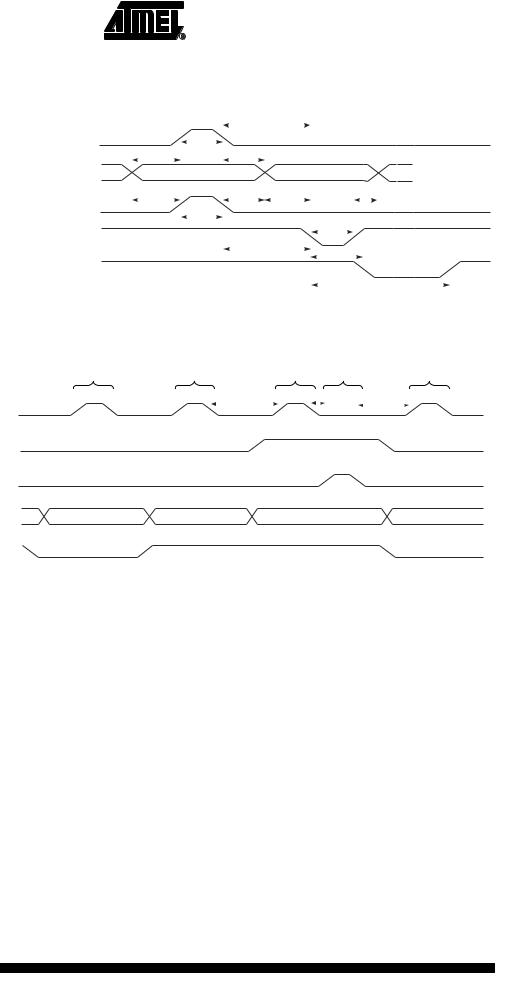
Parallel Programming |
Figure 133. Parallel Programming Timing, Including some General Timing |
||||||||||||||||||||||||||||||||||||||||||
Characteristics |
Requirements |
|
|
|
|
|
|
|
|
|
|
|
|
|
|
|
|
|
|
|
|
|
|
|
|
|
|
|
|
|
|
|
|
|
|
||||||||
|
|
|
|
|
|
|
|
|
|
|
|
|
|
|
|
|
|
|
tXLWL |
|
|
|
|
|
|
|
|
|
|
|
|
|
|
|
|
|
|
|
|
|
|
|
|
|
|
XTAL1 |
|
|
|
tXHXL |
|
|
|
|
|
|
|
|
|
|
|
|
|
|
|
|
|
|
|
|
|
|
|
|
|
|
|||||||||||
|
|
|
|
|
|
|
|
|
|
|
|
|
|
|
|
|
|
|
|
|
|
|
|
|
|
|
|
|
|
|
|
|
|
|
|
||||||||
|
|
Data & Contol |
|
tDVXH |
|
|
|
|
|
|
|
|
|
tXLDX |
|
|
|
|
|
|
|
|
|
|
|
|
|
|
|
|
|
|
|
|
|
|
|
||||||
|
|
|
|
|
|
|
|
|
|
|
|
|
|
|
|
|
|
|
|
|
|
|
|
|
|
|
|
|
|
|
|
|
|
|
|
|
|
|
|
||||
|
|
|
|
|
|
|
|
|
|
|
|
|
|
|
|
|
|
|
|
|
|
|
|
|
|
|
|
|
|
|
|
|
|
|
|
|
|
|
|
||||
|
(DATA, XA0/1, BS1, BS2) |
|
|
|
|
|
|
|
|
|
|
|
|
|
|
|
|
|
|
|
|
|
|
|
|
|
|
|
|
|
|
|
|
|
|
|
|
||||||
|
|
|
|
|
|
|
tBVPH |
|
|
|
|
|
|
|
|
|
tPLBX |
|
t BVWL |
|
|
|
|
|
|
|
|
|
|
tWLBX |
|
|
|
||||||||||
|
|
|
|
|
|
|
|
|
|
|
|
|
|
|
|
|
|
|
|
|
|
|
|
|
|
|
|
|
|
|
|
|
|
|
|
|
|
|
|
||||
|
|
PAGEL |
|
|
|
tPHPL |
|
|
|
|
|
|
|
|
tWL WH |
|
|
|
|
|
|
|
|
|
|
|
|
|
|||||||||||||||
|
|
|
|
|
|
|
|
|
|
|
|
|
|
|
|
|
|
|
|
|
|
|
|
|
|
|
|
|
|
|
|
|
|
|
|
|
|
|
|||||
|
|
|
WR |
|
|
|
|
|
|
|
|
|
tPLWL |
|
|
|
|
|
|
|
|
|
|
|
|
|
|
|
|
|
|
|
|
|
|
|
|||||||
|
|
|
|
|
|
|
|
|
|
|
|
|
|
|
|
|
|
|
|
|
|
|
|
WLRL |
|
|
|
|
|
|
|
|
|
||||||||||
|
|
|
|
|
|
|
|
|
|
|
|
|
|
|
|
|
|
|
|
|
|
|
|
|
|
|
|
|
|
|
|
|
|
|
|
||||||||
|
|
|
|
|
|
|
|
|
|
|
|
|
|
|
|
|
|
|
|
|
|
|
|
|
|
|
|
|
|
|
|
|
|
|
|
|
|
|
|
|
|
|
|
|
|
RDY/BSY |
|
|
|
|
|
|
|
|
|
|
|
|
|
|
|
|
|
|
|
|
|
|
|
|
|
|
|
|
|
|
|
|
|
|
|||||||
|
|
|
|
|
|
|
|
|
|
|
|
|
|
|
|
|
|
|
|
|
|
|
|
|
|
|
|
|
|
|
|
|
|
|
|
|
|
|
|
|
tWLRH |
||
|
|
|
|
|
|
|
|
|
|
|
|
|
|
|
|
|
|
|
|
|
|
|
|
|
|
|
|
|
|
|
|
|
|
|
|
|
|
|
|
|
|||
|
Figure 134 . Parallel Programming Timing, Loading Sequence with Timing |
||||||||||||||||||||||||||||||||||||||||||
|
Requirements(1) |
|
|
|
|
|
|
|
|
|
|
|
|
|
|
|
|
|
|
|
|
|
|
|
|
|
|
|
|
|
|
|
|
|
|
||||||||
|
|
LOAD ADDRESS |
LOAD DATA |
|
|
LOAD DATA LOAD DATA |
|
|
LOAD ADDRESS |
||||||||||||||||||||||||||||||||||
|
|
(LOW BYTE) |
(LOW BYTE) |
|
(HIGH BYTE) |
|
|
|
(LOW BYTE) |
||||||||||||||||||||||||||||||||||
|
|
|
|
|
|
|
|
|
|
|
|
|
|
|
|
|
|
|
t XLXH |
|
|
|
|
|
|
tXLPH |
tPLXH |
|
|
|
|
|
|||||||||||
|
XTAL1 |
|
|
|
|
|
|
|
|
|
|
|
|
|
|
|
|
|
|
|
|
|
|
|
|
|
|
|
|
|
|
|
|
|
|
|
|
|
|
|
|
|
|
|
BS1 |
|
|
|
|
|
|
|
|
|
|
|
|
|
|
|
|
|
|
|
|
|
|
|
|
|
|
|
|
|
|
|
|
|
|
|
|
|
|
|
|
|
|
|
PAGEL |
|
|
|
|
|
|
|
|
|
|
|
|
|
|
|
|
|
|
|
|
|
|
|
|
|
|
|
|
|
|
|
|
|
|
|
|
|
|
|
|
|
|
|
DATA |
ADDR0 (Low Byte) |
|
DATA (Low Byte) |
|
|
|
DATA (High Byte) |
|
|
|
|
ADDR1 (Low Byte) |
||||||||||||||||||||||||||||||
|
XA0 |
|
|
|
|
|
|
|
|
|
|
|
|
|
|
|
|
|
|
|
|
|
|
|
|
|
|
|
|
|
|
|
|
|
|
|
|
|
|
|
|
|
|
|
XA1 |
|
|
|
|
|
|
|
|
|
|
|
|
|
|
|
|
|
|
|
|
|
|
|
|
|
|
|
|
|
|
|
|
|
|
|
|
|
|
|
|
|
|
|
Note: |
1. The timing requirements shown in Figure 133 (i.e., tDVXH, tXHXL, and tXLDX) also apply |
|||||||||||||||||||||||||||||||||||||||||
|
|
to loading operation. |
|
|
|
|
|
|
|
|
|
|
|
|
|
|
|
|
|
|
|
|
|
|
|
|
|
|
|
|
|
|
|
|
|
|
|||||||
266 ATmega32(L)
2503F–AVR–12/03

 ATmega32(L)
Figure 135. Parallel Programming Timing, Reading Sequence (within the Same Page) with Timing Requirements(1)
|
|
|
|
|
LOAD ADDRESS |
READ DATA |
READ DATA |
LOAD ADDRESS |
||||||||||||||||||||||||||||||
|
|
|
|
|
(LOW BYTE) |
(LOW BYTE) |
(HIGH BYTE) |
|
(LOW BYTE) |
|
||||||||||||||||||||||||||||
|
|
|
|
|
|
|
tXLOL |
|
|
|
|
|
|
|
|
|
|
|
|
|
|
|
||||||||||||||||
XTAL1 |
|
|
|
|
|
|
|
|
|
|
|
|
|
|
|
|
|
|
|
|
|
|
|
|
|
|
|
|
|
|
|
|
|
|
|
|
||
BS1 |
|
|
|
|
|
|
|
|
|
|
|
|
|
|
|
|
|
|
|
|
|
|
tBVDV |
|
|
|
|
|
|
|
|
|
|
|
||||
|
|
|
|
|
|
|
|
|
|
|
|
|
|
|
|
|
|
|
|
|
|
|
|
|
|
|
|
|
|
|
|
|
|
|
|
|||
|
|
|
|
|
|
|
|
|
|
tOLDV |
|
|
|
|
|
|
|
|
|
|
|
|
|
|
|
|||||||||||||
|
|
|
|
|
|
|
|
|
|
|
|
|
|
|
|
|
|
|
|
|
|
|
|
|
||||||||||||||
|
|
|
|
|
|
|
|
|
|
|
|
|
|
|
|
|
|
|
|
|
|
|
|
|
|
|
|
|
|
|
|
|
|
|
|
|
||
|
OE |
|
|
|
|
|
|
|
|
|
|
|
|
|
|
|
|
|
|
|
|
|
|
|
|
|
|
|
|
|
tOHDZ |
|
|
|
|
|
||
|
|
|
|
|
|
|
|
|
|
|
|
|
|
|
|
|
|
|
|
|
|
|
|
|
|
|
|
|
|
|
|
|
ADDR1 (Low Byte) |
|||||
|
|
|
|
|
|
|
|
|
|
|
|
|
|
|
|
|||||||||||||||||||||||
DATA |
|
|
ADDR0 (Low Byte) |
|
|
|
DATA (Low Byte) |
|
DATA (High Byte) |
|
|
|||||||||||||||||||||||||||
XA0 |
|
|
|
|
|
|
|
|
|
|
|
|
|
|
|
|
|
|
|
|
|
|
|
|
|
|
|
|
|
|
|
|
|
|
|
|
||
|
|
|
|
|
|
|
|
|
|
|
|
|
|
|
|
|
|
|
|
|
|
|
|
|
|
|
|
|
|
|
|
|
|
|
|
|||
XA1 |
|
|
|
|
|
|
|
|
|
|
|
|
|
|
|
|
|
|
|
|
|
|
|
|
|
|
|
|
|
|
|
|
|
|
|
|
||
Note: 1. |
The timing requirements shown in Figure 133 (i.e., tDVXH, tXHXL, and tXLDX) also apply |
|||||||||||||||||||||||||||||||||||||
|
|
|
to reading operation. |
|
|
|
|
|
|
|
|
|
|
|
|
|
|
|
||||||||||||||||||||
Table 113. |
|
Parallel Programming Characteristics, VCC = 5 V ± 10% |
|
|
|
|
||||||||||||||||||||||||||||||||
Symbol |
|
Parameter |
|
|
|
|
|
|
Min |
Typ |
|
Max |
|
Units |
||||||||||||||||||||||||
|
|
|
|
|
|
|
|
|
|
|
|
|
|
|
|
|
|
|
|
|
|
|
|
|
|
|
||||||||||||
VPP |
|
|
Programming Enable Voltage |
|
11.5 |
|
|
|
|
|
12.5 |
|
V |
|||||||||||||||||||||||||
IPP |
|
|
Programming Enable Current |
|
|
|
|
|
|
|
250 |
|
A |
|||||||||||||||||||||||||
tDVXH |
|
|
Data and Control Valid before XTAL1 High |
|
67 |
|
|
|
|
|
|
|
ns |
|||||||||||||||||||||||||
tXLXH |
|
|
XTAL1 Low to XTAL1 High |
|
|
|
|
|
|
200 |
|
|
|
|
|
|
|
ns |
||||||||||||||||||||
tXHXL |
|
|
XTAL1 Pulse Width High |
|
|
|
|
|
|
150 |
|
|
|
|
|
|
|
ns |
||||||||||||||||||||
tXLDX |
|
|
Data and Control Hold after XTAL1 Low |
|
67 |
|
|
|
|
|
|
|
ns |
|||||||||||||||||||||||||
tXLWL |
|
|
XTAL1 Low to |
|
|
|
|
|
|
Low |
|
|
|
|
|
|
0 |
|
|
|
|
|
|
|
ns |
|||||||||||||
WR |
|
|
|
|
|
|
|
|
||||||||||||||||||||||||||||||
tXLPH |
|
|
XTAL1 Low to PAGEL high |
|
|
|
|
|
|
0 |
|
|
|
|
|
|
|
ns |
||||||||||||||||||||
tPLXH |
|
|
PAGEL low to XTAL1 high |
|
|
|
|
|
|
150 |
|
|
|
|
|
|
|
ns |
||||||||||||||||||||
tBVPH |
|
|
BS1 Valid before PAGEL High |
|
67 |
|
|
|
|
|
|
|
ns |
|||||||||||||||||||||||||
tPHPL |
|
|
PAGEL Pulse Width High |
|
|
|
|
|
|
150 |
|
|
|
|
|
|
|
ns |
||||||||||||||||||||
tPLBX |
|
|
BS1 Hold after PAGEL Low |
|
67 |
|
|
|
|
|
|
|
ns |
|||||||||||||||||||||||||
tWLBX |
|
|
BS2/1 Hold after |
|
|
|
|
|
|
Low |
|
|
|
|
|
|
67 |
|
|
|
|
|
|
|
ns |
|||||||||||||
WR |
|
|
|
|
|
|
|
|
||||||||||||||||||||||||||||||
tPLWL |
|
|
PAGEL Low to |
|
|
|
|
|
|
|
Low |
|
|
|
|
|
|
67 |
|
|
|
|
|
|
|
ns |
||||||||||||
WR |
|
|
|
|
|
|
|
|
||||||||||||||||||||||||||||||
tBVWL |
|
|
BS1 Valid to |
|
|
|
|
|
|
Low |
|
|
|
|
|
|
67 |
|
|
|
|
|
|
|
ns |
|||||||||||||
WR |
|
|
|
|
|
|
|
|
||||||||||||||||||||||||||||||
tWLWH |
|
|
|
Pulse Width Low |
|
|
|
|
|
|
150 |
|
|
|
|
|
|
|
ns |
|||||||||||||||||||
|
|
WR |
|
|
|
|
|
|
|
|
||||||||||||||||||||||||||||
tWLRL |
|
|
|
|
|
|
|
|
|
|
|
|
|
|
|
|
|
|
|
|
Low |
|
|
|
|
|
|
0 |
|
|
|
|
|
1 |
|
s |
||
|
|
WR |
Low to RDY/BSY |
|
|
|
|
|
||||||||||||||||||||||||||||||
tWLRH |
|
|
|
|
|
|
|
|
|
|
|
|
|
|
|
|
|
|
|
|
High(1) |
|
3.7 |
|
|
|
|
|
4.5 |
|
ms |
|||||||
|
|
WR |
Low to RDY/BSY |
|||||||||||||||||||||||||||||||||||
tWLRH_CE |
|
|
|
|
|
|
|
|
|
|
|
|
|
|
|
|
|
|
|
|
High for Chip Erase(2) |
|
7.5 |
|
|
|
|
|
9 |
|
ms |
|||||||
|
|
WR |
Low to RDY/BSY |
|||||||||||||||||||||||||||||||||||
tXLOL |
|
|
XTAL1 Low to |
|
|
|
|
|
|
|
Low |
|
|
|
|
|
|
0 |
|
|
|
|
|
|
|
ns |
||||||||||||
|
|
OE |
|
|
|
|
|
|
|
|
||||||||||||||||||||||||||||
267
2503F–AVR–12/03