


Figure 56. Compare Match Output Unit, Schematic
COMn1
COMn0 Waveform
FOCn Generator
DATA BUS
clkI/O
|
|
|
|
|
|
|
|
|
|
|
|
|
|
|
|
|
|
|
|
D Q |
|
|
|
|
|
|
|
|
|
|
|
|
|
|
|
|
|
|
|
|
|
|
|
|
|
|
|
1 |
|
|
|
|
|
|
|
|
|
|
|
|
|
OCn |
|
|
OCn |
0 |
|
|
|
Pin |
|
|
|
|
|
|
|
|
||
 D Q
D Q
PORT
 D Q
D Q
DDR
|
The general I/O port function is overridden by the Output Compare (OC2) from the |
|
waveform generator if either of the COM21:0 bits are set. However, the OC2 pin direc- |
|
tion (input or output) is still controlled by the Data Direction Register (DDR) for the port |
|
pin. The Data Direction Register bit for the OC2 pin (DDR_OC2) must be set as output |
|
before the OC2 value is visible on the pin. The port override function is independent of |
|
the Waveform Generation mode. |
|
The design of the output compare pin logic allows initialization of the OC2 state before |
|
the output is enabled. Note that some COM21:0 bit settings are reserved for certain |
|
modes of operation. See “8-bit Timer/Counter Register Description” on page 123. |
Compare Output Mode and |
The waveform generator uses the COM21:0 bits differently in Normal, CTC, and PWM |
Waveform Generation |
modes. For all modes, setting the COM21:0 = 0 tells the Waveform Generator that no |
|
action on the OC2 Register is to be performed on the next compare match. For compare |
|
output actions in the non-PWM modes refer to Table 51 on page 124. For fast PWM |
|
mode, refer to Table 52 on page 124, and for phase correct PWM refer to Table 53 on |
|
page 124. |
|
A change of the COM21:0 bits state will have effect at the first compare match after the |
|
bits are written. For non-PWM modes, the action can be forced to have immediate effect |
|
by using the FOC2 strobe bits. |
Modes of Operation |
The mode of operation, i.e., the behavior of the Timer/Counter and the output compare |
|
pins, is defined by the combination of the Waveform Generation mode (WGM21:0) and |
|
Compare Output mode (COM21:0) bits. The Compare Output mode bits do not affect |
|
the counting sequence, while the Waveform Generation mode bits do. The COM21:0 |
|
bits control whether the PWM output generated should be inverted or not (inverted or |
|
non-inverted PWM). For non-PWM modes the COM21:0 bits control whether the output |
|
should be set, cleared, or toggled at a compare match (See “Compare Match Output |
|
Unit” on page 115.). |
|
For detailed timing information refer to “Timer/Counter Timing Diagrams” on page 121. |
116 ATmega32(L)
2503F–AVR–12/03
|
|
|
|
|
|
|
|
|
|
|
|
|
|
ATmega32(L) |
|||
|
|
|
|
|
|
|
|
|
|
|
|
|
|||||
|
Normal Mode |
|
|
|
|
|
|
|
|
|
|
|
|||||
|
The simplest mode of operation is the Normal mode (WGM21:0 = 0). In this mode the |
||||||||||||||||
|
|||||||||||||||||
|
|
counting direction is always up (incrementing), and no counter clear is performed. The |
|||||||||||||||
|
|
counter simply overruns when it passes its maximum 8-bit value (TOP = 0xFF) and then |
|||||||||||||||
|
|
restarts from the bottom (0x00). In normal operation the Timer/Counter Overflow Flag |
|||||||||||||||
|
|
(TOV2) will be set in the same timer clock cycle as the TCNT2 becomes zero. The TOV2 |
|||||||||||||||
|
|
Flag in this case behaves like a ninth bit, except that it is only set, not cleared. However, |
|||||||||||||||
|
|
combined with the timer overflow interrupt that automatically clears the TOV2 Flag, the |
|||||||||||||||
|
|
timer resolution can be increased by software. There are no special cases to consider in |
|||||||||||||||
|
|
the normal mode, a new counter value can be written anytime. |
|||||||||||||||
|
|
The Output Compare unit can be used to generate interrupts at some given time. Using |
|||||||||||||||
|
|
the output compare to generate waveforms in normal mode is not recommended, since |
|||||||||||||||
|
|
this will occupy too much of the CPU time. |
|||||||||||||||
|
Clear Timer on Compare |
In Clear Timer on Compare or CTC mode (WGM21:0 = 2), the OCR2 Register is used to |
|||||||||||||||
|
Match (CTC) Mode |
manipulate the counter resolution. In CTC mode the counter is cleared to zero when the |
|||||||||||||||
|
|
counter value (TCNT2) matches the OCR2. The OCR2 defines the top value for the |
|||||||||||||||
|
|
counter, hence also its resolution. This mode allows greater control of the compare |
|||||||||||||||
|
|
match output frequency. It also simplifies the operation of counting external events. |
|||||||||||||||
|
|
The timing diagram for the CTC mode is shown in Figure 57. The counter value |
|||||||||||||||
|
|
(TCNT2) increases until a compare match occurs between TCNT2 and OCR2, and then |
|||||||||||||||
|
|
counter (TCNT2) is cleared. |
|||||||||||||||
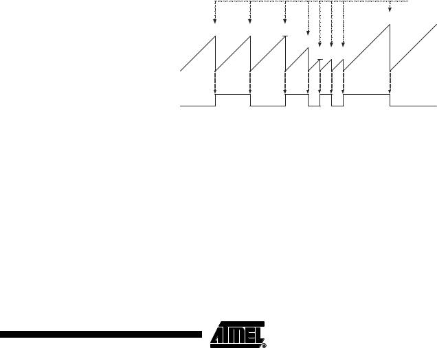
|
|
Figure 57. CTC Mode, Timing Diagram |
|||||||||||||||
|
|
|
|
|
|
|
|
|
|
|
|
|
|
|
|
|
|
|
|
|
|
|
|
|
|
|
|
|
|
|
|
|
|
OCn Interrupt Flag Set |
|
|
|
|
|
|
|
|
|
|
|
|
|
|
|
|
|
|
|
|
|
|
|
|
|
|
|
|
|
|
|
|
|
|
|
|
|
|
|
|
|
|
|
|
|
|
|
|
|
|
|
|
|
|
|
|
|
|
|
|
|
|
|
|
|
|
|
|
|
|
|
|
|
|
|
|
|
|
|
|
|
|
|
|
|
|
|
|
|
|
|
TCNTn
OCn
(COMn1:0 = 1)
(Toggle)
Period  1
1 
 2
2 
 3
3 
 4
4 

An interrupt can be generated each time the counter value reaches the TOP value by using the OCF2 Flag. If the interrupt is enabled, the interrupt handler routine can be used for updating the TOP value. However, changing the TOP to a value close to BOTTOM when the counter is running with none or a low prescaler value must be done with care since the CTC mode does not have the double buffering feature. If the new value written to OCR2 is lower than the current value of TCNT2, the counter will miss the compare match. The counter will then have to count to its maximum value (0xFF) and wrap around starting at 0x00 before the compare match can occur.
For generating a waveform output in CTC mode, the OC2 output can be set to toggle its logical level on each compare match by setting the Compare Output mode bits to toggle mode (COM21:0 = 1). The OC2 value will not be visible on the port pin unless the data direction for the pin is set to output. The waveform generated will have a maximum fre-
117
2503F–AVR–12/03
quency of fOC2 = fclk_I/O/2 when OCR2 is set to zero (0x00). The waveform frequency is defined by the following equation:
|
|
|
|
|
fOCn = |
|
fclk_I/O |
||||||||||
|
|
|
|
|
2--------N-- (1 + OCRn)------------------------------------ |
||||||||||||
|
The N variable represents the prescale factor (1, 8, 32, 64, 128, 256, or 1024). |
||||||||||||||||
|
As for the Normal mode of operation, the TOV2 Flag is set in the same timer clock cycle |
||||||||||||||||
|
that the counter counts from MAX to 0x00. |
||||||||||||||||
Fast PWM Mode |
The fast Pulse Width Modulation or fast PWM mode (WGM21:0 = 3) provides a high fre- |
||||||||||||||||
|
quency PWM waveform generation option. The fast PWM differs from the other PWM |
||||||||||||||||
|
option by its single-slope operation. The counter counts from BOTTOM to MAX then |
||||||||||||||||
|
restarts from BOTTOM. In non-inverting Compare Output mode, the Output Compare |
||||||||||||||||
|
(OC2) is cleared on the compare match between TCNT2 and OCR2, and set at BOT- |
||||||||||||||||
|
TOM. In inverting Compare Output mode, the output is set on compare match and |
||||||||||||||||
|
cleared at BOTTOM. Due to the single-slope operation, the operating frequency of the |
||||||||||||||||
|
fast PWM mode can be twice as high as the phase correct PWM mode that uses dual- |
||||||||||||||||
|
slope operation. This high frequency makes the fast PWM mode well suited for power |
||||||||||||||||
|
regulation, rectification, and DAC applications. High frequency allows physically small |
||||||||||||||||
|
sized external components (coils, capacitors), and therefore reduces total system cost. |
||||||||||||||||
|
In fast PWM mode, the counter is incremented until the counter value matches the MAX |
||||||||||||||||
|
value. The counter is then cleared at the following timer clock cycle. The timing diagram |
||||||||||||||||
|
for the fast PWM mode is shown in Figure 58. The TCNT2 value is in the timing diagram |
||||||||||||||||
|
shown as a histogram for illustrating the single-slope operation. The diagram includes |
||||||||||||||||
|
non-inverted and inverted PWM outputs. The small horizontal line marks on the TCNT2 |
||||||||||||||||
|
slopes represent compare matches between OCR2 and TCNT2. |
||||||||||||||||
|
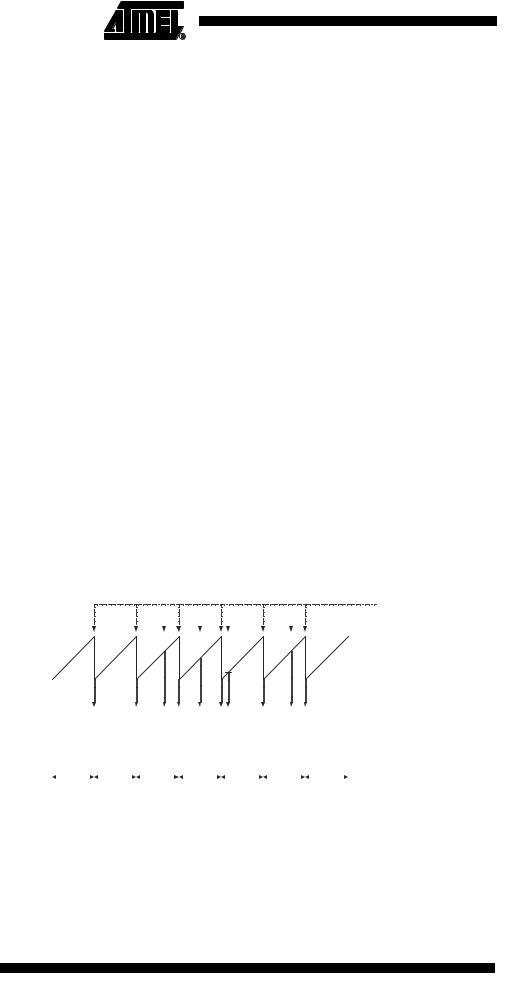
Figure 58. Fast PWM Mode, Timing Diagram |
||||||||||||||||
|
|
|
|
|
|
|
|
|
|
|
|
|
|
|
|
|
|
|
|
|
|
|
|
|
|
|
|
|
|
|
|
|
|
OCRn Interrupt Flag Set |
|
|
|
|
|
|
|
|
|
|
|
|
|
|
|
|
|
||
|
|
|
|
|
|
|
|
|
|
|
|
|
|
|
|
|
|
|
|
|
|
|
|
|
|
|
|
|
|
|
|
|
|
|
|
|
|
|
|
|
|
|
|
|
|
|
|
|
|
|
|
OCRn Update and |
|
|
|
|
|
|
|
|
|
|
|
|
|
|
|
|
|
TOVn Interrupt Flag Set |
|
|
|
|
|
|
|
|
|
|
|
|
|
|
|
|
|
|
|
|
|
|
|
|
|
|
|
|
|
|
|
|
|
|
|
|
|
|
|
|
|
|
|
|
|
|
|
|
|
|
|
|
|
|
|
|
|
|
|
|
|
|
|
|
|
|
|
|
|
|
|
|
|
TCNTn
OCn |
|
|
|
|
|
|
|
|
|
|
|
|
|
|
|
|
|
|
|
|
|
|
|
|
|
|
|
|
|
|
|
|
|
|
|
|
|
|
|
|
(COMn1:0 = 2) |
|
|
|
|
|
|
|
|
|
|
|
|
|
|
|
|
|
|
|
|
|
|
|
|
|
|
|
|
|
|
|
|
|
|
|
|
|
|
|
|
|
|
|
|
OCn |
|
|
|
|
|
|
|
|
|
|
|
|
|
|
|
|
|
|
|
|
|
|
|
|
|
|
|
|
|
|
|
|
|
|
|
|
|
|
|
|
(COMn1:0 = 3) |
|
Period |
|
|
|
|
|
|
|
|
|
|
|
|
|
|
|
|
|
|
|
|
|
|
|
|
|
|
|
|
|
|
|
|
|
|
|
|
|
|
|
|
|
|
|
|
|
|
|
|
|
|
|
|
|
|
|
|
|
|
|
|
|
|
|
|
|
|
|
|
|
|
|
|
|
|
|
|
|
|
|
|
|
|
|
||
|
|
1 |
|
|
|
|
2 |
|
|
|
|
3 |
|
|
|
|
|
4 |
|
|
|
|
|
5 |
|
|
|
|
6 |
|
|
|
|
|
7 |
|
|
|
|
|||
|
|
|
|
|
|
|
|
|
|
|
|
|
|
|
|
|
||||||||||||||||||||||||||
|
|
|
|
|
|
|
|
|
|
|
|
|
|
|
|
|
|
|
|
|
|
|
|
|
|
|
|
|
|
|
|
|
|
|
|
|
|
|
|
|
|
|
The Timer/Counter Overflow Flag (TOV2) is set each time the counter reaches MAX. If the interrupt is enabled, the interrupt handler routine can be used for updating the compare value.
In fast PWM mode, the compare unit allows generation of PWM waveforms on the OC2 pin. Setting the COM21:0 bits to 2 will produce a non-inverted PWM and an inverted PWM output can be generated by setting the COM21:0 to 3 (see Table 52 on page 124). The actual OC2 value will only be visible on the port pin if the data direction for the port
118 ATmega32(L)
2503F–AVR–12/03

 ATmega32(L)
pin is set as output. The PWM waveform is generated by setting (or clearing) the OC2 Register at the compare match between OCR2 and TCNT2, and clearing (or setting) the OC2 Register at the timer clock cycle the counter is cleared (changes from MAX to BOTTOM).
The PWM frequency for the output can be calculated by the following equation:
fclk_I/O fOC nP WM = -----------------
N 256
The N variable represents the prescale factor (1, 8, 32, 64, 128, 256, or 1024).
The extreme values for the OCR2 Register represent special cases when generating a PWM waveform output in the fast PWM mode. If the OCR2 is set equal to BOTTOM, the output will be a narrow spike for each MAX+1 timer clock cycle. Setting the OCR2 equal to MAX will result in a constantly high or low output (depending on the polarity of the output set by the COM21:0 bits.)
A frequency (with 50% duty cycle) waveform output in fast PWM mode can be achieved by setting OC2 to toggle its logical level on each compare match (COM21:0 = 1). The waveform generated will have a maximum frequency of foc2 = fclk_I/O/2 when OCR2 is set to zero. This feature is similar to the OC2 toggle in CTC mode, except the double buffer feature of the output compare unit is enabled in the fast PWM mode.
Phase Correct PWM Mode The phase correct PWM mode (WGM21:0 = 1) provides a high resolution phase correct PWM waveform generation option. The phase correct PWM mode is based on a dualslope operation. The counter counts repeatedly from BOTTOM to MAX and then from MAX to BOTTOM. In non-inverting Compare Output mode, the Output Compare (OC2) is cleared on the compare match between TCNT2 and OCR2 while upcounting, and set on the compare match while downcounting. In inverting Output Compare mode, the operation is inverted. The dual-slope operation has lower maximum operation frequency than single slope operation. However, due to the symmetric feature of the dual-slope PWM modes, these modes are preferred for motor control applications.
The PWM resolution for the phase correct PWM mode is fixed to 8 bits. In phase correct PWM mode the counter is incremented until the counter value matches MAX. When the counter reaches MAX, it changes the count direction. The TCNT2 value will be equal to MAX for one timer clock cycle. The timing diagram for the phase correct PWM mode is shown on Figure 59. The TCNT2 value is in the timing diagram shown as a histogram for illustrating the dual-slope operation. The diagram includes non-inverted and inverted PWM outputs. The small horizontal line marks on the TCNT2 slopes represent compare matches between OCR2 and TCNT2.
119
2503F–AVR–12/03

Figure 59. Phase Correct PWM Mode, Timing Diagram
OCn Interrupt Flag Set
OCRn Update
TOVn Interrupt Flag Set
TCNTn
OCn |
|
|
|
|
|
|
|
|
|
|
|
|
|
|
|
|
|
|
|
|
(COMn1:0 = 2) |
|
|
|
|
|
|
|
|
|
|
|
|
|
|
|
|
|
|
|
|
|
|
|
|
|
|
|
|
|
|
|
|
|
|
|
|
|
|
|
|
|
|
|
|
|
|
|
OCn |
|
|
|
|
|
|
|
|
|
|
|
|
|
|
|
|
|
|
|
(COMn1:0 = 3) |
||
|
|
|
|
|
|
|
|
|
|
|
|
|
|
|
|
|
|
|
||||
|
|
|
|
|
|
|
|
|
|
|
|
|
|
|
|
|
|
|
|
|
|
|
Period |
|
|
|
|
|
|
|
|
|
|
|
|
|
|
|
|
|
|
|
|
||
|
|
|
|
|
|
|
|
|
|
|
|
|
|
|
|
|
|
|
|
|||
|
|
1 |
|
|
|
|
|
2 |
|
|
|
|
|
|
3 |
|
|
|
|
|||
|
|
|
|
|
|
|
|
|
|
|||||||||||||
|
|
|
|
|
|
|
|
|
|
|
|
|
|
|
|
|
|
|
|
|
|
|
The Timer/Counter Overflow Flag (TOV2) is set each time the counter reaches BOTTOM. The Interrupt Flag can be used to generate an interrupt each time the counter reaches the BOTTOM value.
In phase correct PWM mode, the compare unit allows generation of PWM waveforms on the OC2 pin. Setting the COM21:0 bits to 2 will produce a non-inverted PWM. An inverted PWM output can be generated by setting the COM21:0 to 3 (see Table 53 on page 124). The actual OC2 value will only be visible on the port pin if the data direction for the port pin is set as output. The PWM waveform is generated by clearing (or setting) the OC2 Register at the compare match between OCR2 and TCNT2 when the counter increments, and setting (or clearing) the OC2 Register at compare match between OCR2 and TCNT2 when the counter decrements. The PWM frequency for the output when using phase correct PWM can be calculated by the following equation:
fOCn P CPW M |
fclk_I/O |
= ----------------- |
|
|
N 510 |
The N variable represents the prescale factor (1, 8, 32, 64, 128, 256, or 1024).
The extreme values for the OCR2 Register represent special cases when generating a PWM waveform output in the phase correct PWM mode. If the OCR2 is set equal to BOTTOM, the output will be continuously low and if set equal to MAX the output will be continuously high for non-inverted PWM mode. For inverted PWM the output will have the opposite logic values.
At the very start of period 2 in Figure 59 OCn has a transition from high to low even though there is no Compare Match. The point of this transition is to guarantee symmetry around BOTTOM. THere are two cases that give a transition without Compare Match.
• OCR2A chages its value from MAX, like in Figure 59. When the OCR2A value is MAX the OCn pin value is the same as the result of a down-counting Compare Match. To ensure symmetry around BOTTOM the OCn value at MAX must correspond to the result of an up-counting Compare Match.
120 ATmega32(L)
2503F–AVR–12/03
Timer/Counter Timing
Diagrams
ATmega32(L)
• The timer starts counting from a value higher than the one in OCR2A, and for that reason misses the Compare Match and hence the OCn change that would have happened on the way up.
The following figures show the Timer/Counter in Synchronous mode, and the timer clock (clkT2) is therefore shown as a clock enable signal. In Asynchronous mode, clkI/O should be replaced by the Timer/Counter Oscillator clock. The figures include information on when Interrupt Flags are set. Figure 60 contains timing data for basic Timer/Counter operation. The figure shows the count sequence close to the MAX value in all modes other than phase correct PWM mode.
Figure 60. Timer/Counter Timing Diagram, no Prescaling
clkI/O
clkTn
(clkI/O/1)
TCNTn |
MAX - 1 |
|
MAX |
|
BOTTOM |
|
BOTTOM + 1 |
|
|
|
|
|
|
|
|
TOVn
Figure 61 shows the same timing data, but with the prescaler enabled.
Figure 61. Timer/Counter Timing Diagram, with Prescaler (fclk_I/O/8)
clkI/O
clkTn
(clkI/O/8)
TCNTn |
|
|
MAX - 1 |
|
MAX |
|
BOTTOM |
|
|
BOTTOM + 1 |
|
|
|
|
|
|
|
|
|
|
|
TOVn
Figure 62 shows the setting of OCF2 in all modes except CTC mode.
121
2503F–AVR–12/03

Figure 62. Timer/Counter Timing Diagram, Setting of OCF2, with Prescaler (fclk_I/O/8)
clkI/O |
|
|
|
|
clkTn |
|
|
|
|
(clkI/O/8) |
|
|
|
|
TCNTn |
OCRn - 1 |
OCRn |
OCRn + 1 |
OCRn + 2 |
OCRn |
|
|
OCRn Value |
|
OCFn
Figure 63 shows the setting of OCF2 and the clearing of TCNT2 in CTC mode.
Figure 63. Timer/Counter Timing Diagram, Clear Timer on Compare Match Mode, with
Prescaler (fclk_I/O/8)
clkI/O |
|
|
|
|
|
|
|
|
|
|
|
|
|
|
|
|
|
|
|
|
|
|
|
|
|
|
|
|
|
|
|
|
|
|
|
|
|
|
|
|
|
|
|
|
|
|
|
|
|
|
|
|
|
|
|
|
|
|
|
|
|
|
|
|
clkTn |
|
|
|
|
|
|
|
|
|
|
|
|
|
|
|
|
|
|
|
|
|
|
|
|
|
|
|
|
|
|
|
|
|
|
|
|
|
|
|
|
|
|
|
|
|
|
|
|
|
|
|
|
|
|
|
|
|
|
|
|
|
|
|
|
|
|
|
|
|
|
|
|
|
|
|
|
|
|
|
|
|
|
|
|
|
|
|
|
|
|
|
|
|
|
|
|
|
|
|
|
|
|
|
|
|
|
|
|
|
|
|
|
|
|
|
|
|
|
|
|
|
|
|
|
|
|
|
|
|
(clkI/O/8) |
|
|
|
|
|
|
|
|
|
|
|
|
|
|
|
|
|
|
|
|
|
|
|
|
|
|
|
|
|
|
|
|
|
|
|
|
|
|
|
|
|
|
|
|
|
|
|
|
|
|
|
|
|
|
|
|
|
|
|
|
|
|
|
|
TCNTn |
|
|
|
|
|
|
|
|
|
|
|
|
|
|
|
|
|
|
|
|
|
|
|
|
|
|
|
|
|
|
|
|
|
|
|
|
|
|
|
|
|
|
|
|
|
|
|
|
|
|
|
|
|
|
|
|
|
|
|
|
|
|
|
|
|
|
|
|
|
|
|
TOP - 1 |
|
|
|
|
|
|
|
|
|
|
TOP |
|
|
|
|
|
|
|
|
|
|
BOTTOM |
|
|
|
|
|
|
BOTTOM + 1 |
|
|||||||||||||||||||||||||||
(CTC) |
|
|
|
|
|
|
|
|
|
|
|
|
|
|
|
|
|
|
|
|
|
|
|
|
|
|
|
|
|
|
|
|
|
|
||||||||||||||||||||||||||||||
|
|
|
|
|
|
|
|
|
|
|
|
|
|
|
|
|
|
|
|
|
|
|
|
|
|
|
|
|
|
|
|
|
|
|
|
|
|
|
|
|
|
|
|
|
|
|
|
|
|
|
|
|
|
|
|
|
|
|
|
|
|
|
|
|
OCRn |
|
|
|
|
|
|
|
|
|
|
|
|
|
|
|
|
|
|
|
|
|
|
|
|
|
|
|
|
|
|
|
|
|
|
|
|
|
|
|
|
|
|
|
|
|
|
|
|
|
|
|
|
|
|
|
|
|
|
|
|
|
|
|
|
|
|
|
|
|
|
|
|
|
|
|
|
|
|
|
|
|
|
|
|
|
|
|
|
|
|
|
|
|
|
|
TOP |
|
|
|
|
|
|
|
|
|
|
|
|
|
|
|
|
|
||||||||||||||||
|
|
|
|
|
|
|
|
|
|
|
|
|
|
|
|
|
|
|
|
|
|
|
|
|
|
|
|
|
|
|
|
|
|
|
|
|
|
|
|
|
|
|
|
|
|
|
|
|
|
|
|
|
|
|
|
|
|
|
|
|
|
|
|
|
OCFn
122 ATmega32(L)
2503F–AVR–12/03

8-bit Timer/Counter
Register Description
Timer/Counter Control
Register – TCCR2
2503F–AVR–12/03
ATmega32(L)
Bit |
7 |
6 |
5 |
4 |
3 |
2 |
1 |
0 |
|
|
FOC2 |
WGM20 |
COM21 |
COM20 |
WGM21 |
CS22 |
CS21 |
CS20 |
TCCR2 |
|
|
|
|
|
|
|
|
|
|
Read/Write |
W |
R/W |
R/W |
R/W |
R/W |
R/W |
R/W |
R/W |
|
Initial Value |
0 |
0 |
0 |
0 |
0 |
0 |
0 |
0 |
|
• Bit 7 – FOC2: Force Output Compare
The FOC2 bit is only active when the WGM bits specify a non-PWM mode. However, for ensuring compatibility with future devices, this bit must be set to zero when TCCR2 is written when operating in PWM mode. When writing a logical one to the FOC2 bit, an immediate compare match is forced on the waveform generation unit. The OC2 output is changed according to its COM21:0 bits setting. Note that the FOC2 bit is implemented as a strobe. Therefore it is the value present in the COM21:0 bits that determines the effect of the forced compare.
A FOC2 strobe will not generate any interrupt, nor will it clear the timer in CTC mode using OCR2 as TOP.
The FOC2 bit is always read as zero.
• Bit 6, 3 – WGM21:0: Waveform Generation Mode
These bits control the counting sequence of the counter, the source for the maximum (TOP) counter value, and what type of waveform generation to be used. Modes of operation supported by the Timer/Counter unit are: Normal mode, Clear Timer on Compare match (CTC) mode, and two types of Pulse Width Modulation (PWM) modes. See Table 50 and “Modes of Operation” on page 116.
Table 50. Waveform Generation Mode Bit Description(1)
|
WGM21 |
WGM20 |
Timer/Counter Mode of |
|
Update of |
TOV2 Flag |
Mode |
(CTC2) |
(PWM2) |
Operation |
TOP |
OCR2 |
Set on |
|
|
|
|
|
|
|
0 |
0 |
0 |
Normal |
0xFF |
Immediate |
MAX |
|
|
|
|
|
|
|
1 |
0 |
1 |
PWM, Phase Correct |
0xFF |
TOP |
BOTTOM |
|
|
|
|
|
|
|
2 |
1 |
0 |
CTC |
OCR2 |
Immediate |
MAX |
|
|
|
|
|
|
|
3 |
1 |
1 |
Fast PWM |
0xFF |
TOP |
MAX |
|
|
|
|
|
|
|
Note: 1. The CTC2 and PWM2 bit definition names are now obsolete. Use the WGM21:0 definitions. However, the functionality and location of these bits are compatible with previous versions of the timer.
• Bit 5:4 – COM21:0: Compare Match Output Mode
These bits control the Output Compare pin (OC2) behavior. If one or both of the COM21:0 bits are set, the OC2 output overrides the normal port functionality of the I/O pin it is connected to. However, note that the Data Direction Register (DDR) bit corresponding to OC2 pin must be set in order to enable the output driver.
123

When OC2 is connected to the pin, the function of the COM21:0 bits depends on the WGM21:0 bit setting. Table 51 shows the COM21:0 bit functionality when the WGM21:0 bits are set to a normal or CTC mode (non-PWM).
Table 51. Compare Output Mode, non-PWM Mode
COM21 |
COM20 |
Description |
|
|
|
0 |
0 |
Normal port operation, OC2 disconnected. |
|
|
|
0 |
1 |
Toggle OC2 on compare match |
|
|
|
1 |
0 |
Clear OC2 on compare match |
|
|
|
1 |
1 |
Set OC2 on compare match |
|
|
|
Table 52 shows the COM21:0 bit functionality when the WGM21:0 bits are set to fast
PWM mode.
Table 52. Compare Output Mode, Fast PWM Mode(1)
COM21 |
COM20 |
Description |
|
|
|
0 |
0 |
Normal port operation, OC2 disconnected. |
|
|
|
0 |
1 |
Reserved |
|
|
|
1 |
0 |
Clear OC2 on compare match, set OC2 at TOP |
|
|
|
1 |
1 |
Set OC2 on compare match, clear OC2 at TOP |
|
|
|
Note: 1. A special case occurs when OCR2 equals TOP and COM21 is set. In this case, the compare match is ignored, but the set or clear is done at TOP. See “Fast PWM Mode” on page 118 for more details.
Table 53 shows the COM21:0 bit functionality when the WGM21:0 bits are set to phase correct PWM mode
.
Table 53. Compare Output Mode, Phase Correct PWM Mode(1)
COM21 |
COM20 |
Description |
|
|
|
0 |
0 |
Normal port operation, OC2 disconnected. |
|
|
|
0 |
1 |
Reserved |
|
|
|
1 |
0 |
Clear OC2 on compare match when up-counting. Set OC2 on compare |
|
|
match when downcounting. |
|
|
|
1 |
1 |
Set OC2 on compare match when up-counting. Clear OC2 on compare |
|
|
match when downcounting. |
|
|
|
Note: 1. A special case occurs when OCR2 equals TOP and COM21 is set. In this case, the compare match is ignored, but the set or clear is done at TOP. See “Phase Correct PWM Mode” on page 119 for more details.
124 ATmega32(L)
2503F–AVR–12/03

Timer/Counter Register –
TCNT2
Output Compare Register –
OCR2
2503F–AVR–12/03
ATmega32(L)
• Bit 2:0 – CS22:0: Clock Select
The three Clock Select bits select the clock source to be used by the Timer/Counter, see Table 54.
Table 54. Clock Select Bit Description
CS22 |
|
CS21 |
CS20 |
|
Description |
|
|
|
|
|
|
|
|
|
|
|
|
|
|
||||
0 |
0 |
0 |
|
No clock source (Timer/Counter stopped). |
|
|
|||||
|
|
|
|
|
|
|
|
|
|
||
0 |
0 |
1 |
|
clkT2S/(No prescaling) |
|
|
|
|
|||
0 |
1 |
0 |
|
clkT2S/8 (From prescaler) |
|
|
|
||||
0 |
1 |
1 |
|
clkT2S/32 (From prescaler) |
|
|
|
||||
1 |
0 |
0 |
|
clkT2S/64 (From prescaler) |
|
|
|
||||
1 |
0 |
1 |
|
clkT2S/128 (From prescaler) |
|
|
|
||||
1 |
1 |
0 |
|
clkT2S/256 (From prescaler) |
|
|
|
||||
1 |
1 |
1 |
|
clkT2S/1024 (From prescaler) |
|
|
|
||||
Bit |
7 |
6 |
5 |
4 |
3 |
2 |
1 |
0 |
|
||
|
|
|
|
|
|
|
|
|
|
|
|
|
|
|
|
|
|
TCNT2[7:0] |
|
|
|
TCNT2 |
|
|
|
|
|
|
|
|
|
|
|
|
|
Read/Write |
|
R/W |
R/W |
R/W |
R/W |
R/W |
R/W |
R/W |
R/W |
||
Initial Value |
0 |
0 |
0 |
0 |
0 |
0 |
0 |
0 |
|
||
The Timer/Counter Register gives direct access, both for read and write operations, to the Timer/Counter unit 8-bit counter. Writing to the TCNT2 Register blocks (removes) the compare match on the following timer clock. Modifying the counter (TCNT2) while the counter is running, introduces a risk of missing a compare match between TCNT2 and the OCR2 Register.
Bit |
7 |
6 |
5 |
4 |
3 |
2 |
1 |
0 |
|
|
|
|
|
OCR2[7:0] |
|
|
|
OCR2 |
|
|
|
|
|
|
|
|
|
|
|
Read/Write |
R/W |
R/W |
R/W |
R/W |
R/W |
R/W |
R/W |
R/W |
|
Initial Value |
0 |
0 |
0 |
0 |
0 |
0 |
0 |
0 |
|
The Output Compare Register contains an 8-bit value that is continuously compared with the counter value (TCNT2). A match can be used to generate an output compare interrupt, or to generate a waveform output on the OC2 pin.
125

Asynchronous Operation
of the Timer/Counter
Asynchronous Status
Register – ASSR
|
|
|
|
|
|
|
|
|
|
|
|
|
|
|
|
|
|
|
|
|
|
|
|
|
|
|
|
Bit |
7 |
6 |
|
5 |
|
|
4 |
3 |
2 |
1 |
0 |
|
|
|
|
|
|
|
|
|
|
|
|
|
ASSR |
||
|
– |
– |
|
– |
|
– |
AS2 |
TCN2UB |
OCR2UB |
TCR2UB |
|||
Read/Write |
R |
R |
R |
R |
R/W |
R |
R |
R |
|
||||
Initial Value |
0 |
0 |
|
0 |
|
|
0 |
0 |
0 |
0 |
0 |
|
|
• Bit 3 – AS2: Asynchronous Timer/Counter2
Asynchronous Operation of
Timer/Counter2
When AS2 is written to zero, Timer/Counter 2 is clocked from the I/O clock, clkI/O. When AS2 is written to one, Timer/Counter2 is clocked from a Crystal Oscillator connected to the Timer Oscillator 1 (TOSC1) pin. When the value of AS2 is changed, the contents of TCNT2, OCR2, and TCCR2 might be corrupted.
• Bit 2 – TCN2UB: Timer/Counter2 Update Busy
When Timer/Counter2 operates asynchronously and TCNT2 is written, this bit becomes set. When TCNT2 has been updated from the temporary storage register, this bit is cleared by hardware. A logical zero in this bit indicates that TCNT2 is ready to be updated with a new value.
• Bit 1 – OCR2UB: Output Compare Register2 Update Busy
When Timer/Counter2 operates asynchronously and OCR2 is written, this bit becomes set. When OCR2 has been updated from the temporary storage register, this bit is cleared by hardware. A logical zero in this bit indicates that OCR2 is ready to be updated with a new value.
• Bit 0 – TCR2UB: Timer/Counter Control Register2 Update Busy
When Timer/Counter2 operates asynchronously and TCCR2 is written, this bit becomes set. When TCCR2 has been updated from the temporary storage register, this bit is cleared by hardware. A logical zero in this bit indicates that TCCR2 is ready to be updated with a new value.
If a write is performed to any of the three Timer/Counter2 Registers while its update busy flag is set, the updated value might get corrupted and cause an unintentional interrupt to occur.
The mechanisms for reading TCNT2, OCR2, and TCCR2 are different. When reading TCNT2, the actual timer value is read. When reading OCR2 or TCCR2, the value in the temporary storage register is read.
When Timer/Counter2 operates asynchronously, some considerations must be taken.
• Warning: When switching between asynchronous and synchronous clocking of Timer/Counter2, the Timer Registers TCNT2, OCR2, and TCCR2 might be corrupted. A safe procedure for switching clock source is:
1.Disable the Timer/Counter2 interrupts by clearing OCIE2 and TOIE2.
2.Select clock source by setting AS2 as appropriate.
3.Write new values to TCNT2, OCR2, and TCCR2.
4.To switch to asynchronous operation: Wait for TCN2UB, OCR2UB, and TCR2UB.
5.Clear the Timer/Counter2 Interrupt Flags.
126 ATmega32(L)
2503F–AVR–12/03

 ATmega32(L)
6.Enable interrupts, if needed.
•The Oscillator is optimized for use with a 32.768 kHz watch crystal. Applying an external clock to the TOSC1 pin may result in incorrect Timer/Counter2 operation. The CPU main clock frequency must be more than four times the Oscillator frequency.
•When writing to one of the registers TCNT2, OCR2, or TCCR2, the value is transferred to a temporary register, and latched after two positive edges on TOSC1. The user should not write a new value before the contents of the temporary register have been transferred to its destination. Each of the three mentioned registers have their individual temporary register, which means for example that writing to TCNT2 does not disturb an OCR2 write in progress. To detect that a transfer to the destination register has taken place, the Asynchronous Status Register – ASSR has been implemented.
•When entering Power-save or Extended Standby mode after having written to TCNT2, OCR2, or TCCR2, the user must wait until the written register has been updated if Timer/Counter2 is used to wake up the device. Otherwise, the MCU will enter sleep mode before the changes are effective. This is particularly important if the Output Compare2 interrupt is used to wake up the device, since the output compare function is disabled during writing to OCR2 or TCNT2. If the write cycle is not finished, and the MCU enters sleep mode before the OCR2UB bit returns to zero, the device will never receive a compare match interrupt, and the MCU will not wake up.
•If Timer/Counter2 is used to wake the device up from Power-save or Extended Standby mode, precautions must be taken if the user wants to re-enter one of these modes: The interrupt logic needs one TOSC1 cycle to be reset. If the time between wake-up and re-entering sleep mode is less than one TOSC1 cycle, the interrupt will not occur, and the device will fail to wake up. If the user is in doubt whether the time before re-entering Power-save or Extended Standby mode is sufficient, the following algorithm can be used to ensure that one TOSC1 cycle has elapsed:
1.Write a value to TCCR2, TCNT2, or OCR2.
2.Wait until the corresponding Update Busy Flag in ASSR returns to zero.
3.Enter Power-save or Extended Standby mode.
•When the asynchronous operation is selected, the 32.768 kHz Oscillator for Timer/Counter2 is always running, except in Power-down and Standby modes. After a Power-up Reset or wake-up from Power-down or Standby mode, the user should be aware of the fact that this Oscillator might take as long as one second to stabilize. The user is advised to wait for at least one second before using Timer/Counter2 after power-up or wake-up from Power-down or Standby mode. The contents of all Timer/Counter2 Registers must be considered lost after a wake-up from Powerdown or Standby mode due to unstable clock signal upon start-up, no matter whether the Oscillator is in use or a clock signal is applied to the TOSC1 pin.
•Description of wake up from Power-save or Extended Standby mode when the timer is clocked asynchronously: When the interrupt condition is met, the wake up process is started on the following cycle of the timer clock, that is, the timer is always advanced by at least one before the processor can read the counter value. After wake-up, the MCU is halted for four cycles, it executes the interrupt routine, and resumes execution from the instruction following SLEEP.
•Reading of the TCNT2 Register shortly after wake-up from Power-save may give an incorrect result. Since TCNT2 is clocked on the asynchronous TOSC clock, reading TCNT2 must be done through a register synchronized to the internal I/O clock domain. Synchronization takes place for every rising TOSC1 edge. When waking up
127
2503F–AVR–12/03

Timer/Counter Interrupt Mask
Register – TIMSK
from Power-save mode, and the I/O clock (clkI/O) again becomes active, TCNT2 will read as the previous value (before entering sleep) until the next rising TOSC1 edge. The phase of the TOSC clock after waking up from Power-save mode is essentially unpredictable, as it depends on the wake-up time. The recommended procedure for reading TCNT2 is thus as follows:
1.Write any value to either of the registers OCR2 or TCCR2.
2.Wait for the corresponding Update Busy Flag to be cleared.
3.Read TCNT2.
•During asynchronous operation, the synchronization of the Interrupt Flags for the asynchronous timer takes three processor cycles plus one timer cycle. The timer is therefore advanced by at least one before the processor can read the timer value causing the setting of the Interrupt Flag. The output compare pin is changed on the timer clock and is not synchronized to the processor clock.
Bit |
7 |
6 |
5 |
4 |
3 |
2 |
1 |
0 |
|
|
OCIE2 |
TOIE2 |
TICIE1 |
OCIE1A |
OCIE1B |
TOIE1 |
OCIE0 |
TOIE0 |
TIMSK |
Read/Write |
R/W |
R/W |
R/W |
R/W |
R/W |
R/W |
R/W |
R/W |
|
Initial Value |
0 |
0 |
0 |
0 |
0 |
0 |
0 |
0 |
|
Timer/Counter Interrupt Flag
Register – TIFR
• Bit 7 – OCIE2: Timer/Counter2 Output Compare Match Interrupt Enable
When the OCIE2 bit is written to one and the I-bit in the Status Register is set (one), the Timer/Counter2 Compare Match interrupt is enabled. The corresponding interrupt is executed if a compare match in Timer/Counter2 occurs, i.e., when the OCF2 bit is set in the Timer/Counter Interrupt Flag Register – TIFR.
• Bit 6 – TOIE2: Timer/Counter2 Overflow Interrupt Enable
When the TOIE2 bit is written to one and the I-bit in the Status Register is set (one), the Timer/Counter2 Overflow interrupt is enabled. The corresponding interrupt is executed if an overflow in Timer/Counter2 occurs, i.e., when the TOV2 bit is set in the Timer/Counter Interrupt Flag Register – TIFR.
Bit |
7 |
6 |
5 |
4 |
3 |
2 |
1 |
0 |
|
|
OCF2 |
TOV2 |
ICF1 |
OCF1A |
OCF1B |
TOV1 |
OCF0 |
TOV0 |
TIFR |
Read/Write |
R/W |
R/W |
R/W |
R/W |
R/W |
R/W |
R/W |
R/W |
|
Initial Value |
0 |
0 |
0 |
0 |
0 |
0 |
0 |
0 |
|
• Bit 7 – OCF2: Output Compare Flag 2
The OCF2 bit is set (one) when a compare match occurs between the Timer/Counter2 and the data in OCR2 – Output Compare Register2. OCF2 is cleared by hardware when executing the corresponding interrupt handling vector. Alternatively, OCF2 is cleared by writing a logic one to the flag. When the I-bit in SREG, OCIE2 (Timer/Counter2 Compare match Interrupt Enable), and OCF2 are set (one), the Timer/Counter2 Compare match Interrupt is executed.
• Bit 6 – TOV2: Timer/Counter2 Overflow Flag
The TOV2 bit is set (one) when an overflow occurs in Timer/Counter2. TOV2 is cleared by hardware when executing the corresponding interrupt handling vector. Alternatively, TOV2 is cleared by writing a logic one to the flag. When the SREG I-bit, TOIE2
128 ATmega32(L)
2503F–AVR–12/03