

|
|
|
|
|
|
|
|
|
|
|
|
|
|
|
|
|
|
|
|
|
ATmega32(L) |
||
|
|
|
|
|
|
|
|
|
|
|
|
|
|
|
|
|
|
|
|
|
|||
|
Electrical Characteristics |
|
|
|
|
|
|
|
|
|
|
|
|
|
|||||||||
|
|
|
|
|
|
|
|
|
|
|
|
|
|
|
|
|
|||||||
|
|
|
|
|
|
|
|
|
|
|
|
|
|
|
|
|
|||||||
|
Absolute Maximum Ratings* |
|
|
|
|
|
|
|
|
|
|
|
|
|
|
|
|
||||||
|
Operating Temperature.................................. |
|
|
-55°C to +125°C |
|
*NOTICE: Stresses beyond those listed under “Absolute |
|||||||||||||||||
|
|
|
|
|
|
|
|
|
|
|
|
|
|
|
|
|
|
Maximum Ratings” may cause permanent dam- |
|||||
|
Storage Temperature ..................................... |
|
|
-65°C to +150°C |
|
|
age to the device. This is a stress rating only and |
||||||||||||||||
|
|
|
|
|
|
|
|
|
|
|
|
|
|
|
|
|
|
functional operation of the device at these or |
|||||
|
Voltage on any Pin except |
RESET |
|
|
|
|
|
|
|
|
|
|
|
|
other conditions beyond those indicated in the |
||||||||
|
with respect to Ground ................................ |
|
-0.5V to VCC+0.5V |
|
|
operational sections of this specification is not |
|||||||||||||||||
|
Voltage on |
|
with respect to Ground |
-0.5V to +13.0V |
|
|
implied. Exposure to absolute maximum rating |
||||||||||||||||
|
RESET |
|
|
conditions for extended periods may affect |
|||||||||||||||||||
|
Maximum Operating Voltage |
|
|
|
|
|
6.0V |
|
|
device reliability. |
|
|
|
||||||||||
|
|
|
|
|
|
|
|
|
|
|
|
|
|
||||||||||
|
DC Current per I/O Pin ............................................... |
|
|
|
40.0 mA |
|
|
|
|
|
|
|
|
||||||||||
|
DC Current VCC and GND Pins................................ |
|
|
|
200.0 mA |
|
|
|
|
|
|
|
|
||||||||||
|
|
|
|
|
|
|
|
|
|
|
|
|
|
|
|
|
|
|
|
||||
|
DC Characteristics |
|
|
|
|
|
|
|
|
|
|
|
|
|
|
|
|
||||||
|
TA = -40°C to 85°C, VCC = 2.7V to 5.5V (Unless Otherwise Noted) |
|
|
|
|
|
|
||||||||||||||||
|
Symbol |
|
Parameter |
|
Condition |
|
|
|
|
|
Min |
|
Typ |
|
Max |
Units |
|||||||
|
|
|
|
|
|
|
|
|
|
|
|
|
|
|
|
|
|
|
|
|
|
|
|
|
VIL |
|
Input Low Voltage |
|
Except XTAL1 pin |
|
|
|
-0.5 |
|
|
|
|
(1) |
V |
||||||||
|
|
|
|
|
|
|
|
|
0.2 VCC |
||||||||||||||
|
|
|
|
|
|
|
|
XTAL1 pin, External |
|
|
|
|
|
(1) |
|
||||||||
|
VIL1 |
|
Input Low Voltage |
|
Clock Selected |
|
|
|
|
-0.5 |
|
|
|
0.1 VCC |
V |
||||||||
|
VIH |
|
Input High Voltage |
|
Except XTAL1 and |
|
|
0.6 VCC |
(2) |
|
|
VCC |
+ 0.5 |
V |
|||||||||
|
|
|
RESET |
pins |
|
|
|
|
|
|
|
|
|||||||||||
|
VIH1 |
|
Input High Voltage |
|
XTAL1 pin, External |
0.7 VCC |
(2) |
|
|
VCC |
+ 0.5 |
V |
|||||||||||
|
|
|
Clock Selected |
|
|
|
|
|
|
|
|||||||||||||
|
|
|
|
|
|
|
|
|
|
|
|
|
|
|
|
|
|
(2) |
|
|
|
|
|
|
VIH2 |
|
Input High Voltage |
|
RESET pin |
|
|
|
|
|
0.9 VCC |
VCC |
+ 0.5 |
V |
|||||||||
|
|
|
|
|
|
|
|
|
|
|
|||||||||||||
|
VOL |
|
Output Low Voltage(3) |
|
I |
OL |
= 20 mA, V |
CC |
= 5V |
|
|
|
|
0.7 |
V |
||||||||
|
|
(Ports A,B,C,D) |
|
IOL = 10 mA, VCC = 3V |
|
|
|
|
0.5 |
V |
|||||||||||||
|
|
|
|
|
|
|
|
||||||||||||||||
|
VOH |
|
Output High Voltage(4) |
|
I |
OH |
= -20 mA, V |
CC |
= 5V |
4.0 |
|
|
|
|
|
V |
|||||||
|
|
(Ports A,B,C,D) |
|
IOH = -10 mA, VCC = 3V |
2.2 |
|
|
|
|
|
V |
||||||||||||
|
|
|
|
|
|
|
|
|
|||||||||||||||
|
IIL |
|
Input Leakage |
|
VCC = 5.5V, pin low |
|
|
|
|
|
|
|
1 |
µA |
|||||||||
|
|
Current I/O Pin |
|
(absolute value) |
|
|
|
|
|
|
|
|
|||||||||||
|
IIH |
|
Input Leakage |
|
VCC = 5.5V, pin high |
|
|
|
|
|
1 |
µA |
|||||||||||
|
|
Current I/O Pin |
|
(absolute value) |
|
|
|
|
|
|
|
|
|||||||||||
|
RRST |
|
Reset Pull-up Resistor |
|
|
|
|
|
|
|
|
|
|
30 |
|
|
|
60 |
kΩ |
||||
|
Rpu |
|
I/O Pin Pull-up Resistor |
|
|
|
|
|
|
|
|
|
|
20 |
|
|
|
50 |
kΩ |
||||
285
2503F–AVR–12/03

TA = -40°C to 85°C, VCC = 2.7V to 5.5V (Unless Otherwise Noted)
Symbol |
Parameter |
Condition |
|
Min |
|
Typ |
Max |
Units |
|
|
|
|
|
|
|
|
|
|
|
Active 1 MHz, VCC = 3V |
|
|
1.1 |
|
mA |
|
|
|
(ATmega32L) |
|
|
|
|
||
|
|
|
|
|
|
|
|
|
|
|
|
|
|
|
|
|
|
|
|
Active 4 MHz, VCC = 3V |
|
|
3.8 |
5 |
mA |
|
|
|
(ATmega32L) |
|
|
|
|||
|
|
|
|
|
|
|
|
|
|
|
|
|
|
|
|
|
|
|
|
Active 8 MHz, VCC = 5V |
|
|
12 |
15 |
mA |
|
|
|
(ATmega32) |
|
|
|
|||
|
Power Supply Current |
|
|
|
|
|
|
|
|
|
|
|
|
|
|
|
|
ICC |
Idle 1 MHz, VCC |
= 3V |
|
|
0.35 |
|
mA |
|
|
|
|
|
|||||
|
(ATmega32L) |
|
|
|
|
|||
|
|
|
|
|
|
|
||
|
|
Idle 4 MHz, VCC |
= 3V |
|
|
1.2 |
2.5 |
mA |
|
|
(ATmega32L) |
|
|
|
|||
|
|
|
|
|
|
|
|
|
|
|
|
|
|
|
|
|
|
|
|
Idle 8 MHz, VCC |
= 5V |
|
|
5.5 |
8 |
mA |
|
|
(ATmega32) |
|
|
|
|||
|
|
|
|
|
|
|
|
|
|
|
|
|
|
|
|
|
|
|
Power-down Mode(5) |
WDT enabled, VCC = 3V |
|
|
< 25 |
20 |
µA |
|
|
WDT disabled, VCC = 3V |
|
|
< 1 |
10 |
µA |
||
|
|
|
|
|||||
VACIO |
Analog Comparator |
VCC = 5V |
|
|
|
|
40 |
mV |
Input Offset Voltage |
Vin = VCC/2 |
|
|
|
|
|||
|
|
|
|
|
|
|
||
IACLK |
Analog Comparator |
VCC = 5V |
|
-50 |
|
|
50 |
nA |
Input Leakage Current |
Vin = VCC/2 |
|
|
|
||||
|
|
|
|
|
|
|
||
tACID |
Analog Comparator |
VCC = 2.7V |
|
|
|
750 |
|
ns |
Propagation Delay |
VCC = 4.0V |
|
|
|
500 |
|
||
|
|
|
|
|
|
|||
Notes: 1. |
“Max” means the highest value where the pin is guaranteed to be read as low |
|
|
|
||||
2.“Min” means the lowest value where the pin is guaranteed to be read as high
3.Although each I/O port can sink more than the test conditions (20 mA at Vcc = 5V, 10 mA at Vcc = 3V) under steady state conditions (non-transient), the following must be observed:
PDIP Package:
1] The sum of all IOL, for all ports, should not exceed 400 mA.
2] The sum of all IOL, for port A0 - A7, should not exceed 200 mA.
3] The sum of all IOL, for ports B0 - B7,C0 - C7, D0 - D7 and XTAL2, should not exceed 300 mA. TQFP and MLF Package:
1] The sum of all IOL, for all ports, should not exceed 400 mA.
2] The sum of all IOL, for ports A0 - A7, should not exceed 200 mA. 3] The sum of all IOL, for ports B0 - B4, should not exceed 200 mA.
4] The sum of all IOL, for ports B3 - B7, XTAL2, D0 - D2, should not exceed 200 mA. 5] The sum of all IOL, for ports D3 - D7, should not exceed 200 mA.
6] The sum of all IOL, for ports C0 - C7, should not exceed 200 mA.
If IOL exceeds the test condition, VOL may exceed the related specification. Pins are not guaranteed to sink current greater than the listed test condition.
4.Although each I/O port can source more than the test conditions (20 mA at Vcc = 5V, 10 mA at Vcc = 3V) under steady state conditions (non-transient), the following must be observed:
PDIP Package:
1] The sum of all IOH, for all ports, should not exceed 400 mA.
2] The sum of all IOH, for port A0 - A7, should not exceed 200 mA.
3] The sum of all IOH, for ports B0 - B7,C0 - C7, D0 - D7 and XTAL2, should not exceed 300 mA. TQFP and MLF Package:
1] The sum of all IOH, for all ports, should not exceed 400 mA.
2] The sum of all IOH, for ports A0 - A7, should not exceed 200 mA. 3] The sum of all IOH, for ports B0 - B4, should not exceed 200 mA.
4] The sum of all IOH, for ports B3 - B7, XTAL2, D0 - D2, should not exceed 200 mA. 5] The sum of all IOH, for ports D3 - D7, should not exceed 200 mA.
286 ATmega32(L)
2503F–AVR–12/03
 ATmega32(L)
6] The sum of all IOH, for ports C0 - C7, should not exceed 200 mA.If IOH exceeds the test condition, VOH may exceed the related specification. Pins are not guaranteed to source current greater than the listed test condition.
5. Minimum VCC for Power-down is 2.5V.
External Clock Drive Figure 144. External Clock Drive Waveforms
Waveforms
VIH1
VIL1
External Clock Drive
Table 118. External Clock Drive
|
|
|
VCC = 2.7V to 5.5V |
VCC = 4.5V to 5.5V |
|
|
|||||
Symbol |
Parameter |
|
Min |
|
Max |
Min |
Max |
|
Units |
||
|
|
|
|
|
|
|
|
|
|
|
|
1/tCLCL |
Oscillator Frequency |
|
0 |
|
8 |
0 |
|
16 |
|
MHz |
|
tCLCL |
Clock Period |
|
125 |
|
|
62.5 |
|
|
ns |
||
tCHCX |
High Time |
|
50 |
|
|
25 |
|
|
ns |
||
tCLCX |
Low Time |
|
50 |
|
|
25 |
|
|
ns |
||
tCLCH |
Rise Time |
|
|
|
1.6 |
|
|
0.5 |
|
µs |
|
tCHCL |
Fall Time |
|
|
|
1.6 |
|
|
0.5 |
|
µs |
|
|
Change in period from |
|
|
|
|
|
|
|
|
|
|
∆ tCLCL |
one clock cycle to the |
|
|
|
2 |
|
|
2 |
|
% |
|
next |
|
|
|
|
|
|
|
|
|
||
Table 119. External RC Oscillator, Typical Frequencies (VCC = 5V) |
|
|
|
||||||||
|
R [kΩ ](1) |
|
|
C [pF] |
|
|
f(2) |
|
|||
|
100 |
|
|
|
|
47 |
|
|
87 kHz |
|
|
|
|
|
|
|
|
|
|
|
|
|
|
|
33 |
|
|
|
|
22 |
|
|
650 kHz |
|
|
|
|
|
|
|
|
|
|
|
|
|
|
|
10 |
|
|
|
|
22 |
|
|
2.0 MHz |
|
|
|
|
|
|
|
|
||||||
Notes: 1. |
R should be in the range 3 kΩ |
- 100 kΩ |
, and C should be at least 20 pF. The C values |
||||||||
|
given in the table includes pin capacitance. This will vary with package type. |
|
|||||||||
2. The frequency will vary with package type and board layout. |
|
|
|
||||||||
287
2503F–AVR–12/03

Two-wire Serial Interface Characteristics
Table 120 describes the requirements for devices connected to the Two-wire Serial Bus. The ATmega32 Two-wire Serial Interface meets or exceeds these requirements under the noted conditions.
Timing symbols refer to Figure 145.
Table 120. Two-wire Serial Bus Requirements
Symbol |
Parameter |
|
|
|
Condition |
Min |
Max |
Units |
||||||
|
|
|
|
|
|
|
|
|
|
|
|
|||
VIL |
Input Low-voltage |
|
|
|
|
|
|
|
-0.5 |
0.3 VCC |
V |
|||
VIH |
Input High-voltage |
|
|
|
|
|
|
|
0.7 VCC |
VCC + 0.5 |
V |
|||
|
|
(1) |
Hysteresis of Schmitt Trigger Inputs |
|
|
|
|
(2) |
– |
V |
||||
Vhys |
|
|
|
|
0.05 VCC |
|||||||||
V |
(1) |
Output Low-voltage |
|
|
|
3 mA sink current |
0 |
0.4 |
V |
|||||
|
OL |
|
|
|
|
|
|
|
|
|
|
|
||
tr(1) |
Rise Time for both SDA and SCL |
|
|
|
|
20 + 0.1Cb(3)(2) |
300 |
ns |
||||||
t |
of |
(1) |
Output Fall Time from V |
IHmin |
to V |
ILmax |
10 pF < C |
b |
< 400 pF(3) |
20 + 0.1C (3)(2) |
250 |
ns |
||
|
|
|
|
|
|
|
b |
|
|
|||||
tSP(1) |
Spikes Suppressed by Input Filter |
|
|
|
|
0 |
50(2) |
ns |
||||||
Ii |
|
Input Current each I/O Pin |
|
|
0.1VCC < Vi < 0.9VCC |
-10 |
10 |
µA |
||||||
|
|
|
|
|
|
|
|
|
|
|
||||
C |
(1) |
Capacitance for each I/O Pin |
|
|
|
|
|
– |
10 |
pF |
||||
|
i |
|
|
|
|
|
|
|
|
|
|
|
||
fSCL |
SCL Clock Frequency |
|
|
|
fCK(4) > max(16fSCL, 250kHz)(5) |
0 |
400 |
kHz |
||||||
|
|
|
|
|
|
|
fSCL ≤ |
|
100 kHz |
VC C – 0,4V |
1000ns |
Ω |
||
|
|
|
|
|
|
|
|
|
|
|
---------------------------- |
------------------ |
||
Rp |
Value of Pull-up resistor |
|
|
|
|
|
|
|
3mA |
Cb |
|
|||
|
|
|
fSCL > 100 kHz |
VC C – 0,4V |
300ns |
Ω |
||||||||
|
|
|
|
|
|
|
||||||||
|
|
|
|
|
|
|
|
|
|
|
---------------------------- |
--------------- |
||
|
|
|
|
|
|
|
|
|
|
|
3mA |
Cb |
|
|
tHD;STA |
Hold Time (repeated) START Condition |
fSCL ≤ |
|
100 kHz |
4.0 |
– |
µs |
|||||||
fSCL > 100 kHz |
0.6 |
– |
µs |
|||||||||||
|
|
|
|
|
|
|
||||||||
tLOW |
Low Period of the SCL Clock |
|
fSCL ≤ |
100 kHz(6) |
4.7 |
– |
µs |
|||||||
|
fSCL > 100 kHz(7) |
1.3 |
– |
µs |
||||||||||
|
|
|
|
|
|
|
||||||||
tHIGH |
High period of the SCL clock |
|
|
fSCL ≤ |
|
100 kHz |
4.0 |
– |
µs |
|||||
|
|
fSCL > 100 kHz |
0.6 |
– |
µs |
|||||||||
|
|
|
|
|
|
|
||||||||
|
|
|
|
|
|
|
|
|
|
|
|
|
||
tSU;STA |
|
|
|
|
fSCL ≤ |
|
100 kHz |
4.7 |
– |
µs |
||||
Set-up time for a repeated START condition |
fSCL > 100 kHz |
0.6 |
– |
µs |
||||||||||
|
|
|
||||||||||||
tHD;DAT |
Data hold time |
|
|
|
fSCL ≤ |
|
100 kHz |
0 |
3.45 |
µs |
||||
|
|
|
fSCL > 100 kHz |
0 |
0.9 |
µs |
||||||||
|
|
|
|
|
|
|
||||||||
|
|
|
|
|
|
|
|
|
|
|
|
|
||
tSU;DAT |
Data setup time |
|
|
|
fSCL ≤ |
|
100 kHz |
250 |
– |
ns |
||||
|
|
|
fSCL > 100 kHz |
100 |
– |
ns |
||||||||
|
|
|
|
|
|
|
||||||||
tSU;STO |
Setup time for STOP condition |
|
fSCL ≤ |
|
100 kHz |
4.0 |
– |
µs |
||||||
|
fSCL > 100 kHz |
0.6 |
– |
µs |
||||||||||
|
|
|
|
|
|
|
||||||||
|
|
|
|
|
|
|
|
|
|
|
|
|
||
tBUF |
Bus free time between a STOP and START |
fSCL ≤ |
|
100 kHz |
4.7 |
– |
µs |
|||||||
|
|
|
|
|
|
|
||||||||
|
|
|
condition |
|
|
|
fSCL > 100 kHz |
1.3 |
– |
µs |
||||
Notes: 1. In ATmega32, this parameter is characterized and not 100% tested.
2.Required only for fSCL > 100 kHz.
3.Cb = capacitance of one bus line in pF.
4.fCK = CPU clock frequency
288 ATmega32(L)
2503F–AVR–12/03
 ATmega32(L)
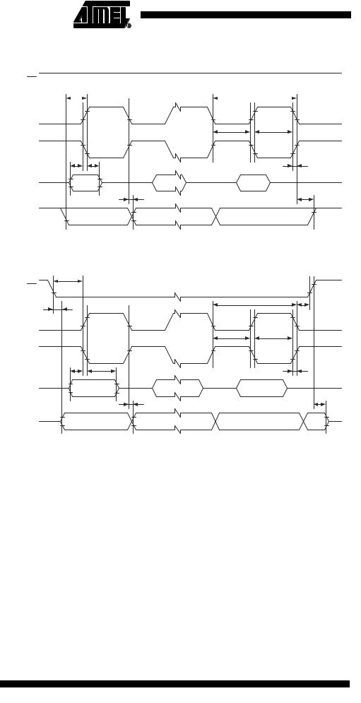
Figure 146. SPI Interface Timing Requirements (Master Mode)
SS
6 |
|
1 |
SCK |
|
|
|
|
(CPOL = 0) |
|
|
|
|
|
|
2 |
2 |
|
SCK |
|
|
|
|
(CPOL = 1) |
|
|
|
|
4 |
5 |
|
3 |
|
MISO |
MSB |
... |
LSB |
|
(Data Input) |
||||
|
|
|
||
|
|
7 |
8 |
|
MOSI |
MSB |
... |
LSB |
|
(Data Output) |
||||
|
|
|
Figure 147. SPI Interface Timing Requirements (Slave Mode)
18 |
|
|
|
|
|
SS |
|
|
|
|
|
9 |
|
|
10 |
16 |
|
|
|
|
|
||
SCK |
|
|
|
|
|
(CPOL = 0) |
|
|
|
|
|
|
|
11 |
11 |
|
|
SCK |
|
|
|
|
|
(CPOL = 1) |
|
|
|
|
|
13 |
14 |
|
|
12 |
|
MOSI |
MSB |
... |
LSB |
|
|
(Data Input) |
|
||||
|
|
|
|
||
|
|
15 |
|
17 |
|
MISO |
MSB |
... |
LSB |
X |
|
(Data Output) |
|||||
|
|
|
|
290 ATmega32(L)
2503F–AVR–12/03