

 ATmega32(L)
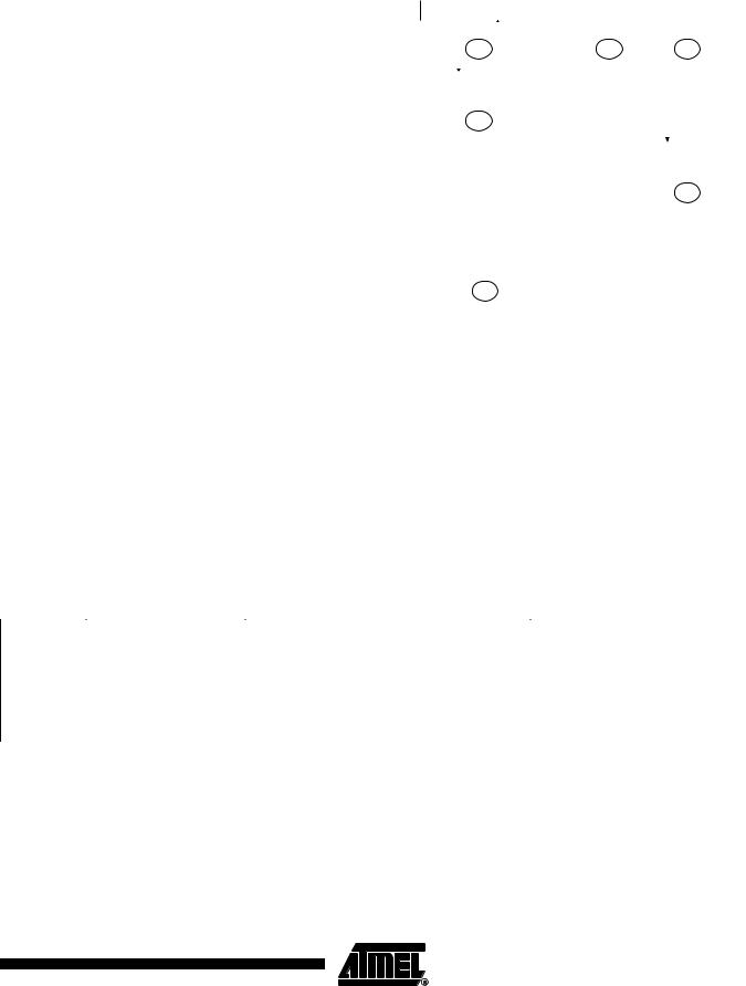
Figure 93. Formats and States in the Slave Transmitter Mode
|
|
|
Reception of the own |
S |
SLA |
R |
|
A |
|
DATA |
A |
|
DATA |
|
|
|
|
|
|
P or S |
|
|
|
|||
|
|
|
slave address and one or |
|
|
|
|
|
A |
|
|
|
|
|
||||||||||||
|
|
|
more data bytes |
|
|
|
|
|
|
|
|
|
|
|
|
|
|
|
|
|
|
|
|
|
|
|
|
|
|
|
|
|
|
|
|
|
|
|
|
|
|
|
|
|
|
|
|
|
|
|
|
|
|
|
|
|
|
|
|
|
|
|
$A8 |
|
|
$B8 |
|
|
$C0 |
|
|
|
|
|||||||
|
|
|
Arbitration lost as master |
|
|
|
|
|
|
|
|
|
|
|
|
|
|
|
|
|
|
|
|
|
|
|
|
|
|
|
|
|
|
|
|
|
|
|
|
|
|
|
|
|
|
|
|
|
|
|
|
||
|
|
|
|
|
|
|
A |
|
|
|
|
|
|
|
|
|
|
|
|
|
|
|
|
|||
|
|
|
and addressed as slave |
|
|
|
|
|
|
|
|
|
|
|
|
|
|
|
|
|
|
|
|
|||
|
|
|
|
|
|
|
|
|
|
|
|
|
|
|
|
|
|
|
|
|
|
|
|
|
|
|
|
|
|
|
|
|
|
|
|
|
|
|
|
|
|
|
|
|
|
|
|
|
|
|
|
|
|
|
|
|
|
|
|
|
|
|
$B0 |
|
|
|
|
|
|
|
|
|
|
|
|
|
|
|
|
|
|
|
|
Last data byte transmitted. |
|
|
|
|
|
|
|
|
|
|
|
|
|
|
|
|
|
|
|
|
|
|
|
|
|
|
|
|
|
|
|
|
|
|
|
|
|
|
|
|
|
|
|
|
|
|
|
|
||
|
|
|
|
|
|
|
|
|
|
|
|
|
|
|
|
|
A |
|
All 1's |
P or S |
|
|
||||
|
|
|
Switched to not addressed |
|
|
|
|
|
|
|
|
|
|
|
|
|
|
|
|
|||||||
|
|
|
slave (TWEA = '0') |
|
|
|
|
|
|
|
|
|
|
|
|
|
|
|
|
|
|
|
|
|
|
|
|
|
|
|
|
|
|
|
|
|
|
|
|
|
|
|
|
|
|
|
|
|
|
|
|
|
|
|
|
|
|
|
|
|
|
|
|
|
|
|
|
|
|
|
|
$C8 |
|
|
|
|
||||
|
|
|
|
|
|
|
|
|
|
|
|
|
|
|
|
|
|
|
|
|
|
|
|
|||
|
|
|
|
|
|
|
|
|
|
|
|
Any number of data bytes |
|
|
|
|
|
|
|
|
|
|
|
|||
|
|
|
|
From master to slave |
|
DATA |
|
|
A |
|
|
|
|
|
|
|
|
|
|
|
||||||
|
|
|
|
|
|
|
and their associated acknowledge bits |
|
|
|
|
|
|
|
|
|
||||||||||
|
|
|
|
From slave to master |
|
|
|
|
n |
|
This number (contained in TWSR) corresponds |
|
|
|
|
|||||||||||
|
|
|
|
|
|
|
|
|
|
|
|
|
||||||||||||||
|
|
|
|
|
|
|
|
|
|
|
to a defined state of the Two-wire Serial Bus. The |
|
|
|
|
|||||||||||
|
|
|
|
|
|
|
|
|
|
|
|
|
|
|
||||||||||||
|
|
|
|
|
|
|
|
|
|
|
|
prescaler bits are zero or masked to zero |
|
|
|
|
||||||||||
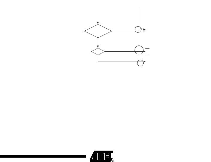
Miscellaneous States |
There are two status codes that do not correspond to a defined TWI state, see Table 78. |
|||||||||||||||||||||||||
Status $F8 indicates that no relevant information is available because the TWINT Flag is not set. This occurs between other states, and when the TWI is not involved in a serial transfer.
Status $00 indicates that a bus error has occurred during a Two-wire Serial Bus transfer. A bus error occurs when a START or STOP condition occurs at an illegal position in the format frame. Examples of such illegal positions are during the serial transfer of an address byte, a data byte, or an acknowledge bit. When a bus error occurs, TWINT is set. To recover from a bus error, the TWSTO Flag must set and TWINT must be cleared by writing a logic one to it. This causes the TWI to enter the not addressed slave mode and to clear the TWSTO Flag (no other bits in TWCR are affected). The SDA and SCL lines are released, and no STOP condition is transmitted.
Table 78. |
Miscellaneous States |
|
|
|
|
|
|
||
Status Code |
|
|
|
Application Software Response |
|
|
|||
(TWSR) |
|
Status of the Two-wire Serial |
|
|
To TWCR |
|
|
||
Prescaler Bits |
|
Bus and Two-wire |
Serial Inter- |
|
|
|
|
||
|
To/from TWDR |
STA |
STO |
TWINT |
TWEA |
|
|||
are 0 |
|
face Hardware |
|
Next Action Taken by TWI Hardware |
|||||
|
|
|
|||||||
|
|
|
|
|
|
|
|||
$F8 |
|
No relevant state |
information |
No TWDR action |
|
No TWCR action |
|
Wait or proceed current transfer |
|
|
|
available; TWINT = “0” |
|
|
|
|
|
|
|
$00 |
|
Bus error due to an illegal |
No TWDR action |
0 |
1 |
1 |
X |
Only the internal hardware is affected, no STOP condi- |
|
|
|
START or STOP condition |
|
|
|
|
|
tion is sent on the bus. In all cases, the bus is released |
|
|
|
|
|
|
|
|
|
|
and TWSTO is cleared. |
193
2503F–AVR–12/03
 ATmega32(L)