- •Features
- •Pin Configurations
- •Disclaimer
- •Overview
- •Block Diagram
- •Pin Descriptions
- •Port A (PA7..PA0)
- •Port B (PB7..PB0)
- •Port C (PC7..PC0)
- •Port D (PD7..PD0)
- •RESET
- •XTAL1
- •XTAL2
- •AVCC
- •AREF
- •AVR CPU Core
- •Introduction
- •Architectural Overview
- •Status Register
- •Stack Pointer
- •Interrupt Response Time
- •SRAM Data Memory
- •Data Memory Access Times
- •EEPROM Data Memory
- •EEPROM Read/Write Access
- •I/O Memory
- •Clock Systems and their Distribution
- •CPU Clock – clkCPU
- •I/O Clock – clkI/O
- •Flash Clock – clkFLASH
- •ADC Clock – clkADC
- •Clock Sources
- •Default Clock Source
- •Crystal Oscillator
- •External RC Oscillator
- •External Clock
- •Timer/Counter Oscillator
- •Idle Mode
- •Power-down Mode
- •Power-save Mode
- •Standby Mode
- •Extended Standby Mode
- •Analog to Digital Converter
- •Analog Comparator
- •Brown-out Detector
- •Internal Voltage Reference
- •Watchdog Timer
- •Port Pins
- •Resetting the AVR
- •Reset Sources
- •Power-on Reset
- •External Reset
- •Brown-out Detection
- •Watchdog Reset
- •Watchdog Timer
- •Interrupts
- •I/O Ports
- •Introduction
- •Configuring the Pin
- •Reading the Pin Value
- •Unconnected pins
- •Alternate Port Functions
- •Alternate Functions of Port A
- •Alternate Functions of Port B
- •Alternate Functions of Port C
- •Alternate Functions of Port D
- •Port A Data Register – PORTA
- •Port B Data Register – PORTB
- •Port C Data Register – PORTC
- •Port D Data Register – PORTD
- •External Interrupts
- •8-bit Timer/Counter0 with PWM
- •Overview
- •Registers
- •Definitions
- •Counter Unit
- •Output Compare Unit
- •Force Output Compare
- •Modes of Operation
- •Normal Mode
- •Fast PWM Mode
- •Phase Correct PWM Mode
- •Internal Clock Source
- •Prescaler Reset
- •External Clock Source
- •16-bit Timer/Counter1
- •Overview
- •Registers
- •Definitions
- •Compatibility
- •Counter Unit
- •Input Capture Unit
- •Input Capture Trigger Source
- •Noise Canceler
- •Using the Input Capture Unit
- •Output Compare Units
- •Force Output Compare
- •Modes of Operation
- •Normal Mode
- •Fast PWM Mode
- •Phase Correct PWM Mode
- •8-bit Timer/Counter2 with PWM and Asynchronous Operation
- •Overview
- •Registers
- •Definitions
- •Counter Unit
- •Output Compare Unit
- •Force Output Compare
- •Modes of Operation
- •Normal Mode
- •Fast PWM Mode
- •Phase Correct PWM Mode
- •Timer/Counter Prescaler
- •SS Pin Functionality
- •Slave Mode
- •Master Mode
- •SPI Control Register – SPCR
- •SPI Status Register – SPSR
- •SPI Data Register – SPDR
- •Data Modes
- •USART
- •Overview
- •AVR USART vs. AVR UART – Compatibility
- •Clock Generation
- •External Clock
- •Synchronous Clock Operation
- •Frame Formats
- •Parity Bit Calculation
- •USART Initialization
- •Parity Generator
- •Disabling the Transmitter
- •Receiver Error Flags
- •Parity Checker
- •Disabling the Receiver
- •Flushing the Receive Buffer
- •Asynchronous Data Recovery
- •Using MPCM
- •Write Access
- •Read Access
- •Two-wire Serial Interface
- •Features
- •TWI Terminology
- •Electrical Interconnection
- •Transferring Bits
- •START and STOP Conditions
- •Address Packet Format
- •Data Packet Format
- •Overview of the TWI Module
- •SCL and SDA Pins
- •Bit Rate Generator Unit
- •Bus Interface Unit
- •Address Match Unit
- •Control Unit
- •TWI Register Description
- •TWI Bit Rate Register – TWBR
- •TWI Control Register – TWCR
- •TWI Status Register – TWSR
- •TWI Data Register – TWDR
- •Using the TWI
- •Transmission Modes
- •Master Transmitter Mode
- •Master Receiver Mode
- •Slave Receiver Mode
- •Slave Transmitter Mode
- •Miscellaneous States
- •Analog Comparator
- •Analog Comparator Multiplexed Input
- •Features
- •Operation
- •Starting a Conversion
- •Differential Gain Channels
- •Changing Channel or Reference Selection
- •ADC Input Channels
- •ADC Voltage Reference
- •ADC Noise Canceler
- •Analog Input Circuitry
- •ADC Accuracy Definitions
- •ADC Conversion Result
- •ADLAR = 0
- •ADLAR = 1
- •Features
- •Overview
- •Test Access Port – TAP
- •TAP Controller
- •PRIVATE0; $8
- •PRIVATE1; $9
- •PRIVATE2; $A
- •PRIVATE3; $B
- •Bibliography
- •Features
- •System Overview
- •Data Registers
- •Bypass Register
- •Device Identification Register
- •Reset Register
- •Boundary-scan Chain
- •EXTEST; $0
- •IDCODE; $1
- •SAMPLE_PRELOAD; $2
- •AVR_RESET; $C
- •BYPASS; $F
- •Scanning the Digital Port Pins
- •Scanning the RESET Pin
- •Scanning the Clock Pins
- •Scanning the ADC
- •Features
- •Application Section
- •BLS – Boot Loader Section
- •Read-While-Write and no Read-While-Write Flash Sections
- •Boot Loader Lock Bits
- •Performing a Page Write
- •Using the SPM Interrupt
- •Setting the Boot Loader Lock Bits by SPM
- •Reading the Fuse and Lock Bits from Software
- •Preventing Flash Corruption
- •Fuse Bits
- •Latching of Fuses
- •Signature Bytes
- •Calibration Byte
- •Signal Names
- •Parallel Programming
- •Enter Programming Mode
- •Chip Erase
- •Programming the Flash
- •Programming the EEPROM
- •Reading the Flash
- •Reading the EEPROM
- •Programming the Lock Bits
- •Reading the Signature Bytes
- •Reading the Calibration Byte
- •SPI Serial Downloading
- •Data Polling Flash
- •Data Polling EEPROM
- •AVR_RESET ($C)
- •PROG_ENABLE ($4)
- •PROG_COMMANDS ($5)
- •PROG_PAGELOAD ($6)
- •PROG_PAGEREAD ($7)
- •Data Registers
- •Reset Register
- •Programming Enable Register
- •Virtual Flash Page Read Register
- •Programming Algorithm
- •Entering Programming Mode
- •Leaving Programming Mode
- •Performing Chip Erase
- •Programming the Flash
- •Reading the Flash
- •Programming the EEPROM
- •Reading the EEPROM
- •Programming the Fuses
- •Programming the Lock Bits
- •Reading the Signature Bytes
- •Reading the Calibration Byte
- •Electrical Characteristics
- •Absolute Maximum Ratings*
- •DC Characteristics
- •External Clock Drive Waveforms
- •External Clock Drive
- •Two-wire Serial Interface Characteristics
- •ADC Characteristics
- •Register Summary
- •Instruction Set Summary
- •Ordering Information
- •Packaging Information
- •Errata
- •ATmega32 Rev. A
- •Datasheet Change Log for ATmega32
- •Changes from Rev. 2503E-09/03 to Rev. 2503F-12/03
- •Changes from Rev. 2503D-02/03 to Rev. 2503E-09/03
- •Changes from Rev. 2503C-10/02 to Rev. 2503D-02/03
- •Changes from Rev. 2503B-10/02 to Rev. 2503C-10/02
- •Changes from Rev. 2503A-03/02 to Rev. 2503B-10/02
- •Table of Contents
Figure 71. Synchronous Mode XCK Timing.
|
|
UCPOL = 1 |
XCK |
|||||||||||
|
|
|
|
RxD / TxD |
||||||||||
|
|
|
|
|
|
|
|
|
|
Sample |
||||
|
|
|
|
|
|
|
|
|
||||||
|
|
|
|
|
|
|
|
|
|
|||||
|
|
|
|
|
|
|
|
|
|
|
|
|||
|
|
UCPOL = 0 |
XCK |
|||||||||||
|
|
|
|
|
|
|
|
|
|
|
|
|
|
|
|
|
|
|
RxD / TxD |
||||||||||
|
|
|
|
|
|
|
|
|
|
Sample |
||||
|
|
|
|
|
|
|
|
|
|
|||||
|
|
|
|
|
|
|
|
|
|
|||||
|
|
|
|
|
|
|
|
|
|
|||||
|
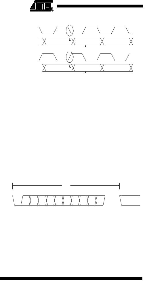
The UCPOL bit UCRSC selects which XCK clock edge is used for data sampling and |
|||||||||||||
|
which is used for data change. As Figure 71 shows, when UCPOL is zero the data will |
|||||||||||||
|
be changed at rising XCK edge and sampled at falling XCK edge. If UCPOL is set, the |
|||||||||||||
|
data will be changed at falling XCK edge and sampled at rising XCK edge. |
|||||||||||||
Frame Formats |
A serial frame is defined to be one character of data bits with synchronization bits (start |
|||||||||||||
|
and stop bits), and optionally a parity bit for error checking. The USART accepts all 30 |
|||||||||||||
|
combinations of the following as valid frame formats: |
|||||||||||||
|
• 1 start bit |
|
|
|
|
|
|
|
|
|
|
|
||
|
• 5, 6, 7, 8, or 9 data bits |
|||||||||||||
|
• no, even or odd parity bit |
|||||||||||||
|
• 1 or 2 stop bits |
|||||||||||||
|
A frame starts with the start bit followed by the least significant data bit. Then the next |
|||||||||||||
|
data bits, up to a total of nine, are succeeding, ending with the most significant bit. If |
|||||||||||||
|
enabled, the parity bit is inserted after the data bits, before the stop bits. When a com- |
|||||||||||||
|
plete frame is transmitted, it can be directly followed by a new frame, or the |
|||||||||||||
|
communication line can be set to an idle (high) state. Figure 72 illustrates the possible |
|||||||||||||
|
combinations of the frame formats. Bits inside brackets are optional. |
|||||||||||||
|
Figure 72. |
Frame Formats |
||||||||||||
|
|
|
|
|
|
|
|
|||||||
|
|
|
|
|
|
|
FRAME |
|
||||||
|
|
|
|
|
|
|
||||||||
|
|
|
|
|
|
|
|
|
|
|
|
|
|
|
|
|
(IDLE) |
St |
0 1 2 3 4 [5] [6] [7] [8] [P] Sp1 [Sp2] (St / IDLE) |
St Start bit, always low.
(n)Data bits (0 to 8).
P Parity bit. Can be odd or even.
Sp Stop bit, always high.
IDLE No transfers on the communication line (RxD or TxD). An IDLE line must be high.
The frame format used by the USART is set by the UCSZ2:0, UPM1:0, and USBS bits in UCSRB and UCSRC. The Receiver and Transmitter use the same setting. Note that changing the setting of any of these bits will corrupt all ongoing communication for both the Receiver and Transmitter.
142 ATmega32(L)
2503F–AVR–12/03
ATmega32(L)
The USART Character SiZe (UCSZ2:0) bits select the number of data bits in the frame. The USART Parity mode (UPM1:0) bits enable and set the type of parity bit. The selection between one or two stop bits is done by the USART Stop Bit Select (USBS) bit. The receiver ignores the second stop bit. An FE (Frame Error) will therefore only be detected
|
in the cases where the first stop bit is zero. |
|
|
|
|
|||
Parity Bit Calculation |
The parity bit is calculated by doing an exclusive-or of all the data bits. If odd parity is |
|||||||
|
used, the result of the exclusive or is inverted. The relation between the parity bit and |
|||||||
|
data bits is as follows:: |
… |
d |
|
d2 |
d1 d0 |
|
|
|
|
Pev en = dn – 1 |
3 |
0 |
||||
|
|
Pod d = dn – 1 |
… |
d |
3 |
d2 |
d1 d0 |
1 |
|
Peven |
Parity bit using even parity |
|
|
|
|
|
|
|
Podd |
Parity bit using odd parity |
|
|
|
|
|
|
|
dn |
Data bit n of the character |
|
|
|
|
|
|
|
If used, the parity bit is located between the last data bit and first stop bit of a serial |
|||||||
|
frame. |
|
|
|
|
|
|
|
143
2503F–AVR–12/03