

- •Features
- •Pin Configurations
- •Disclaimer
- •Overview
- •Block Diagram
- •Pin Descriptions
- •Port A (PA7..PA0)
- •Port B (PB7..PB0)
- •Port C (PC7..PC0)
- •Port D (PD7..PD0)
- •RESET
- •XTAL1
- •XTAL2
- •AVCC
- •AREF
- •AVR CPU Core
- •Introduction
- •Architectural Overview
- •Status Register
- •Stack Pointer
- •Interrupt Response Time
- •SRAM Data Memory
- •Data Memory Access Times
- •EEPROM Data Memory
- •EEPROM Read/Write Access
- •I/O Memory
- •Clock Systems and their Distribution
- •CPU Clock – clkCPU
- •I/O Clock – clkI/O
- •Flash Clock – clkFLASH
- •ADC Clock – clkADC
- •Clock Sources
- •Default Clock Source
- •Crystal Oscillator
- •External RC Oscillator
- •External Clock
- •Timer/Counter Oscillator
- •Idle Mode
- •Power-down Mode
- •Power-save Mode
- •Standby Mode
- •Extended Standby Mode
- •Analog to Digital Converter
- •Analog Comparator
- •Brown-out Detector
- •Internal Voltage Reference
- •Watchdog Timer
- •Port Pins
- •Resetting the AVR
- •Reset Sources
- •Power-on Reset
- •External Reset
- •Brown-out Detection
- •Watchdog Reset
- •Watchdog Timer
- •Interrupts
- •I/O Ports
- •Introduction
- •Configuring the Pin
- •Reading the Pin Value
- •Unconnected pins
- •Alternate Port Functions
- •Alternate Functions of Port A
- •Alternate Functions of Port B
- •Alternate Functions of Port C
- •Alternate Functions of Port D
- •Port A Data Register – PORTA
- •Port B Data Register – PORTB
- •Port C Data Register – PORTC
- •Port D Data Register – PORTD
- •External Interrupts
- •8-bit Timer/Counter0 with PWM
- •Overview
- •Registers
- •Definitions
- •Counter Unit
- •Output Compare Unit
- •Force Output Compare
- •Modes of Operation
- •Normal Mode
- •Fast PWM Mode
- •Phase Correct PWM Mode
- •Internal Clock Source
- •Prescaler Reset
- •External Clock Source
- •16-bit Timer/Counter1
- •Overview
- •Registers
- •Definitions
- •Compatibility
- •Counter Unit
- •Input Capture Unit
- •Input Capture Trigger Source
- •Noise Canceler
- •Using the Input Capture Unit
- •Output Compare Units
- •Force Output Compare
- •Modes of Operation
- •Normal Mode
- •Fast PWM Mode
- •Phase Correct PWM Mode
- •8-bit Timer/Counter2 with PWM and Asynchronous Operation
- •Overview
- •Registers
- •Definitions
- •Counter Unit
- •Output Compare Unit
- •Force Output Compare
- •Modes of Operation
- •Normal Mode
- •Fast PWM Mode
- •Phase Correct PWM Mode
- •Timer/Counter Prescaler
- •SS Pin Functionality
- •Slave Mode
- •Master Mode
- •SPI Control Register – SPCR
- •SPI Status Register – SPSR
- •SPI Data Register – SPDR
- •Data Modes
- •USART
- •Overview
- •AVR USART vs. AVR UART – Compatibility
- •Clock Generation
- •External Clock
- •Synchronous Clock Operation
- •Frame Formats
- •Parity Bit Calculation
- •USART Initialization
- •Parity Generator
- •Disabling the Transmitter
- •Receiver Error Flags
- •Parity Checker
- •Disabling the Receiver
- •Flushing the Receive Buffer
- •Asynchronous Data Recovery
- •Using MPCM
- •Write Access
- •Read Access
- •Two-wire Serial Interface
- •Features
- •TWI Terminology
- •Electrical Interconnection
- •Transferring Bits
- •START and STOP Conditions
- •Address Packet Format
- •Data Packet Format
- •Overview of the TWI Module
- •SCL and SDA Pins
- •Bit Rate Generator Unit
- •Bus Interface Unit
- •Address Match Unit
- •Control Unit
- •TWI Register Description
- •TWI Bit Rate Register – TWBR
- •TWI Control Register – TWCR
- •TWI Status Register – TWSR
- •TWI Data Register – TWDR
- •Using the TWI
- •Transmission Modes
- •Master Transmitter Mode
- •Master Receiver Mode
- •Slave Receiver Mode
- •Slave Transmitter Mode
- •Miscellaneous States
- •Analog Comparator
- •Analog Comparator Multiplexed Input
- •Features
- •Operation
- •Starting a Conversion
- •Differential Gain Channels
- •Changing Channel or Reference Selection
- •ADC Input Channels
- •ADC Voltage Reference
- •ADC Noise Canceler
- •Analog Input Circuitry
- •ADC Accuracy Definitions
- •ADC Conversion Result
- •ADLAR = 0
- •ADLAR = 1
- •Features
- •Overview
- •Test Access Port – TAP
- •TAP Controller
- •PRIVATE0; $8
- •PRIVATE1; $9
- •PRIVATE2; $A
- •PRIVATE3; $B
- •Bibliography
- •Features
- •System Overview
- •Data Registers
- •Bypass Register
- •Device Identification Register
- •Reset Register
- •Boundary-scan Chain
- •EXTEST; $0
- •IDCODE; $1
- •SAMPLE_PRELOAD; $2
- •AVR_RESET; $C
- •BYPASS; $F
- •Scanning the Digital Port Pins
- •Scanning the RESET Pin
- •Scanning the Clock Pins
- •Scanning the ADC
- •Features
- •Application Section
- •BLS – Boot Loader Section
- •Read-While-Write and no Read-While-Write Flash Sections
- •Boot Loader Lock Bits
- •Performing a Page Write
- •Using the SPM Interrupt
- •Setting the Boot Loader Lock Bits by SPM
- •Reading the Fuse and Lock Bits from Software
- •Preventing Flash Corruption
- •Fuse Bits
- •Latching of Fuses
- •Signature Bytes
- •Calibration Byte
- •Signal Names
- •Parallel Programming
- •Enter Programming Mode
- •Chip Erase
- •Programming the Flash
- •Programming the EEPROM
- •Reading the Flash
- •Reading the EEPROM
- •Programming the Lock Bits
- •Reading the Signature Bytes
- •Reading the Calibration Byte
- •SPI Serial Downloading
- •Data Polling Flash
- •Data Polling EEPROM
- •AVR_RESET ($C)
- •PROG_ENABLE ($4)
- •PROG_COMMANDS ($5)
- •PROG_PAGELOAD ($6)
- •PROG_PAGEREAD ($7)
- •Data Registers
- •Reset Register
- •Programming Enable Register
- •Virtual Flash Page Read Register
- •Programming Algorithm
- •Entering Programming Mode
- •Leaving Programming Mode
- •Performing Chip Erase
- •Programming the Flash
- •Reading the Flash
- •Programming the EEPROM
- •Reading the EEPROM
- •Programming the Fuses
- •Programming the Lock Bits
- •Reading the Signature Bytes
- •Reading the Calibration Byte
- •Electrical Characteristics
- •Absolute Maximum Ratings*
- •DC Characteristics
- •External Clock Drive Waveforms
- •External Clock Drive
- •Two-wire Serial Interface Characteristics
- •ADC Characteristics
- •Register Summary
- •Instruction Set Summary
- •Ordering Information
- •Packaging Information
- •Errata
- •ATmega32 Rev. A
- •Datasheet Change Log for ATmega32
- •Changes from Rev. 2503E-09/03 to Rev. 2503F-12/03
- •Changes from Rev. 2503D-02/03 to Rev. 2503E-09/03
- •Changes from Rev. 2503C-10/02 to Rev. 2503D-02/03
- •Changes from Rev. 2503B-10/02 to Rev. 2503C-10/02
- •Changes from Rev. 2503A-03/02 to Rev. 2503B-10/02
- •Table of Contents
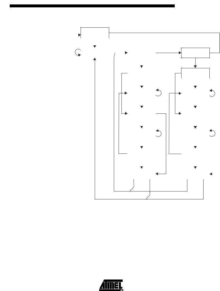
Figure 113. TAP Controller State Diagram
1  Test-Logic-Reset
|
|
0 |
|
|
|
|
|
|
0 |
|
|
1 |
|
|
|
|
1 |
Run-Test/Idle |
|
Select-DR Scan |
||||||
|
|
|
|
|||||
|
|
|
|
|
|
|
|
|
|
|
|
|
|
|
0 |
|
|
|
|
|
|
1 |
|
|
|
|
|
|
|
|
|
|
|
|
|
|
|
|
|
Capture-DR |
|
|
||
|
|
|
|
|
|
|
||
|
|
|
|
|
|
|
|
|
|
|
|
|
|
|
0 |
|
|
|
|
|
|
|
|
|
|
|
|
|
|
|
|
|
|
|
|
|
|
|
|
|
Shift-DR |
|
0 |
|
|
|
|
|
|
|
|
|
|
|
|
|
|
|
|
1 |
|
|
|
|
|
|
|
|
|
|
1 |
|
|
|
|
|
Exit1-DR |
|
||
|
|
|
|
|
|
|
||
|
|
|
|
|
|
|
|
|
|
|
|
|
|
|
0 |
|
|
|
|
|
|
|
|
|
|
|
|
|
|
|
|
|
|
|
|
|
|
|
|
|
Pause-DR |
|
0 |
|
|
|
|
|
|
|
|
|
|
|
|
|
|
|
|
1 |
|
|
|
|
|
|
0 |
|
|
|
|
|
|
|
|
|
|
|
|
|
|
|
|
|
Exit2-DR |
|
|
||
|
|
|
|
|
|
|
||
|
|
|
|
|
|
|
|
|
|
|
|
|
|
|
1 |
|
|
|
|
|
|
|
|
|
|
|
|
|
|
|
|
|
|
|
|
|
|
|
|
|
Update-DR |
|
|
|
|
|
|
|
|
|
|
|
|
|
|
|
|
|
1 |
|
0 |
|
ATmega32(L)
1
Select-IR Scan
0
1 |
Capture-IR |
|
|
|
0 |
|
|
|
|
|
|
|
|
|
|
|
|
|
Shift-IR |
|
0 |
|
|
|
|
|
|
|
|
1 |
|
|
|
|
|
|
|
|
|
|
|
1 |
|
Exit1-IR |
|
||
|
|
|
||
|
|
|
|
|
|
|
0 |
|
|
|
|
|
|
|
|
|
|
|
0 |
|
Pause-IR |
|
||
|
|
|
|
|
|
|
1 |
|
|
0 |
|
|
|
|
Exit2-IR |
|
|
||
|
|
|
||
|
|
|
|
|
|
|
1 |
|
|
|
|
|
|
|
|
|
|
|
|
|
Update-IR |
|
|
|
|
|
|
||
|
|
|
|
|
|
1 |
|
0 |
|
TAP Controller |
The TAP controller is a 16-state finite state machine that controls the operation of the |
||||
|
Boundary-scan circuitry, JTAG programming circuitry, or On-chip Debug system. The |
||||
|
state transitions depicted in Figure 113 depend on the signal present on TMS (shown |
||||
|
adjacent to each state transition) at the time of the rising edge at TCK. The initial state |
||||
|
after a Power-On Reset is Test-Logic-Reset. |
||||
|
As a definition in this document, the LSB is shifted in and out first for all Shift Registers. |
||||
|
Assuming Run-Test/Idle is the present state, a typical scenario for using the JTAG inter- |
||||
|
face is: |
||||
|
• At the TMS input, apply the sequence 1, 1, 0, 0 at the rising edges of TCK to enter |
||||
|
the Shift Instruction Register – Shift-IR state. While in this state, shift the four bits of |
||||
|
the JTAG instructions into the JTAG Instruction Register from the TDI input at the |
||||
|
rising edge of TCK. The TMS input must be held low during input of the 3 LSBs in |
||||
|
order to remain in the Shift-IR state. The MSB of the instruction is shifted in when |
||||
|
|
|
|
|
|
|
|
|
|
|
219 |
2503F–AVR–12/03 |
|
|
|
|
|
|
|
|
|
|
|

Using the Boundaryscan Chain
Using the On-chip Debug
System
this state is left by setting TMS high. While the instruction is shifted in from the TDI pin, the captured IR-state 0x01 is shifted out on the TDO pin. The JTAG Instruction selects a particular Data Register as path between TDI and TDO and controls the circuitry surrounding the selected Data Register.
•Apply the TMS sequence 1, 1, 0 to re-enter the Run-Test/Idle state. The instruction is latched onto the parallel output from the Shift Register path in the Update-IR state. The Exit-IR, Pause-IR, and Exit2-IR states are only used for navigating the state machine.
•At the TMS input, apply the sequence 1, 0, 0 at the rising edges of TCK to enter the Shift Data Register – Shift-DR state. While in this state, upload the selected Data Register (selected by the present JTAG instruction in the JTAG Instruction Register) from the TDI input at the rising edge of TCK. In order to remain in the Shift-DR state, the TMS input must be held low during input of all bits except the MSB. The MSB of the data is shifted in when this state is left by setting TMS high. While the Data Register is shifted in from the TDI pin, the parallel inputs to the Data Register captured in the Capture-DR state is shifted out on the TDO pin.
•Apply the TMS sequence 1, 1, 0 to re-enter the Run-Test/Idle state. If the selected Data Register has a latched parallel-output, the latching takes place in the UpdateDR state. The Exit-DR, Pause-DR, and Exit2-DR states are only used for navigating the state machine.
As shown in the state diagram, the Run-Test/Idle state need not be entered between selecting JTAG instruction and using Data Registers, and some JTAG instructions may select certain functions to be performed in the Run-Test/Idle, making it unsuitable as an Idle state.
Note: Independent of the initial state of the TAP Controller, the Test-Logic-Reset state can always be entered by holding TMS high for five TCK clock periods.
For detailed information on the JTAG specification, refer to the literature listed in “Bibliography” on page 222.
A complete description of the Boundary-scan capabilities are given in the section “IEEE 1149.1 (JTAG) Boundary-scan” on page 223.
As shown in Figure 112, the hardware support for On-chip Debugging consists mainly of:
•A scan chain on the interface between the internal AVR CPU and the internal peripheral units
•Break Point unit
•Communication interface between the CPU and JTAG system
All read or modify/write operations needed for implementing the Debugger are done by applying AVR instructions via the internal AVR CPU Scan Chain. The CPU sends the result to an I/O memory mapped location which is part of the communication interface between the CPU and the JTAG system.
The Break Point Unit implements Break on Change of Program Flow, Single Step
Break, 2 Program Memory Break Points, and 2 combined Break Points. Together, the 4
Break Points can be configured as either:
•4 single Program Memory Break Points
•3 Single Program Memory Break Point + 1 single Data Memory Break Point
•2 single Program Memory Break Points + 2 single Data Memory Break Points
220 ATmega32(L)
2503F–AVR–12/03
 ATmega32(L)
On-chip Debug Specific
JTAG Instructions
•2 single Program Memory Break Points + 1 Program Memory Break Point with mask (“range Break Point”)
•2 single Program Memory Break Points + 1 Data Memory Break Point with mask (“range Break Point”)
A debugger, like the AVR Studio, may however use one or more of these resources for its internal purpose, leaving less flexibility to the end-user.
A list of the On-chip Debug specific JTAG instructions is given in “On-chip Debug Specific JTAG Instructions” on page 221.
The JTAGEN Fuse must be programmed to enable the JTAG Test Access Port. In addition, the OCDEN Fuse must be programmed and no Lock bits must be set for the Onchip Debug system to work. As a security feature, the On-chip Debug system is disabled when any Lock bits are set. Otherwise, the On-chip Debug system would have provided a back-door into a secured device.
The AVR JTAG ICE from Atmel is a powerful development tool for On-chip Debugging of all AVR 8-bit RISC Microcontrollers with IEEE 1149.1 compliant JTAG interface. The JTAG ICE and the AVR Studio user interface give the user complete control of the internal resources of the microcontroller, helping to reduce development time by making debugging easier. The JTAG ICE performs real-time emulation of the micrcontroller while it is running in a target system.
Please refer to the Support Tools section on the AVR pages on www.atmel.com for a full description of the AVR JTEG ICE. AVR Studio can be downloaded free from Software section on the same web site.
All necessary execution commands are available in AVR Studio, both on source level and on disassembly level. The user can execute the program, single step through the code either by tracing into or stepping over functions, step out of functions, place the cursor on a statement and execute until the statement is reached, stop the execution, and reset the execution target. In addition, the user can have an unlimited number of code breakpoints (using the BREAK instruction) and up to two data memory breakpoints, alternatively combined as a mask (range) Break Point.
The On-chip Debug support is considered being private JTAG instructions, and distributed within ATMEL and to selected third party vendors only. Instruction opcodes are listed for reference.
PRIVATE0; $8 |
Private JTAG instruction for accessing On-chip Debug system. |
PRIVATE1; $9 |
Private JTAG instruction for accessing On-chip Debug system. |
PRIVATE2; $A |
Private JTAG instruction for accessing On-chip Debug system. |
PRIVATE3; $B |
Private JTAG instruction for accessing On-chip Debug system. |
221
2503F–AVR–12/03

On-chip Debug Related
Register in I/O Memory
On-chip Debug Register –
OCDR
Using the JTAG
Programming
Capabilities
Bibliography
|
|
|
|
|
|
|
|
|
|
|
|
|
|
|
|
|
|
|
|
|
|
|
|
|
|
|
|
Bit |
7 |
6 |
5 |
4 |
3 |
2 |
1 |
0 |
|
||||
|
|
|
|
|
|
|
|
|
|
|
|
|
OCDR |
|
MSB/IDRD |
|
|
|
|
|
|
|
|
|
|
LSB |
|
|
|
|
|
|
|
|
|
|
|
|
|
|
|
Read/Write |
R/W |
R/W |
|
|
|
R/W |
|
R/W |
R/W |
R/W |
R/W |
R/W |
|
Initial Value |
0 |
0 |
0 |
0 |
0 |
0 |
0 |
0 |
|
||||
The OCDR Register provides a communication channel from the running program in the microcontroller to the debugger. The CPU can transfer a byte to the debugger by writing to this location. At the same time, an Internal Flag; I/O Debug Register Dirty – IDRD – is set to indicate to the debugger that the register has been written. When the CPU reads the OCDR Register the 7 LSB will be from the OCDR Register, while the MSB is the IDRD bit. The debugger clears the IDRD bit when it has read the information.
In some AVR devices, this register is shared with a standard I/O location. In this case, the OCDR Register can only be accessed if the OCDEN Fuse is programmed, and the debugger enables access to the OCDR Register. In all other cases, the standard I/O location is accessed.
Refer to the debugger documentation for further information on how to use this register.
Programming of AVR parts via JTAG is performed via the 4-pin JTAG port, TCK, TMS, TDI and TDO. These are the only pins that need to be controlled/observed to perform JTAG programming (in addition to power pins). It is not required to apply 12V externally. The JTAGEN fuse must be programmed and the JTD bit in the MCUSR Register must be cleared to enable the JTAG Test Access Port.
The JTAG programming capability supports:
•Flash programming and verifying
•EEPROM programming and verifying
•Fuse programming and verifying
•Lock bit programming and verifying
The Lock bit security is exactly as in Parallel Programming mode. If the Lock bits LB1 or LB2 are programmed, the OCDEN Fuse cannot be programmed unless first doing a chip erase. This is a security feature that ensures no back-door exists for reading out the content of a secured device.
The details on programming through the JTAG interface and programming specific JTAG instructions are given in the section “Programming via the JTAG Interface” on page 272.
For more information about general Boundary-scan, the following literature can be consulted:
•IEEE: IEEE Std 1149.1-1990. IEEE Standard Test Access Port and Boundary-scan Architecture, IEEE, 1993
•Colin Maunder: The Board Designers Guide to Testable Logic Circuits, AddisonWesley, 1992
222 ATmega32(L)
2503F–AVR–12/03