


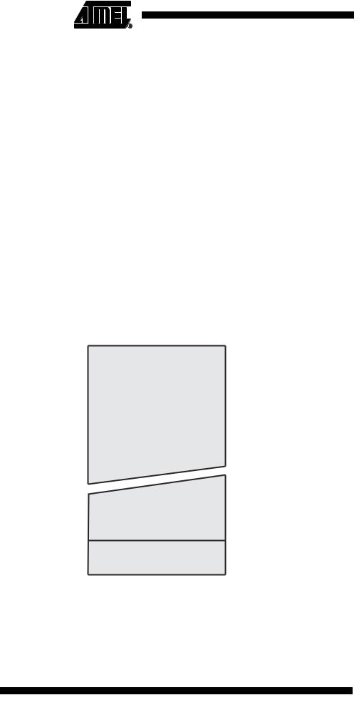
The X-register, Y-register and The registers R26..R31 have some added functions to their general purpose usage. Z-register These registers are 16-bit address pointers for indirect addressing of the Data Space.
The three indirect address registers X, Y, and Z are defined as described in Figure 5.
Figure 5. The X-, Y-, and Z-registers
|
15 |
XH |
|
XL |
0 |
X - register |
7 |
|
0 |
7 |
0 |
|
|
|
|
|
|
|
R27 ($1B) |
|
|
R26 ($1A) |
|
|
15 |
YH |
|
YL |
0 |
|
|
|
|
|
|
Y - register |
7 |
|
0 |
7 |
0 |
|
|
|
|
|
|
|
R29 ($1D) |
|
|
R28 ($1C) |
|
|
15 |
ZH |
|
ZL |
0 |
|
|
|
|
|
|
Z - register |
7 |
0 |
|
7 |
0 |
|
|
|
|
|
|
|
R31 ($1F) |
|
|
R30 ($1E) |
|
In the different addressing modes these address registers have functions as fixed displacement, automatic increment, and automatic decrement (see the Instruction Set Reference for details).
Stack Pointer |
The Stack is mainly used for storing temporary data, for storing local variables and for |
||||||||||
|
storing return addresses after interrupts and subroutine calls. The Stack Pointer Regis- |
||||||||||
|
ter always points to the top of the Stack. Note that the Stack is implemented as growing |
||||||||||
|
from higher memory locations to lower memory locations. This implies that a Stack |
||||||||||
|
PUSH command decreases the Stack Pointer. |
|
|
|
|
|
|||||
|
The Stack Pointer points to the data SRAM Stack area where the Subroutine and Inter- |
||||||||||
|
rupt Stacks are located. This Stack space in the data SRAM must be defined by the |
||||||||||
|
program before any subroutine calls are executed or interrupts are enabled. The Stack |
||||||||||
|
Pointer must be set to point above $60. The Stack Pointer is decremented by one when |
||||||||||
|
data is pushed onto the Stack with the PUSH instruction, and it is decremented by two |
||||||||||
|
when the return address is pushed onto the Stack with subroutine call or interrupt. The |
||||||||||
|
Stack Pointer is incremented by one when data is popped from the Stack with the POP |
||||||||||
|
instruction, and it is incremented by two when data is popped from the Stack with return |
||||||||||
|
from subroutine RET or return from interrupt RETI. |
|
|
|
|
||||||
|
The AVR Stack Pointer is implemented as two 8-bit registers in the I/O space. The num- |
||||||||||
|
ber of bits actually used is implementation dependent. Note that the data space in some |
||||||||||
|
implementations of the AVR architecture is so small that only SPL is needed. In this |
||||||||||
|
case, the SPH Register will not be present. |
|
|
|
|
|
|||||
|
Bit |
15 |
14 |
13 |
12 |
|
11 |
10 |
9 |
8 |
|
|
|
|
|
|
|
|
|
|
|
|
|
|
|
SP15 |
SP14 |
SP13 |
SP12 |
|
SP11 |
SP10 |
SP9 |
SP8 |
SPH |
|
|
|
|
|
|
|
|
|
|
|
SPL |
|
|
SP7 |
SP6 |
SP5 |
SP4 |
|
SP3 |
SP2 |
SP1 |
SP0 |
|
|
|
|
|
|
|
|
|
|
|
|
|
|
|
7 |
6 |
5 |
4 |
|
3 |
2 |
1 |
0 |
|
|
Read/Write |
R/W |
R/W |
R/W |
R/W |
R/W |
R/W |
R/W |
R/W |
|
|
|
|
R/W |
R/W |
R/W |
R/W |
R/W |
R/W |
R/W |
R/W |
|
|
|
Initial Value |
0 |
0 |
0 |
0 |
|
0 |
0 |
0 |
0 |
|
|
|
0 |
0 |
0 |
0 |
|
0 |
0 |
0 |
0 |
|
10 ATmega32(L)
2503F–AVR–12/03
Instruction Execution
Timing
Reset and Interrupt
Handling
2503F–AVR–12/03
ATmega32(L)
This section describes the general access timing concepts for instruction execution. The AVR CPU is driven by the CPU clock clkCPU, directly generated from the selected clock source for the chip. No internal clock division is used.
Figure 6 shows the parallel instruction fetches and instruction executions enabled by the Harvard architecture and the fast-access Register File concept. This is the basic pipelining concept to obtain up to 1 MIPS per MHz with the corresponding unique results for functions per cost, functions per clocks, and functions per power-unit.
Figure 6. The Parallel Instruction Fetches and Instruction Executions
T1 |
T2 |
T3 |
T4 |
clkCPU
1st Instruction Fetch
1st Instruction Execute 2nd Instruction Fetch 2nd Instruction Execute 3rd Instruction Fetch 3rd Instruction Execute 4th Instruction Fetch
Figure 7 shows the internal timing concept for the Register File. In a single clock cycle an ALU operation using two register operands is executed, and the result is stored back to the destination register.
Figure 7. Single Cycle ALU Operation
T1 T2 T3 T4
clkCPU Total Execution Time
Register Operands Fetch
ALU Operation Execute
Result Write Back
The AVR provides several different interrupt sources. These interrupts and the separate reset vector each have a separate program vector in the program memory space. All interrupts are assigned individual enable bits which must be written logic one together with the Global Interrupt Enable bit in the Status Register in order to enable the interrupt. Depending on the Program Counter value, interrupts may be automatically disabled when Boot Lock bits BLB02 or BLB12 are programmed. This feature improves software security. See the section “Memory Programming” on page 254 for details.
The lowest addresses in the program memory space are by default defined as the Reset and Interrupt Vectors. The complete list of vectors is shown in “Interrupts” on page 42. The list also determines the priority levels of the different interrupts. The lower the address the higher is the priority level. RESET has the highest priority, and next is INT0
11

– the External Interrupt Request 0. The Interrupt Vectors can be moved to the start of the Boot Flash section by setting the IVSEL bit in the General Interrupt Control Register (GICR). Refer to “Interrupts” on page 42 for more information. The Reset Vector can also be moved to the start of the boot Flash section by programming the BOOTRST fuse, see “Boot Loader Support – Read-While-Write Self-Programming” on page 242.
When an interrupt occurs, the Global Interrupt Enable I-bit is cleared and all interrupts are disabled. The user software can write logic one to the I-bit to enable nested interrupts. All enabled interrupts can then interrupt the current interrupt routine. The I-bit is automatically set when a Return from Interrupt instruction – RETI – is executed.
There are basically two types of interrupts. The first type is triggered by an event that sets the Interrupt Flag. For these interrupts, the Program Counter is vectored to the actual Interrupt Vector in order to execute the interrupt handling routine, and hardware clears the corresponding Interrupt Flag. Interrupt Flags can also be cleared by writing a logic one to the flag bit position(s) to be cleared. If an interrupt condition occurs while the corresponding interrupt enable bit is cleared, the Interrupt Flag will be set and remembered until the interrupt is enabled, or the flag is cleared by software. Similarly, if one or more interrupt conditions occur while the Global Interrupt Enable bit is cleared, the corresponding Interrupt Flag(s) will be set and remembered until the global interrupt enable bit is set, and will then be executed by order of priority.
The second type of interrupts will trigger as long as the interrupt condition is present. These interrupts do not necessarily have Interrupt Flags. If the interrupt condition disappears before the interrupt is enabled, the interrupt will not be triggered.
When the AVR exits from an interrupt, it will always return to the main program and execute one more instruction before any pending interrupt is served.
Note that the Status Register is not automatically stored when entering an interrupt routine, nor restored when returning from an interrupt routine. This must be handled by software.
When using the CLI instruction to disable interrupts, the interrupts will be immediately disabled. No interrupt will be executed after the CLI instruction, even if it occurs simultaneously with the CLI instruction. The following example shows how this can be used to avoid interrupts during the timed EEPROM write sequence.
Assembly Code Example
in |
r16, SREG |
; store SREG value |
|
cli |
; disable interrupts during timed sequence |
||
sbi |
EECR, |
EEMWE |
; start EEPROM write |
sbi |
EECR, |
EEWE |
|
out SREG, |
r16 |
; restore SREG value (I-bit) |
|
|
|
||
C Code Example |
|
||
|
|
||
char cSREG; |
|
||
cSREG = SREG; |
/* store SREG value */ |
||
/* disable interrupts during timed sequence */
_CLI();
EECR |= (1<<EEMWE); /* start EEPROM write */
EECR |= (1<<EEWE);
SREG = cSREG; /* restore SREG value (I-bit) */
12 ATmega32(L)
2503F–AVR–12/03

 ATmega32(L)
When using the SEI instruction to enable interrupts, the instruction following SEI will be executed before any pending interrupts, as shown in this example.
Assembly Code Example
sei ; set global interrupt enable
sleep ; enter sleep, waiting for interrupt
;note: will enter sleep before any pending
;interrupt(s)
C Code Example
_SEI(); /* set global interrupt enable */
_SLEEP(); /* enter sleep, waiting for interrupt */
/* note: will enter sleep before any pending interrupt(s) */
Interrupt Response Time The interrupt execution response for all the enabled AVR interrupts is four clock cycles minimum. After four clock cycles the program vector address for the actual interrupt handling routine is executed. During this four clock cycle period, the Program Counter is pushed onto the Stack. The vector is normally a jump to the interrupt routine, and this jump takes three clock cycles. If an interrupt occurs during execution of a multi-cycle instruction, this instruction is completed before the interrupt is served. If an interrupt occurs when the MCU is in sleep mode, the interrupt execution response time is increased by four clock cycles. This increase comes in addition to the start-up time from the selected sleep mode.
A return from an interrupt handling routine takes four clock cycles. During these four clock cycles, the Program Counter (two bytes) is popped back from the Stack, the Stack Pointer is incremented by two, and the I-bit in SREG is set.
13
2503F–AVR–12/03
AVR ATmega32
Memories
In-System
Reprogrammable Flash
Program Memory
This section describes the different memories in the ATmega32. The AVR architecture has two main memory spaces, the Data Memory and the Program Memory space. In addition, the ATmega32 features an EEPROM Memory for data storage. All three memory spaces are linear and regular.
The ATmega32 contains 32K bytes On-chip In-System Reprogrammable Flash memory for program storage. Since all AVR instructions are 16 or 32 bits wide, the Flash is organized as 16K x 16. For software security, the Flash Program memory space is divided into two sections, Boot Program section and Application Program section.
The Flash memory has an endurance of at least 10,000 write/erase cycles. The ATmega32 Program Counter (PC) is 14 bits wide, thus addressing the 16K program memory locations. The operation of Boot Program section and associated Boot Lock bits for software protection are described in detail in “Boot Loader Support – Read- While-Write Self-Programming” on page 242. “Memory Programming” on page 254 contains a detailed description on Flash Programming in SPI, JTAG, or Parallell Programming mode.
Constant tables can be allocated within the entire program memory address space (see the LPM – Load Program Memory Instruction Description).
Timing diagrams for instruction fetch and execution are presented in “Instruction Execution Timing” on page 11.
Figure 8. Program Memory Map
$0000
Application Flash Section
Boot Flash Section
$3FFF
14 ATmega32(L)
2503F–AVR–12/03