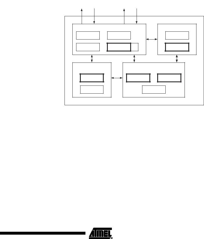
- •Features
- •Pin Configurations
- •Disclaimer
- •Overview
- •Block Diagram
- •Pin Descriptions
- •Port A (PA7..PA0)
- •Port B (PB7..PB0)
- •Port C (PC7..PC0)
- •Port D (PD7..PD0)
- •RESET
- •XTAL1
- •XTAL2
- •AVCC
- •AREF
- •AVR CPU Core
- •Introduction
- •Architectural Overview
- •Status Register
- •Stack Pointer
- •Interrupt Response Time
- •SRAM Data Memory
- •Data Memory Access Times
- •EEPROM Data Memory
- •EEPROM Read/Write Access
- •I/O Memory
- •Clock Systems and their Distribution
- •CPU Clock – clkCPU
- •I/O Clock – clkI/O
- •Flash Clock – clkFLASH
- •ADC Clock – clkADC
- •Clock Sources
- •Default Clock Source
- •Crystal Oscillator
- •External RC Oscillator
- •External Clock
- •Timer/Counter Oscillator
- •Idle Mode
- •Power-down Mode
- •Power-save Mode
- •Standby Mode
- •Extended Standby Mode
- •Analog to Digital Converter
- •Analog Comparator
- •Brown-out Detector
- •Internal Voltage Reference
- •Watchdog Timer
- •Port Pins
- •Resetting the AVR
- •Reset Sources
- •Power-on Reset
- •External Reset
- •Brown-out Detection
- •Watchdog Reset
- •Watchdog Timer
- •Interrupts
- •I/O Ports
- •Introduction
- •Configuring the Pin
- •Reading the Pin Value
- •Unconnected pins
- •Alternate Port Functions
- •Alternate Functions of Port A
- •Alternate Functions of Port B
- •Alternate Functions of Port C
- •Alternate Functions of Port D
- •Port A Data Register – PORTA
- •Port B Data Register – PORTB
- •Port C Data Register – PORTC
- •Port D Data Register – PORTD
- •External Interrupts
- •8-bit Timer/Counter0 with PWM
- •Overview
- •Registers
- •Definitions
- •Counter Unit
- •Output Compare Unit
- •Force Output Compare
- •Modes of Operation
- •Normal Mode
- •Fast PWM Mode
- •Phase Correct PWM Mode
- •Internal Clock Source
- •Prescaler Reset
- •External Clock Source
- •16-bit Timer/Counter1
- •Overview
- •Registers
- •Definitions
- •Compatibility
- •Counter Unit
- •Input Capture Unit
- •Input Capture Trigger Source
- •Noise Canceler
- •Using the Input Capture Unit
- •Output Compare Units
- •Force Output Compare
- •Modes of Operation
- •Normal Mode
- •Fast PWM Mode
- •Phase Correct PWM Mode
- •8-bit Timer/Counter2 with PWM and Asynchronous Operation
- •Overview
- •Registers
- •Definitions
- •Counter Unit
- •Output Compare Unit
- •Force Output Compare
- •Modes of Operation
- •Normal Mode
- •Fast PWM Mode
- •Phase Correct PWM Mode
- •Timer/Counter Prescaler
- •SS Pin Functionality
- •Slave Mode
- •Master Mode
- •SPI Control Register – SPCR
- •SPI Status Register – SPSR
- •SPI Data Register – SPDR
- •Data Modes
- •USART
- •Overview
- •AVR USART vs. AVR UART – Compatibility
- •Clock Generation
- •External Clock
- •Synchronous Clock Operation
- •Frame Formats
- •Parity Bit Calculation
- •USART Initialization
- •Parity Generator
- •Disabling the Transmitter
- •Receiver Error Flags
- •Parity Checker
- •Disabling the Receiver
- •Flushing the Receive Buffer
- •Asynchronous Data Recovery
- •Using MPCM
- •Write Access
- •Read Access
- •Two-wire Serial Interface
- •Features
- •TWI Terminology
- •Electrical Interconnection
- •Transferring Bits
- •START and STOP Conditions
- •Address Packet Format
- •Data Packet Format
- •Overview of the TWI Module
- •SCL and SDA Pins
- •Bit Rate Generator Unit
- •Bus Interface Unit
- •Address Match Unit
- •Control Unit
- •TWI Register Description
- •TWI Bit Rate Register – TWBR
- •TWI Control Register – TWCR
- •TWI Status Register – TWSR
- •TWI Data Register – TWDR
- •Using the TWI
- •Transmission Modes
- •Master Transmitter Mode
- •Master Receiver Mode
- •Slave Receiver Mode
- •Slave Transmitter Mode
- •Miscellaneous States
- •Analog Comparator
- •Analog Comparator Multiplexed Input
- •Features
- •Operation
- •Starting a Conversion
- •Differential Gain Channels
- •Changing Channel or Reference Selection
- •ADC Input Channels
- •ADC Voltage Reference
- •ADC Noise Canceler
- •Analog Input Circuitry
- •ADC Accuracy Definitions
- •ADC Conversion Result
- •ADLAR = 0
- •ADLAR = 1
- •Features
- •Overview
- •Test Access Port – TAP
- •TAP Controller
- •PRIVATE0; $8
- •PRIVATE1; $9
- •PRIVATE2; $A
- •PRIVATE3; $B
- •Bibliography
- •Features
- •System Overview
- •Data Registers
- •Bypass Register
- •Device Identification Register
- •Reset Register
- •Boundary-scan Chain
- •EXTEST; $0
- •IDCODE; $1
- •SAMPLE_PRELOAD; $2
- •AVR_RESET; $C
- •BYPASS; $F
- •Scanning the Digital Port Pins
- •Scanning the RESET Pin
- •Scanning the Clock Pins
- •Scanning the ADC
- •Features
- •Application Section
- •BLS – Boot Loader Section
- •Read-While-Write and no Read-While-Write Flash Sections
- •Boot Loader Lock Bits
- •Performing a Page Write
- •Using the SPM Interrupt
- •Setting the Boot Loader Lock Bits by SPM
- •Reading the Fuse and Lock Bits from Software
- •Preventing Flash Corruption
- •Fuse Bits
- •Latching of Fuses
- •Signature Bytes
- •Calibration Byte
- •Signal Names
- •Parallel Programming
- •Enter Programming Mode
- •Chip Erase
- •Programming the Flash
- •Programming the EEPROM
- •Reading the Flash
- •Reading the EEPROM
- •Programming the Lock Bits
- •Reading the Signature Bytes
- •Reading the Calibration Byte
- •SPI Serial Downloading
- •Data Polling Flash
- •Data Polling EEPROM
- •AVR_RESET ($C)
- •PROG_ENABLE ($4)
- •PROG_COMMANDS ($5)
- •PROG_PAGELOAD ($6)
- •PROG_PAGEREAD ($7)
- •Data Registers
- •Reset Register
- •Programming Enable Register
- •Virtual Flash Page Read Register
- •Programming Algorithm
- •Entering Programming Mode
- •Leaving Programming Mode
- •Performing Chip Erase
- •Programming the Flash
- •Reading the Flash
- •Programming the EEPROM
- •Reading the EEPROM
- •Programming the Fuses
- •Programming the Lock Bits
- •Reading the Signature Bytes
- •Reading the Calibration Byte
- •Electrical Characteristics
- •Absolute Maximum Ratings*
- •DC Characteristics
- •External Clock Drive Waveforms
- •External Clock Drive
- •Two-wire Serial Interface Characteristics
- •ADC Characteristics
- •Register Summary
- •Instruction Set Summary
- •Ordering Information
- •Packaging Information
- •Errata
- •ATmega32 Rev. A
- •Datasheet Change Log for ATmega32
- •Changes from Rev. 2503E-09/03 to Rev. 2503F-12/03
- •Changes from Rev. 2503D-02/03 to Rev. 2503E-09/03
- •Changes from Rev. 2503C-10/02 to Rev. 2503D-02/03
- •Changes from Rev. 2503B-10/02 to Rev. 2503C-10/02
- •Changes from Rev. 2503A-03/02 to Rev. 2503B-10/02
- •Table of Contents
ATmega32(L)
Overview of the TWI
Module
The TWI module is comprised of several submodules, as shown in Figure 84. All registers drawn in a thick line are accessible through the AVR data bus.
Figure 84. Overview of the TWI Module
SCL |
|
SDA |
||
|
|
|
|
|
Slew-rate |
Spike |
|
Slew-rate |
Spike |
Control |
Filter |
|
Control |
Filter |
|
|
|
|
|
Bus Interface Unit |
|
Bit Rate Generator |
||
START / STOP |
Spike Suppression |
|
Prescaler |
|
Control |
|
|||
|
|
|
||
Arbitration detection |
Address/Data Shift |
Ack |
Bit Rate Register |
|
Register (TWDR) |
(TWBR) |
|||
|
|
|||
Address Match Unit |
|
Control Unit |
||
Address Register |
|
Status Register |
Control Register |
|
(TWAR) |
|
(TWSR) |
(TWCR) |
|
|
|
|
TWI Unit |
|
Address Comparator |
|
State Machine and |
||
|
|
Status control |
||
|
|
|
SCL and SDA Pins |
These pins interface the AVR TWI with the rest of the MCU system. The output drivers |
|
contain a slew-rate limiter in order to conform to the TWI specification. The input stages |
|
contain a spike suppression unit removing spikes shorter than 50 ns. Note that the inter- |
|
nal pullups in the AVR pads can be enabled by setting the PORT bits corresponding to |
|
the SCL and SDA pins, as explained in the I/O Port section. The internal pull-ups can in |
|
some systems eliminate the need for external ones. |
Bit Rate Generator Unit |
This unit controls the period of SCL when operating in a Master mode. The SCL period |
|
is controlled by settings in the TWI Bit Rate Register (TWBR) and the Prescaler bits in |
|
the TWI Status Register (TWSR). Slave operation does not depend on Bit Rate or Pres- |
|
caler settings, but the CPU clock frequency in the slave must be at least 16 times higher |
|
than the SCL frequency. Note that slaves may prolong the SCL low period, thereby |
|
reducing the average TWI bus clock period. The SCL frequency is generated according |
|
to the following equation: |
|
SCL frequency = --CPU--------------Clock-----------------frequency------------------------- |
|
16 + 2(TWBR) 4TW PS |
•TWBR = Value of the TWI Bit Rate Register
•TWPS = Value of the prescaler bits in the TWI Status Register
Note: TWBR should be 10 or higher if the TWI operates in Master mode. If TWBR is lower than 10, the master may produce an incorrect output on SDA and SCL for the reminder of the byte. The problem occurs when operating the TWI in Master mode, sending Start + SLA + R/W to a slave (a slave does not need to be connected to the bus for the condition to happen).
173
2503F–AVR–12/03
Bus Interface Unit |
|
|
|
|
|
|
|
|
|
|
|
This unit contains the Data and Address Shift Register (TWDR), a START/STOP Con- |
|||||
|
troller and Arbitration detection hardware. The TWDR contains the address or data |
||||
|
bytes to be transmitted, or the address or data bytes received. In addition to the 8-bit |
||||
|
TWDR, the Bus Interface Unit also contains a register containing the (N)ACK bit to be |
||||
|
transmitted or received. This (N)ACK Register is not directly accessible by the applica- |
||||
|
tion software. However, when receiving, it can be set or cleared by manipulating the |
||||
|
TWI Control Register (TWCR). When in Transmitter mode, the value of the received |
||||
|
(N)ACK bit can be determined by the value in the TWSR. |
||||
|
The START/STOP Controller is responsible for generation and detection of START, |
||||
|
REPEATED START, and STOP conditions. The START/STOP controller is able to |
||||
|
detect START and STOP conditions even when the AVR MCU is in one of the sleep |
||||
|
modes, enabling the MCU to wake up if addressed by a master. |
||||
|
If the TWI has initiated a transmission as master, the Arbitration Detection hardware |
||||
|
continuously monitors the transmission trying to determine if arbitration is in process. If |
||||
|
the TWI has lost an arbitration, the Control Unit is informed. Correct action can then be |
||||
|
taken and appropriate status codes generated. |
||||
Address Match Unit |
The Address Match unit checks if received address bytes match the 7-bit address in the |
||||
|
TWI Address Register (TWAR). If the TWI General Call Recognition Enable (TWGCE) |
||||
|
bit in the TWAR is written to one, all incoming address bits will also be compared |
||||
|
against the General Call address. Upon an address match, the Control Unit is informed, |
||||
|
allowing correct action to be taken. The TWI may or may not acknowledge its address, |
||||
|
depending on settings in the TWCR. The Address Match unit is able to compare |
||||
|
addresses even when the AVR MCU is in sleep mode, enabling the MCU to wake up if |
||||
|
addressed by a master. |
||||
Control Unit |
The Control unit monitors the TWI bus and generates responses corresponding to set- |
||||
|
tings in the TWI Control Register (TWCR). When an event requiring the attention of the |
||||
|
application occurs on the TWI bus, the TWI Interrupt Flag (TWINT) is asserted. In the |
||||
|
next clock cycle, the TWI Status Register (TWSR) is updated with a status code identify- |
||||
|
ing the event. The TWSR only contains relevant status information when the TWI |
||||
|
Interrupt Flag is asserted. At all other times, the TWSR contains a special status code |
||||
|
indicating that no relevant status information is available. As long as the TWINT Flag is |
||||
|
set, the SCL line is held low. This allows the application software to complete its tasks |
||||
|
before allowing the TWI transmission to continue. |
The TWINT Flag is set in the following situations:
•After the TWI has transmitted a START/REPEATED START condition
•After the TWI has transmitted SLA+R/W
•After the TWI has transmitted an address byte
•After the TWI has lost arbitration
•After the TWI has been addressed by own slave address or general call
•After the TWI has received a data byte
•After a STOP or REPEATED START has been received while still addressed as a slave
•When a bus error has occurred due to an illegal START or STOP condition
174 ATmega32(L)
2503F–AVR–12/03