

USART Initialization |
|
|
|
|
|
|
|
|
|
|
|
|
|
The USART has to be initialized before any communication can take place. The initial- |
||||||
|
ization process normally consists of setting the baud rate, setting frame format and |
|||||
|
enabling the Transmitter or the Receiver depending on the usage. For interrupt driven |
|||||
|
USART operation, the Global Interrupt Flag should be cleared (and interrupts globally |
|||||
|
disabled) when doing the initialization. |
|||||
|
Before doing a re-initialization with changed baud rate or frame format, be sure that |
|||||
|
there are no ongoing transmissions during the period the registers are changed. The |
|||||
|
TXC Flag can be used to check that the Transmitter has completed all transfers, and the |
|||||
|
RXC Flag can be used to check that there are no unread data in the receive buffer. Note |
|||||
|
that the TXC Flag must be cleared before each transmission (before UDR is written) if it |
|||||
|
is used for this purpose. |
|||||
|
The following simple USART initialization code examples show one assembly and one |
|||||
|
C function that are equal in functionality. The examples assume asynchronous opera- |
|||||
|
tion using polling (no interrupts enabled) and a fixed frame format. The baud rate is |
|||||
|
given as a function parameter. For the assembly code, the baud rate parameter is |
|||||
|
assumed to be stored in the r17:r16 registers. When the function writes to the UCSRC |
|||||
|
Register, the URSEL bit (MSB) must be set due to the sharing of I/O location by UBRRH |
|||||
|
and UCSRC. |
|||||
|
|
|||||
|
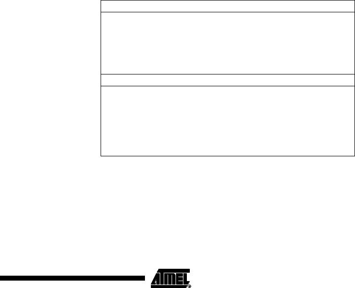
Assembly Code Example(1) |
|||||
|
|
|||||
|
USART_Init: |
|||||
|
; Set baud rate |
|||||
|
out |
UBRRH, r17 |
||||
|
out |
UBRRL, r16 |
||||
|
; Enable receiver and transmitter |
|||||
|
ldi |
r16, (1<<RXEN)|(1<<TXEN) |
||||
|
out |
UCSRB,r16 |
||||
|
; Set frame format: 8data, 2stop bit |
|||||
|
ldi |
r16, (1<<URSEL)|(1<<USBS)|(3<<UCSZ0) |
||||
|
out |
UCSRC,r16 |
||||
|
ret |
|
|
|
|
|
|
|
|||||
|
C Code Example(1) |
|||||
|
|
|||||
|
void USART_Init( unsigned int baud ) |
|||||
|
{ |
|
|
|
|
|
|
/* Set baud rate */ |
|||||
|
UBRRH = (unsigned char)(baud>>8); |
|||||
|
UBRRL = (unsigned char)baud; |
|||||
|
/* Enable receiver and transmitter */ |
|||||
|
UCSRB = (1<<RXEN)|(1<<TXEN); |
|||||
|
/* Set frame format: 8data, 2stop bit */ |
|||||
|
UCSRC = (1<<URSEL)|(1<<USBS)|(3<<UCSZ0); |
|||||
|
} |
|
|
|
|
|
|
|
|
||||
|
Note: 1. |
The example code assumes that the part specific header file is included. |
||||
|
More advanced initialization routines can be made that include frame format as parame- |
|||||
ters, disable interrupts and so on. However, many applications use a fixed setting of the Baud and Control Registers, and for these types of applications the initialization code can be placed directly in the main routine, or be combined with initialization code for other I/O modules.
144 ATmega32(L)
2503F–AVR–12/03
 ATmega32(L)
Data Transmission – The
USART Transmitter
The USART Transmitter is enabled by setting the Transmit Enable (TXEN) bit in the UCSRB Register. When the Transmitter is enabled, the normal port operation of the TxD pin is overridden by the USART and given the function as the transmitter’s serial output. The baud rate, mode of operation and frame format must be set up once before doing any transmissions. If synchronous operation is used, the clock on the XCK pin will be overridden and used as transmission clock.
Sending Frames with 5 to 8 A data transmission is initiated by loading the transmit buffer with the data to be trans- Data Bit mitted. The CPU can load the transmit buffer by writing to the UDR I/O location. The buffered data in the transmit buffer will be moved to the Shift Register when the Shift Register is ready to send a new frame. The Shift Register is loaded with new data if it is in idle state (no ongoing transmission) or immediately after the last stop bit of the previous frame is transmitted. When the Shift Register is loaded with new data, it will transfer one complete frame at the rate given by the Baud Register, U2X bit or by XCK depend-
ing on mode of operation.
The following code examples show a simple USART transmit function based on polling of the Data Register Empty (UDRE) Flag. When using frames with less than eight bits, the most significant bits written to the UDR are ignored. The USART has to be initialized before the function can be used. For the assembly code, the data to be sent is assumed to be stored in Register R16
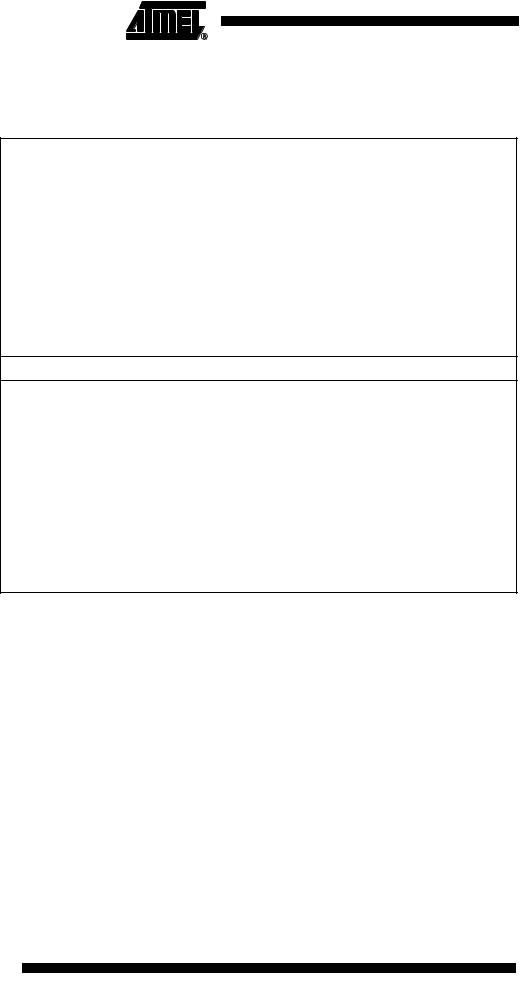
Assembly Code Example(1)
USART_Transmit:
; Wait for empty transmit buffer sbis UCSRA,UDRE
rjmp USART_Transmit
; Put data (r16) into buffer, sends the data out UDR,r16
ret
C Code Example(1)
void USART_Transmit( unsigned char data )
{
/* Wait for empty transmit buffer */ while ( !( UCSRA & (1<<UDRE)) )
;
/* Put data into buffer, sends the data */ UDR = data;
}
Note: 1. The example code assumes that the part specific header file is included.
The function simply waits for the transmit buffer to be empty by checking the UDRE Flag, before loading it with new data to be transmitted. If the Data Register Empty Interrupt is utilized, the interrupt routine writes the data into the buffer.
145
2503F–AVR–12/03
Sending Frames with 9 Data Bit
If 9-bit characters are used (UCSZ = 7), the ninth bit must be written to the TXB8 bit in UCSRB before the low byte of the character is written to UDR. The following code examples show a transmit function that handles 9-bit characters. For the assembly code, the data to be sent is assumed to be stored in Registers R17:R16.
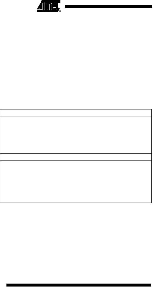
Assembly Code Example(1)
USART_Transmit:
; Wait for empty transmit buffer
sbis UCSRA,UDRE rjmp USART_Transmit
; Copy 9th bit from r17 to TXB8 cbi UCSRB,TXB8
sbrc r17,0
sbi UCSRB,TXB8
; Put LSB data (r16) into buffer, sends the data out UDR,r16
ret
C Code Example(1)
void USART_Transmit( unsigned int data )
{
/* Wait for empty transmit buffer */ while ( !( UCSRA & (1<<UDRE))) )
;
/* Copy 9th bit to TXB8 */ UCSRB &= ~(1<<TXB8);
if ( data & 0x0100 ) UCSRB |= (1<<TXB8);
/* Put data into buffer, sends the data */ UDR = data;
}
|
Note: 1. These transmit functions are written to be general functions. They can be optimized if |
|
the contents of the UCSRB is static. (i.e., only the TXB8 bit of the UCSRB Register is |
|
used after initialization). |
|
The ninth bit can be used for indicating an address frame when using multi processor |
|
communication mode or for other protocol handling as for example synchronization. |
Transmitter Flags and |
The USART transmitter has two flags that indicate its state: USART Data Register |
Interrupts |
Empty (UDRE) and Transmit Complete (TXC). Both flags can be used for generating |
|
interrupts. |
|
The Data Register Empty (UDRE) Flag indicates whether the transmit buffer is ready to |
|
receive new data. This bit is set when the transmit buffer is empty, and cleared when the |
|
transmit buffer contains data to be transmitted that has not yet been moved into the Shift |
|
Register. For compatibility with future devices, always write this bit to zero when writing |
|
the UCSRA Register. |
|
When the Data Register empty Interrupt Enable (UDRIE) bit in UCSRB is written to one, |
|
the USART Data Register Empty Interrupt will be executed as long as UDRE is set (pro- |
|
vided that global interrupts are enabled). UDRE is cleared by writing UDR. When |
|
interrupt-driven data transmission is used, the Data Register Empty Interrupt routine |
|
must either write new data to UDR in order to clear UDRE or disable the Data Register |
146 ATmega32(L)
2503F–AVR–12/03

 ATmega32(L)
empty Interrupt, otherwise a new interrupt will occur once the interrupt routine
|
terminates. |
|
The Transmit Complete (TXC) Flag bit is set one when the entire frame in the transmit |
|
Shift Register has been shifted out and there are no new data currently present in the |
|
transmit buffer. The TXC Flag bit is automatically cleared when a transmit complete |
|
interrupt is executed, or it can be cleared by writing a one to its bit location. The TXC |
|
Flag is useful in half-duplex communication interfaces (like the RS485 standard), where |
|
a transmitting application must enter receive mode and free the communication bus |
|
immediately after completing the transmission. |
|
When the Transmit Compete Interrupt Enable (TXCIE) bit in UCSRB is set, the USART |
|
Transmit Complete Interrupt will be executed when the TXC Flag becomes set (pro- |
|
vided that global interrupts are enabled). When the transmit complete interrupt is used, |
|
the interrupt handling routine does not have to clear the TXC Flag, this is done automat- |
|
ically when the interrupt is executed. |
Parity Generator |
The parity generator calculates the parity bit for the serial frame data. When parity bit is |
|
enabled (UPM1 = 1), the transmitter control logic inserts the parity bit between the last |
|
data bit and the first stop bit of the frame that is sent. |
Disabling the Transmitter |
The disabling of the transmitter (setting the TXEN to zero) will not become effective until |
|
ongoing and pending transmissions are completed, i.e., when the transmit Shift Register |
|
and transmit Buffer Register do not contain data to be transmitted. When disabled, the |
|
transmitter will no longer override the TxD pin. |
147
2503F–AVR–12/03
Data Reception – The
USART Receiver
The USART Receiver is enabled by writing the Receive Enable (RXEN) bit in the UCSRB Register to one. When the receiver is enabled, the normal pin operation of the RxD pin is overridden by the USART and given the function as the receiver’s serial input. The baud rate, mode of operation and frame format must be set up once before any serial reception can be done. If synchronous operation is used, the clock on the XCK pin will be used as transfer clock.
Receiving Frames with 5 to 8 The receiver starts data reception when it detects a valid start bit. Each bit that follows Data Bits the start bit will be sampled at the baud rate or XCK clock, and shifted into the receive Shift Register until the first stop bit of a frame is received. A second stop bit will be ignored by the receiver. When the first stop bit is received, i.e., a complete serial frame is present in the receive Shift Register, the contents of the Shift Register will be moved into the receive buffer. The receive buffer can then be read by reading the UDR I/O
location.
The following code example shows a simple USART receive function based on polling of the Receive Complete (RXC) Flag. When using frames with less than eight bits the most significant bits of the data read from the UDR will be masked to zero. The USART has to be initialized before the function can be used.
Assembly Code Example(1)
USART_Receive:
; Wait for data to be received sbis UCSRA, RXC
rjmp USART_Receive
; Get and return received data from buffer in r16, UDR
ret
C Code Example(1)
unsigned char USART_Receive( void )
{
/* Wait for data to be received */ while ( !(UCSRA & (1<<RXC)) )
;
/* Get and return received data from buffer */ return UDR;
}
Note: 1. The example code assumes that the part specific header file is included.
The function simply waits for data to be present in the receive buffer by checking the
RXC Flag, before reading the buffer and returning the value.
148 ATmega32(L)
2503F–AVR–12/03
ATmega32(L)
Receiving Frames with 9 If 9 bit characters are used (UCSZ=7) the ninth bit must be read from the RXB8 bit in Databits UCSRB before reading the low bits from the UDR. This rule applies to the FE, DOR and PE Status Flags as well. Read status from UCSRA, then data from UDR. Reading the UDR I/O location will change the state of the receive buffer FIFO and consequently the
TXB8, FE, DOR and PE bits, which all are stored in the FIFO, will change.
The following code example shows a simple USART receive function that handles both 9-bit characters and the status bits.
Assembly Code Example(1) |
||
|
|
|
|
USART_Receive: |
|
|
; Wait for data to be received |
|
|
sbis |
UCSRA, RXC |
|
rjmp |
USART_Receive |
|
; Get status and 9th bit, then data from buffer |
|
|
in |
r18, UCSRA |
|
in |
r17, UCSRB |
|
in |
r16, UDR |
|
; If error, return -1 |
|
|
andi |
r18,(1<<FE)|(1<<DOR)|(1<<PE) |
|
breq |
USART_ReceiveNoError |
|
ldi |
r17, HIGH(-1) |
|
ldi |
r16, LOW(-1) |
|
USART_ReceiveNoError: |
|
|
; Filter the 9th bit, then return |
|
|
lsr |
r17 |
|
andi |
r17, 0x01 |
|
ret |
|
|
||
C Code Example(1) |
||
|
|
|
|
unsigned int USART_Receive( void ) |
|
|
{ |
|
|
unsigned char status, resh, resl; |
|
|
/* Wait for data to be received */ |
|
|
while ( !(UCSRA & (1<<RXC)) ) |
|
|
|
; |
|
/* Get status and 9th bit, then data */ |
|
|
/* from buffer */ |
|
|
status = UCSRA; |
|
|
resh = UCSRB; |
|
|
resl = UDR; |
|
|
/* If error, return -1 */ |
|
|
if ( status & (1<<FE)|(1<<DOR)|(1<<PE) ) |
|
|
return -1; |
|
|
/* Filter the 9th bit, then return */ |
|
|
resh = (resh >> 1) & 0x01; |
|
|
return ((resh << 8) | resl); |
|
|
} |
|
|
|
|
Note: |
1. The example code assumes that the part specific header file is included. |
|
149
2503F–AVR–12/03