ATmega32(L)
Boundary-scan Chain The Boundary-scan chain has the capability of driving and observing the logic levels on the digital I/O pins, as well as the boundary between digital and analog logic for analog circuitry having Off-chip connection.
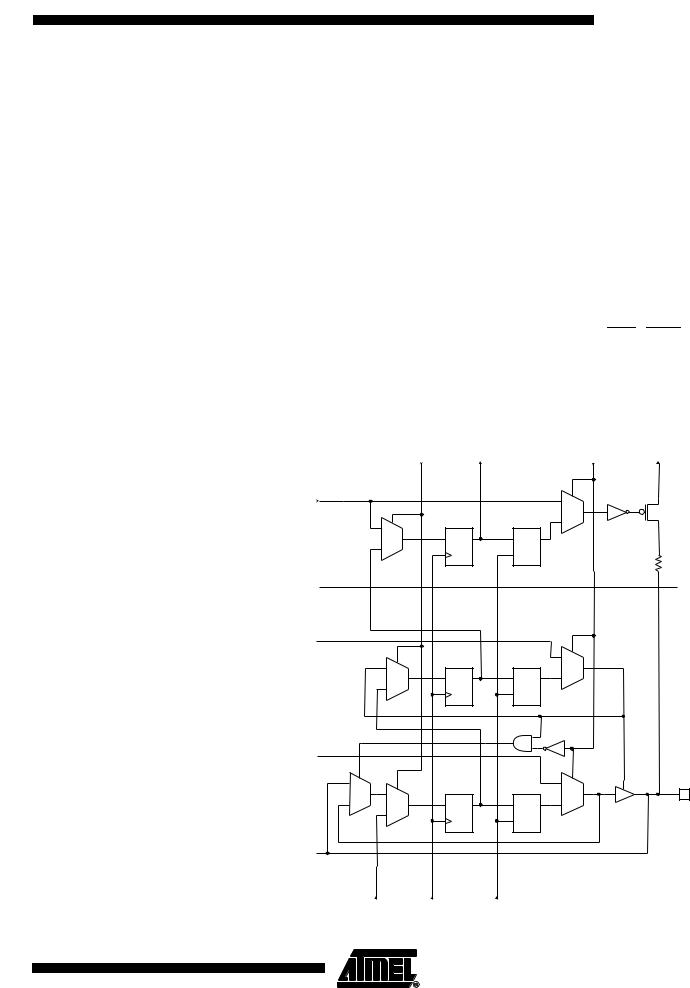
Scanning the Digital Port Pins Figure 116 shows the Boundary-scan Cell for a bi-directional port pin with pull-up function. The cell consists of a standard Boundary-scan cell for the Pull-up Enable – PUExn
– function, and a bi-directional pin cell that combines the three signals Output Control – OCxn, Output Data – ODxn, and Input Data – IDxn, into only a two-stage Shift Register. The port and pin indexes are not used in the following description.
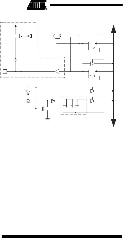
The Boundary-scan logic is not included in the figures in the datasheet. Figure 117 shows a simple digital Port Pin as described in the section “I/O Ports” on page 47. The Boundary-scan details from Figure 116 replaces the dashed box in Figure 117.
When no alternate port function is present, the Input Data – ID – corresponds to the PINxn Register value (but ID has no synchronizer), Output Data corresponds to the PORT Register, Output Control corresponds to the Data Direction – DD Register, and the Pull-up Enable – PUExn – corresponds to logic expression PUD · DDxn · PORTxn.
Digital alternate port functions are connected outside the dotted box in Figure 117 to make the scan chain read the actual pin value. For Analog function, there is a direct connection from the external pin to the analog circuit, and a scan chain is inserted on the interface between the digital logic and the analog circuitry.
Figure 116. Boundary-scan Cell for Bidirectional Port Pin with Pull-up Function.
ShiftDR |
To Next Cell |
|
EXTEST |
Vcc |
Pullup Enable (PUE) |
|
|
0 |
|
|
|
|
|
FF2 |
LD2 |
1 |
|
0 |
|
|
|
|
|
|
|
D |
Q |
D Q |
|
|
1 |
|
G |
|
|
|
|
|
|
Output Control (OC) 
|
FF1 |
LD1 |
0 |
|
0 |
|
1 |
|
D Q |
D Q |
|
|
|
1 |
G |
|
|
|
|
Output Data (OD) 
|
0 |
FF0 |
LD0 |
0 |
|
|
0 |
|
Port Pin (PXn) |
|
1 |
|
1 |
|
D Q |
D Q |
|
|
|
|
|
1 |
G |
|
|
|
|
|
Input Data (ID)
From Last Cell |
ClockDR |
UpdateDR |
227
2503F–AVR–12/03
Figure 117. General Port Pin Schematic Diagram(1)
Boundary-scan and the Twowire Interface
PUExn |
|
|
|
|
PUD |
|
|
|
|
|
|
|
|
|
|
Q |
D |
|
|
|
|
|
DDxn |
|
|
|
|
|
Q CLR |
|
|
|
|
|
|
RESET |
WDx |
|
OCxn |
|
|
|
|
|
|
|
|
|
|
|
|
|
|
|
RDx |
|
Pxn |
|
|
Q |
D |
|
BUS |
|
|
|
DATA |
ODxn |
|
PORTxn |
|
|
|
|
|
|
|
Q CLR |
|
|
|
IDxn |
|
|
RESET |
WPx |
|
|
|
|
|
|
SLEEP |
|
|
|
|
RRx |
|
SYNCHRONIZER |
|
RPx |
|
|
|
|
|
|
|
D |
Q |
D |
Q |
|
|
|
|
|
PINxn |
|
|
|
L |
Q |
|
Q |
|
|
|
|
|
|
|
|
CLK I/O |
|
|
PUD: |
PULLUP DISABLE |
WDx: |
WRITE DDRx |
|
PUExn: |
PULLUP ENABLE for pin Pxn |
RDx: |
READ DDRx |
|
OCxn: |
OUTPUT CONTROL for pin Pxn |
WPx: |
WRITE PORTx |
|
ODxn: |
OUTPUT DATA to pin Pxn |
RRx: |
READ PORTx REGISTER |
|
IDxn: |
INPUT DATA from pin Pxn |
RPx: |
READ PORTx PIN |
|
SLEEP: |
SLEEP CONTROL |
CLK I/O : |
I/O CLOCK |
Note: |
1. See Boundary-scan descriptin for details. |
|
|
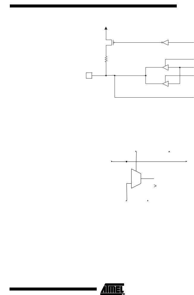
The 2 Two-wire Interface pins SCL and SDA have one additional control signal in the scan-chain; Two-wire Interface Enable – TWIEN. As shown in Figure 118, the TWIEN signal enables a tri-state buffer with slew-rate control in parallel with the ordinary digital port pins. A general scan cell as shown in Figure 122 is attached to the TWIEN signal.
Notes: 1. A separate scan chain for the 50 ns spike filter on the input is not provided. The ordinary scan support for digital port pins suffice for connectivity tests. The only reason for having TWIEN in the scan path, is to be able to disconnect the slew-rate control buffer when doing boundary-scan.
2.Make sure the OC and TWIEN signals are not asserted simultaneously, as this will lead to drive contention.
ATmega32(L)
Figure 118. Additional Scan Signal for the Two-wire Interface
PUExn
|
|
|
|
|
|
Slew-rate Limited |
|
|
|
|
|
|
|
|
|
IDxn |
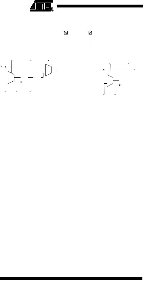
Scanning the RESET Pin |
The RESET pin accepts 5V active low logic for standard reset operation, and 12V active |
|
high logic for High Voltage Parallel Programming. An observe-only cell as shown in Fig- |
|
ure 119 is inserted both for the 5V reset signal; RSTT, and the 12V reset signal; |
|
RSTHV. |
|
|
|
|
Figure 119. Observe-only Cell |
|
|
|
|
|
|
|
|
|
|
|
To |
|
|
|
|
|
|
|
Next |
|
|
|
ShiftDR |
Cell |
|
From System Pin |
|
|
|
|
|
|
To System Logic |
|
|
|
|
|
|
|
|
|
|
|
|
|
|
|
|
FF1 |
|
|
|
|
|
0 |
|
|
|
|
|
|
|
|
|
D |
Q |
|
|
|
1 |
|
|
|
|
|
|
|
|
|
|
|
|
|
|
|
|
|
|
|
|
|
|
|
|
|
|
|
|
|
|
|
|
|
|
|
|
|
|
|
|
|
|
|
From ClockDR
Previous
Cell
Scanning the Clock Pins The AVR devices have many clock options selectable by fuses. These are: Internal RC Oscillator, External RC, External Clock, (High Frequency) Crystal Oscillator, Low Frequency Crystal Oscillator, and Ceramic Resonator.
Figure 120 shows how each Oscillator with external connection is supported in the scan chain. The Enable signal is supported with a general boundary-scan cell, while the Oscillator/Clock output is attached to an observe-only cell. In addition to the main clock, the Timer Oscillator is scanned in the same way. The output from the internal RC Oscillator is not scanned, as this Oscillator does not have external connections.
229
2503F–AVR–12/03
Figure 120. Boundary-scan Cells for Oscillators and Clock Options
XTAL1/TOSC1 XTAL2/TOSC2
|
|
|
|
|
|
|
To |
|
|
|
|
|
|
|
|
|
|
|
|
|
|
|
|
|
|
|
|
|
|
|
|
|
|
|
|
|
|
|
|
|
|
|
|
|
|
|
|
|
|
|
|
|
|
|
|
|
|
|
|
|
|
|
|
|
|
|
|
|
|
|
|
|
|
|
|
|
|
|
Next |
|
|
|
|
|
|
Oscillator |
|
|
|
|
|
|
|
|
To |
|
ShiftDR |
|
Cell |
|
EXTEST |
|
|
|
|
|
|
|
|
|
|
Next |
|
|
|
|
|
|
|
|
|
|
0 |
|
ENABLE |
OUTPUT |
|
ShiftDR |
Cell |
|
|
|
|
|
|
|
|
|
|
|
|
|
|
|
|
|
|
|
|
|
|
|
|
|
|
|
|
|
|
|
|
|
|
|
|
|
|
|
|
|
|
|
|
|
|
|
|
|
|
|
|
|
|
|
|
|
|
|
|
|
|
|
|
|
|
|
|
|
|
|
|
|
|
|
|
|
|
|
|
|
|
|
|
|
|
|
|
|
|
0 |
|
|
|
|
|
|
|
1 |
|
|
|
|
|
|
|
|
|
|
|
|
|
|
|
|
|
|
|
|
|
|
|
|
|
|
|
|
FF1 |
|
|
|
|
D |
Q |
|
|
|
D |
Q |
|
|
|
|
|
|
|
|
|
|
|
|
|
|
|
|
|
|
|
|
|
|
|
|
|
|
|
|
|
|
|
|
|
|
|
|
|
|
1 |
|
|
|
|
|
|
|
|
|
|
|
|
|
|
|
|
0 |
|
D |
Q |
|
|
|
|
|
|
|
|
|
|
G |
|
|
|
|
|
|
|
|
|
1 |
|
|
|
|
|
|
|
|
|
|
|
|
|
|
|
|
|
|
|
|
|
|
|
|
|
|
|
|
|
|
|
|
|
|
|
|
|
|
|
|
|
|
|
|
|
|
|
|
|
|
|
|
|
|
|
From ClockDR |
UpdateDR |
|
|
|
|
|
|
|
|
|
|
|
|
|
|
|
|
|
|
|
|
|
|
|
|
|
|
From ClockDR |
|
|
|
Previous |
|
|
|
|
|
|
|
|
|
|
|
|
|
|
|
|
|
Cell |
|
|
|
|
|
|
|
|
|
|
|
|
|
|
Previous |
|
|
|
|
|
|
|
|
|
|
|
|
|
|
|
|
|
|
|
|
|
|
Cell |
|
|
|
Table 90 summaries the scan registers for the external clock pin XTAL1, Oscillators with
XTAL1/XTAL2 connections as well as 32 kHz Timer Oscillator.
Table 90. Scan Signals for the Oscillators(1)(2)(3)
|
|
|
Scanned Clock Line |
Enable Signal |
Scanned Clock Line |
Clock Option |
when not Used |
|
|
|
|
EXTCLKEN |
EXTCLK (XTAL1) |
External Clock |
0 |
|
|
|
|
OSCON |
OSCCK |
External Crystal |
0 |
|
|
External Ceramic |
|
|
|
Resonator |
|
|
|
|
|
RCOSCEN |
RCCK |
External RC |
1 |
|
|
|
|
OSC32EN |
OSC32CK |
Low Freq. External Crystal |
0 |
|
|
|
|
TOSKON |
TOSCK |
32 kHz Timer Oscillator |
0 |
|
|
|
|
Notes: 1. Do not enable more than one clock source as main clock at a time.
2. Scanning an Oscillator output gives unpredictable results as there is a frequency drift between the Internal Oscillator and the JTAG TCK clock. If possible, scanning an external clock is preferred.
|
3. The clock configuration is programmed by fuses. As a fuse is not changed run-time, |
|
the clock configuration is considered fixed for a given application. The user is advised |
|
to scan the same clock option as to be used in the final system. The enable signals |
|
are supported in the scan chain because the system logic can disable clock options |
|
in sleep modes, thereby disconnecting the Oscillator pins from the scan path if not |
|
provided. The INTCAP fuses are not supported in the scan-chain, so the boundary |
|
scan chain can not make a XTAL Oscillator requiring internal capacitors to run unless |
|
the fuse is correctly programmed. |
Scanning the Analog |
The relevant Comparator signals regarding Boundary-scan are shown in Figure 121. |
Comparator |
The Boundary-scan cell from Figure 122 is attached to each of these signals. The sig- |
|
nals are described in Table 91. |
|
The Comparator need not be used for pure connectivity testing, since all analog inputs |
|
are shared with a digital port pin as well. |
230 ATmega32(L)
ATmega32(L)
Figure 121. Analog Comparator
BANDGAP
REFERENCE
ACBG
ACO
AC_IDLE
ACME
ADCEN 
ADC MULTIPLEXER
OUTPUT
Figure 122. General Boundary-scan Cell used for Signals for Comparator and ADC
|
|
|
|
|
|
|
To |
|
|
|
|
|
|
|
|
|
|
|
Next |
|
|
|
|
|
|
|
ShiftDR |
Cell |
|
EXTEST |
|
From Digital Logic/ |
|
|
|
|
|
|
|
0 |
|
|
|
|
|
|
|
|
|
|
|
|
|
|
|
|
|
|
|
|
|
|
|
|
|
|
|
|
|
|
From Analog Ciruitry |
|
|
|
|
|
|
|
|
|
|
To Analog Circuitry/ |
|
|
|
|
|
|
|
|
|
|
|
|
|
|
|
0 |
|
|
|
|
|
1 |
|
|
To Digital Logic |
|
|
|
|
D |
Q |
|
|
D Q |
|
|
|
|
1 |
|
|
|
|
|
|
|
|
|
|
|
|
|
|
|
|
|
|
|
G |
|
|
|
|
|
|
|
|
|
|
|
|
|
|
|
|
|
|
|
|
|
|
|
|
|
|
|
|
|
|
|
|
|
|
|
|
|
|
|
|
|
|
|
|
|
|
|
|
|
|
|
|
|
|
|
|
|
|
From ClockDR UpdateDR
Previous
Cell
231
2503F–AVR–12/03