

|
|
|
ATmega32(L) |
|
|
|
|
|
External Clock |
|
|
|
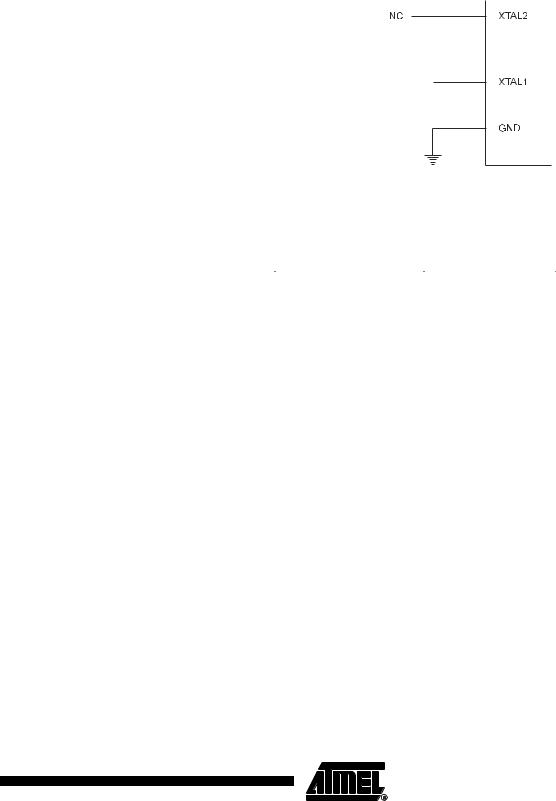
To drive the device from an external clock source, XTAL1 should be driven as shown in |
||
|
|||
|
|
Figure 14. To run the device on an external clock, the CKSEL fuses must be pro- |
|
|
|
grammed to “0000”. By programming the CKOPT Fuse, the user can enable an internal |
|
|
|
36 pF capacitor between XTAL1 and GND. |
|
|
|
Figure 14. External Clock Drive Configuration |
|
EXTERNAL
CLOCK
SIGNAL
When this clock source is selected, start-up times are determined by the SUT fuses as shown in Table 12.
Table 12. Start-up Times for the External Clock Selection
|
Start-up Time from |
Additional Delay |
|
|
Power-down and |
from Reset |
|
SUT1..0 |
Power-save |
(VCC = 5.0V) |
Recommended Usage |
00 |
6 CK |
– |
BOD enabled |
|
|
|
|
01 |
6 CK |
4.1 ms |
Fast rising power |
|
|
|
|
10 |
6 CK |
65 ms |
Slowly rising power |
|
|
|
|
11 |
|
Reserved |
|
|
|
|
|
When applying an external clock, it is required to avoid sudden changes in the applied clock frequency to ensure stable operation of the MCU. A variation in frequency of more than 2% from one clock cycle to the next can lead to unpredictable behavior. It is required to ensure that the MCU is kept in reset during such changes in the clock frequency.
Timer/Counter Oscillator For AVR microcontrollers with Timer/Counter Oscillator pins (TOSC1 and TOSC2), the crystal is connected directly between the pins. No external capacitors are needed. The Oscillator is optimized for use with a 32.768 kHz watch crystal. Applying an external clock source to TOSC1 is not recommended.
29
2503F–AVR–12/03

Power Management
and Sleep Modes
MCU Control Register –
MCUCR
Sleep modes enable the application to shut down unused modules in the MCU, thereby saving power. The AVR provides various sleep modes allowing the user to tailor the power consumption to the application’s requirements.
To enter any of the six sleep modes, the SE bit in MCUCR must be written to logic one and a SLEEP instruction must be executed. The SM2, SM1, and SM0 bits in the MCUCR Register select which sleep mode (Idle, ADC Noise Reduction, Power-down, Power-save, Standby, or Extended Standby) will be activated by the SLEEP instruction. See Table 13 for a summary. If an enabled interrupt occurs while the MCU is in a sleep mode, the MCU wakes up. The MCU is then halted for four cycles in addition to the start-up time, it executes the interrupt routine, and resumes execution from the instruction following SLEEP. The contents of the Register File and SRAM are unaltered when the device wakes up from sleep. If a Reset occurs during sleep mode, the MCU wakes up and executes from the Reset Vector.
Figure 11 on page 22 presents the different clock systems in the ATmega32, and their distribution. The figure is helpful in selecting an appropriate sleep mode.
The MCU Control Register contains control bits for power management.
Bit |
7 |
6 |
5 |
4 |
3 |
2 |
1 |
0 |
|
|
SE |
SM2 |
SM1 |
SM0 |
ISC11 |
ISC10 |
ISC01 |
ISC00 |
MCUCR |
Read/Write |
R/W |
R/W |
R/W |
R/W |
R/W |
R/W |
R/W |
R/W |
|
Initial Value |
0 |
0 |
0 |
0 |
0 |
0 |
0 |
0 |
|
• Bit 7 – SE: Sleep Enable
The SE bit must be written to logic one to make the MCU enter the sleep mode when the SLEEP instruction is executed. To avoid the MCU entering the sleep mode unless it is the programmers purpose, it is recommended to write the Sleep Enable (SE) bit to one just before the execution of the SLEEP instruction and to clear it immediately after waking up.
• Bits 6...4 – SM2..0: Sleep Mode Select Bits 2, 1, and 0
These bits select between the six available sleep modes as shown in Table 13.
Table 13. Sleep Mode Select
SM2 |
SM1 |
SM0 |
Sleep Mode |
|
|
|
|
0 |
0 |
0 |
Idle |
|
|
|
|
0 |
0 |
1 |
ADC Noise Reduction |
|
|
|
|
0 |
1 |
0 |
Power-down |
|
|
|
|
0 |
1 |
1 |
Power-save |
|
|
|
|
1 |
0 |
0 |
Reserved |
|
|
|
|
1 |
0 |
1 |
Reserved |
|
|
|
|
1 |
1 |
0 |
Standby(1) |
1 |
1 |
1 |
Extended Standby(1) |
Note: 1. Standby mode and Extended Standby mode are only available with external crystals or resonators.
30 ATmega32(L)
2503F–AVR–12/03
|
|
|
|
|
|
|
ATmega32(L) |
|
|
|
|
|
|
|
|
|
Idle Mode |
|
|
|
|
|
|
|
When the SM2..0 bits are written to 000, the SLEEP instruction makes the MCU enter |
||||||
|
|||||||
|
|
Idle mode, stopping the CPU but allowing SPI, USART, Analog Comparator, ADC, Two- |
|||||
|
|
wire Serial Interface, Timer/Counters, Watchdog, and the interrupt system to continue |
|||||
|
|
operating. This sleep mode basically halts clkCPU and clkFLASH, while allowing the other |
|||||
|
|
clocks to run. |
|||||
|
|
Idle mode enables the MCU to wake up from external triggered interrupts as well as |
|||||
|
|
internal ones like the Timer Overflow and USART Transmit Complete interrupts. If |
|||||
|
|
wake-up from the Analog Comparator interrupt is not required, the Analog Comparator |
|||||
|
|
can be powered down by setting the ACD bit in the Analog Comparator Control and Sta- |
|||||
|
|
tus Register – ACSR. This will reduce power consumption in Idle mode. If the ADC is |
|||||
|
|
enabled, a conversion starts automatically when this mode is entered. |
|||||
|
ADC Noise Reduction |
When the SM2..0 bits are written to 001, the SLEEP instruction makes the MCU enter |
|||||
|
Mode |
ADC Noise Reduction mode, stopping the CPU but allowing the ADC, the External Inter- |
|||||
|
|
rupts, the Two-wire Serial Interface address watch, Timer/Counter2 and the Watchdog |
|||||
|
|
to continue operating (if enabled). This sleep mode basically halts clkI/O, clkCPU, and clk- |
|||||
|
|
FLASH, while allowing the other clocks to run. |
|||||
|
|
This improves the noise environment for the ADC, enabling higher resolution measure- |
|||||
|
|
ments. If the ADC is enabled, a conversion starts automatically when this mode is |
|||||
|
|
entered. Apart form the ADC Conversion Complete interrupt, only an External Reset, a |
|||||
|
|
Watchdog Reset, a Brown-out Reset, a Two-wire Serial Interface Address Match Inter- |
|||||
|
|
rupt, a Timer/Counter2 interrupt, an SPM/EEPROM ready interrupt, an External level |
|||||
|
|
interrupt on INT0 or INT1, or an external interrupt on INT2 can wake up the MCU from |
|||||
|
|
ADC Noise Reduction mode. |
|||||
|
Power-down Mode |
When the SM2..0 bits are written to 010, the SLEEP instruction makes the MCU enter |
|||||
|
|
Power-down mode. In this mode, the External Oscillator is stopped, while the External |
|||||
|
|
interrupts, the Two-wire Serial Interface address watch, and the Watchdog continue |
|||||
|
|
operating (if enabled). Only an External Reset, a Watchdog Reset, a Brown-out Reset, a |
|||||
|
|
Two-wire Serial Interface address match interrupt, an External level interrupt on INT0 or |
|||||
|
|
INT1, or an External interrupt on INT2 can wake up the MCU. This sleep mode basically |
|||||
|
|
halts all generated clocks, allowing operation of asynchronous modules only. |
|||||
|
|
Note that if a level triggered interrupt is used for wake-up from Power-down mode, the |
|||||
|
|
changed level must be held for some time to wake up the MCU. Refer to “External Inter- |
|||||
|
|
rupts” on page 64 for details. |
|||||
|
|
When waking up from Power-down mode, there is a delay from the wake-up condition |
|||||
|
|
occurs until the wake-up becomes effective. This allows the clock to restart and become |
|||||
|
|
stable after having been stopped. The wake-up period is defined by the same CKSEL |
|||||
|
|
fuses that define the reset time-out period, as described in “Clock Sources” on page 23. |
|||||
|
Power-save Mode |
When the SM2..0 bits are written to 011, the SLEEP instruction makes the MCU enter |
|||||
|
|
Power-save mode. This mode is identical to Power-down, with one exception: |
|||||
|
|
If Timer/Counter2 is clocked asynchronously, i.e., the AS2 bit in ASSR is set, |
|||||
|
|
Timer/Counter2 will run during sleep. The device can wake up from either Timer Over- |
|||||
|
|
flow or Output Compare event from Timer/Counter2 if the corresponding |
|||||
|
|
Timer/Counter2 interrupt enable bits are set in TIMSK, and the Global Interrupt Enable |
|||||
|
|
bit in SREG is set. |
|||||
|
|
If the Asynchronous Timer is NOT clocked asynchronously, Power-down mode is rec- |
|||||
|
|
ommended instead of Power-save mode because the contents of the registers in the |
|||||
|
|
|
|
|
|
|
|
|
|
|
|
|
|
31 |
|
|
2503F–AVR–12/03 |
|
|
|
|
||
|
|
|
|
|
|
|
|

|
|
|
|
|
|
|
|
|
|
|
|
|
Asynchronous Timer should be considered undefined after wake-up in Power-save |
||||
|
mode if AS2 is 0. |
||||
|
This sleep mode basically halts all clocks except clkASY, allowing operation only of asyn- |
||||
|
chronous modules, including Timer/Counter2 if clocked asynchronously. |
||||
Standby Mode |
When the SM2..0 bits are 110 and an external crystal/resonator clock option is selected, |
||||
|
the SLEEP instruction makes the MCU enter Standby mode. This mode is identical to |
||||
|
Power-down with the exception that the Oscillator is kept running. From Standby mode, |
||||
|
the device wakes up in six clock cycles. |
||||
Extended Standby Mode When the SM2..0 bits are 111 and an external crystal/resonator clock option is selected, the SLEEP instruction makes the MCU enter Extended Standby mode. This mode is identical to Power-save mode with the exception that the Oscillator is kept running. From Extended Standby mode, the device wakes up in six clock cycles..
Table 14. Active Clock Domains and Wake Up Sources in the Different Sleep Modes
|
Active Clock domains |
Oscillators |
|
Wake-up Sources |
|
|
||||||||
|
|
|
|
|
|
|
|
|
|
|
|
|
|
|
Sleep Mode |
clk |
clk |
clk |
clk |
clk |
MainClock SourceEnabled |
TimerOscillator Enabled |
INT2 INT1 INT0 |
TWIAddress Match |
Timer 2 |
SPM/ EEPROM Ready |
|
ADC |
Other I/O |
|
CPU |
FLASH |
IO |
ADC |
ASY |
|
|
|
|
|
|
|
|
|
Idle |
|
|
X |
X |
X |
X |
X(2) |
X |
X |
X |
X |
|
X |
X |
ADC Noise |
|
|
|
X |
X |
X |
X(2) |
X(3) |
X |
X |
X |
|
X |
|
Reduction |
|
|
|
|
|
|||||||||
|
|
|
|
|
|
|
|
|
|
|
|
|
|
|
|
|
|
|
|
|
|
|
|
|
|
|
|
|
|
Power-down |
|
|
|
|
|
|
|
X(3) |
X |
|
|
|
|
|
Power-save |
|
|
|
|
X(2) |
|
X(2) |
X(3) |
X |
X(2) |
|
|
|
|
Standby(1) |
|
|
|
|
|
X |
|
X(3) |
X |
|
|
|
|
|
Extended |
|
|
|
|
X(2) |
X |
X(2) |
X(3) |
X |
X(2) |
|
|
|
|
Standby(1) |
|
|
|
|
|
|
|
|
||||||
|
|
|
|
|
|
|
|
|
|
|
|
|
|
|
Notes: 1. External Crystal or resonator selected as clock source.
2.If AS2 bit in ASSR is set.
3.Only INT2 or level interrupt INT1 and INT0.
Minimizing Power
Consumption
Analog to Digital Converter
There are several issues to consider when trying to minimize the power consumption in an AVR controlled system. In general, sleep modes should be used as much as possible, and the sleep mode should be selected so that as few as possible of the device’s functions are operating. All functions not needed should be disabled. In particular, the following modules may need special consideration when trying to achieve the lowest possible power consumption.
If enabled, the ADC will be enabled in all sleep modes. To save power, the ADC should be disabled before entering any sleep mode. When the ADC is turned off and on again, the next conversion will be an extended conversion. Refer to “Analog to Digital Converter” on page 199 for details on ADC operation.
32 ATmega32(L)
2503F–AVR–12/03