- •Features
- •Pin Configurations
- •Disclaimer
- •Overview
- •Block Diagram
- •Pin Descriptions
- •Port A (PA7..PA0)
- •Port B (PB7..PB0)
- •Port C (PC7..PC0)
- •Port D (PD7..PD0)
- •RESET
- •XTAL1
- •XTAL2
- •AVCC
- •AREF
- •AVR CPU Core
- •Introduction
- •Architectural Overview
- •Status Register
- •Stack Pointer
- •Interrupt Response Time
- •SRAM Data Memory
- •Data Memory Access Times
- •EEPROM Data Memory
- •EEPROM Read/Write Access
- •I/O Memory
- •Clock Systems and their Distribution
- •CPU Clock – clkCPU
- •I/O Clock – clkI/O
- •Flash Clock – clkFLASH
- •ADC Clock – clkADC
- •Clock Sources
- •Default Clock Source
- •Crystal Oscillator
- •External RC Oscillator
- •External Clock
- •Timer/Counter Oscillator
- •Idle Mode
- •Power-down Mode
- •Power-save Mode
- •Standby Mode
- •Extended Standby Mode
- •Analog to Digital Converter
- •Analog Comparator
- •Brown-out Detector
- •Internal Voltage Reference
- •Watchdog Timer
- •Port Pins
- •Resetting the AVR
- •Reset Sources
- •Power-on Reset
- •External Reset
- •Brown-out Detection
- •Watchdog Reset
- •Watchdog Timer
- •Interrupts
- •I/O Ports
- •Introduction
- •Configuring the Pin
- •Reading the Pin Value
- •Unconnected pins
- •Alternate Port Functions
- •Alternate Functions of Port A
- •Alternate Functions of Port B
- •Alternate Functions of Port C
- •Alternate Functions of Port D
- •Port A Data Register – PORTA
- •Port B Data Register – PORTB
- •Port C Data Register – PORTC
- •Port D Data Register – PORTD
- •External Interrupts
- •8-bit Timer/Counter0 with PWM
- •Overview
- •Registers
- •Definitions
- •Counter Unit
- •Output Compare Unit
- •Force Output Compare
- •Modes of Operation
- •Normal Mode
- •Fast PWM Mode
- •Phase Correct PWM Mode
- •Internal Clock Source
- •Prescaler Reset
- •External Clock Source
- •16-bit Timer/Counter1
- •Overview
- •Registers
- •Definitions
- •Compatibility
- •Counter Unit
- •Input Capture Unit
- •Input Capture Trigger Source
- •Noise Canceler
- •Using the Input Capture Unit
- •Output Compare Units
- •Force Output Compare
- •Modes of Operation
- •Normal Mode
- •Fast PWM Mode
- •Phase Correct PWM Mode
- •8-bit Timer/Counter2 with PWM and Asynchronous Operation
- •Overview
- •Registers
- •Definitions
- •Counter Unit
- •Output Compare Unit
- •Force Output Compare
- •Modes of Operation
- •Normal Mode
- •Fast PWM Mode
- •Phase Correct PWM Mode
- •Timer/Counter Prescaler
- •SS Pin Functionality
- •Slave Mode
- •Master Mode
- •SPI Control Register – SPCR
- •SPI Status Register – SPSR
- •SPI Data Register – SPDR
- •Data Modes
- •USART
- •Overview
- •AVR USART vs. AVR UART – Compatibility
- •Clock Generation
- •External Clock
- •Synchronous Clock Operation
- •Frame Formats
- •Parity Bit Calculation
- •USART Initialization
- •Parity Generator
- •Disabling the Transmitter
- •Receiver Error Flags
- •Parity Checker
- •Disabling the Receiver
- •Flushing the Receive Buffer
- •Asynchronous Data Recovery
- •Using MPCM
- •Write Access
- •Read Access
- •Two-wire Serial Interface
- •Features
- •TWI Terminology
- •Electrical Interconnection
- •Transferring Bits
- •START and STOP Conditions
- •Address Packet Format
- •Data Packet Format
- •Overview of the TWI Module
- •SCL and SDA Pins
- •Bit Rate Generator Unit
- •Bus Interface Unit
- •Address Match Unit
- •Control Unit
- •TWI Register Description
- •TWI Bit Rate Register – TWBR
- •TWI Control Register – TWCR
- •TWI Status Register – TWSR
- •TWI Data Register – TWDR
- •Using the TWI
- •Transmission Modes
- •Master Transmitter Mode
- •Master Receiver Mode
- •Slave Receiver Mode
- •Slave Transmitter Mode
- •Miscellaneous States
- •Analog Comparator
- •Analog Comparator Multiplexed Input
- •Features
- •Operation
- •Starting a Conversion
- •Differential Gain Channels
- •Changing Channel or Reference Selection
- •ADC Input Channels
- •ADC Voltage Reference
- •ADC Noise Canceler
- •Analog Input Circuitry
- •ADC Accuracy Definitions
- •ADC Conversion Result
- •ADLAR = 0
- •ADLAR = 1
- •Features
- •Overview
- •Test Access Port – TAP
- •TAP Controller
- •PRIVATE0; $8
- •PRIVATE1; $9
- •PRIVATE2; $A
- •PRIVATE3; $B
- •Bibliography
- •Features
- •System Overview
- •Data Registers
- •Bypass Register
- •Device Identification Register
- •Reset Register
- •Boundary-scan Chain
- •EXTEST; $0
- •IDCODE; $1
- •SAMPLE_PRELOAD; $2
- •AVR_RESET; $C
- •BYPASS; $F
- •Scanning the Digital Port Pins
- •Scanning the RESET Pin
- •Scanning the Clock Pins
- •Scanning the ADC
- •Features
- •Application Section
- •BLS – Boot Loader Section
- •Read-While-Write and no Read-While-Write Flash Sections
- •Boot Loader Lock Bits
- •Performing a Page Write
- •Using the SPM Interrupt
- •Setting the Boot Loader Lock Bits by SPM
- •Reading the Fuse and Lock Bits from Software
- •Preventing Flash Corruption
- •Fuse Bits
- •Latching of Fuses
- •Signature Bytes
- •Calibration Byte
- •Signal Names
- •Parallel Programming
- •Enter Programming Mode
- •Chip Erase
- •Programming the Flash
- •Programming the EEPROM
- •Reading the Flash
- •Reading the EEPROM
- •Programming the Lock Bits
- •Reading the Signature Bytes
- •Reading the Calibration Byte
- •SPI Serial Downloading
- •Data Polling Flash
- •Data Polling EEPROM
- •AVR_RESET ($C)
- •PROG_ENABLE ($4)
- •PROG_COMMANDS ($5)
- •PROG_PAGELOAD ($6)
- •PROG_PAGEREAD ($7)
- •Data Registers
- •Reset Register
- •Programming Enable Register
- •Virtual Flash Page Read Register
- •Programming Algorithm
- •Entering Programming Mode
- •Leaving Programming Mode
- •Performing Chip Erase
- •Programming the Flash
- •Reading the Flash
- •Programming the EEPROM
- •Reading the EEPROM
- •Programming the Fuses
- •Programming the Lock Bits
- •Reading the Signature Bytes
- •Reading the Calibration Byte
- •Electrical Characteristics
- •Absolute Maximum Ratings*
- •DC Characteristics
- •External Clock Drive Waveforms
- •External Clock Drive
- •Two-wire Serial Interface Characteristics
- •ADC Characteristics
- •Register Summary
- •Instruction Set Summary
- •Ordering Information
- •Packaging Information
- •Errata
- •ATmega32 Rev. A
- •Datasheet Change Log for ATmega32
- •Changes from Rev. 2503E-09/03 to Rev. 2503F-12/03
- •Changes from Rev. 2503D-02/03 to Rev. 2503E-09/03
- •Changes from Rev. 2503C-10/02 to Rev. 2503D-02/03
- •Changes from Rev. 2503B-10/02 to Rev. 2503C-10/02
- •Changes from Rev. 2503A-03/02 to Rev. 2503B-10/02
- •Table of Contents
Timer/Counter0 and
Timer/Counter1
Prescalers
Internal Clock Source
Prescaler Reset
External Clock Source
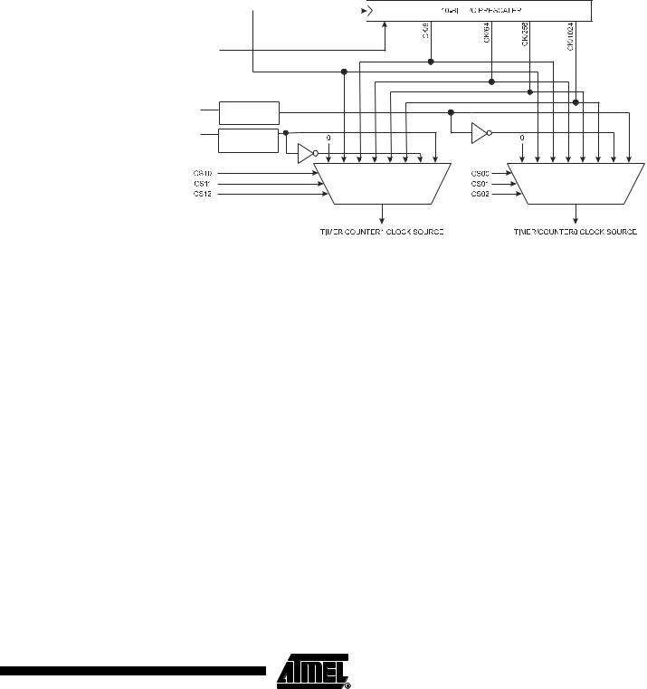
Timer/Counter1 and Timer/Counter0 share the same prescaler module, but the Timer/Counters can have different prescaler settings. The description below applies to both Timer/Counter1 and Timer/Counter0.
The Timer/Counter can be clocked directly by the system clock (by setting the CSn2:0 = 1). This provides the fastest operation, with a maximum Timer/Counter clock frequency equal to system clock frequency (fCLK_I/O). Alternatively, one of four taps from the prescaler can be used as a clock source. The prescaled clock has a frequency of either
fCLK_I/O/8, fCLK_I/O/64, fCLK_I/O/256, or fCLK_I/O/1024.
The prescaler is free running, i.e., operates independently of the clock select logic of the Timer/Counter, and it is shared by Timer/Counter1 and Timer/Counter0. Since the prescaler is not affected by the Timer/Counter’s clock select, the state of the prescaler will have implications for situations where a prescaled clock is used. One example of prescaling artifacts occurs when the timer is enabled and clocked by the prescaler (6 > CSn2:0 > 1). The number of system clock cycles from when the timer is enabled to the first count occurs can be from 1 to N+1 system clock cycles, where N equals the prescaler divisor (8, 64, 256, or 1024).
It is possible to use the Prescaler Reset for synchronizing the Timer/Counter to program execution. However, care must be taken if the other Timer/Counter that shares the same prescaler also uses prescaling. A prescaler reset will affect the prescaler period for all Timer/Counters it is connected to.
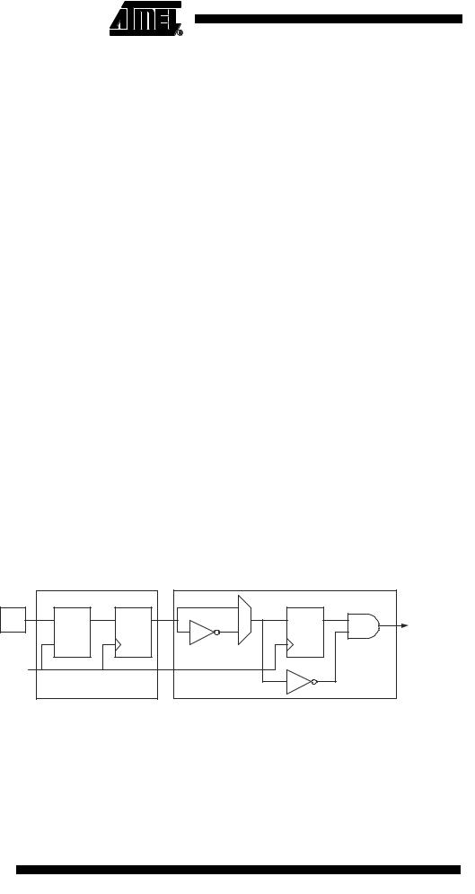
An external clock source applied to the T1/T0 pin can be used as Timer/Counter clock (clkT1/clkT0). The T1/T0 pin is sampled once every system clock cycle by the pin synchronization logic. The synchronized (sampled) signal is then passed through the edge detector. Figure 38 shows a functional equivalent block diagram of the T1/T0 synchronization and edge detector logic. The registers are clocked at the positive edge of the internal system clock (clkI/O). The latch is transparent in the high period of the internal system clock.
The edge detector generates one clkT1/clkT0 pulse for each positive (CSn2:0 = 7) or negative (CSn2:0 = 6) edge it detects.
Figure 38. T1/T0 Pin Sampling |
|
|
|
||||
Tn |
D |
Q |
D |
Q |
D |
Q |
Tn_sync |
|
|
|
|
|
|
|
(To Clock |
|
|
|
|
|
|
|
Select Logic) |
|
LE |
|
|
|
|
|
|
clkI/O |
|
|
|
|
|
|
|
|
|
|
Synchronization |
|
|
Edge Detector |
The synchronization and edge detector logic introduces a delay of 2.5 to 3.5 system clock cycles from an edge has been applied to the T1/T0 pin to the counter is updated.
Enabling and disabling of the clock input must be done when T1/T0 has been stable for at least one system clock cycle, otherwise it is a risk that a false Timer/Counter clock pulse is generated.
Each half period of the external clock applied must be longer than one system clock cycle to ensure correct sampling. The external clock must be guaranteed to have less
82 ATmega32(L)
2503F–AVR–12/03
ATmega32(L)
than half the system clock frequency (fExtClk < fclk_I/O/2) given a 50/50% duty cycle. Since the edge detector uses sampling, the maximum frequency of an external clock it can
detect is half the sampling frequency (Nyquist sampling theorem). However, due to variation of the system clock frequency and duty cycle caused by Oscillator source (crystal, resonator, and capacitors) tolerances, it is recommended that maximum frequency of an external clock source is less than fclk_I/O/2.5.
An external clock source can not be prescaled.
Figure 39. Prescaler for Timer/Counter0 and Timer/Counter1(1)
clkI/O
Clear
PSR10
T0
Synchronization
T1
Synchronization
Special Function IO Register –
SFIOR
|
|
|
clkT1 |
|
|
|
|
clkT0 |
|
|
Note: 1. |
The synchronization logic on the input pins (T1/T0) is shown in Figure 38. |
|
||||||||
Bit |
7 |
6 |
5 |
|
4 |
3 |
2 |
1 |
0 |
|
|
|
|
|
|
|
|
|
|
|
SFIOR |
|
ADTS2 |
ADTS1 |
ADTS0 |
|
– |
ACME |
PUD |
PSR2 |
PSR10 |
|
Read/Write |
R/W |
R/W |
R/W |
R |
R/W |
R/W |
R/W |
R/W |
|
|
Initial Value |
0 |
0 |
0 |
|
0 |
0 |
0 |
0 |
0 |
|
• Bit 0 – PSR10: Prescaler Reset Timer/Counter1 and Timer/Counter0
When this bit is written to one, the Timer/Counter1 and Timer/Counter0 prescaler will be reset. The bit will be cleared by hardware after the operation is performed. Writing a zero to this bit will have no effect. Note that Timer/Counter1 and Timer/Counter0 share the same prescaler and a reset of this prescaler will affect both timers. This bit will always be read as zero.
83
2503F–AVR–12/03