

Table 113. |
|
|
|
|
|
|
|
|
|
|
|
|
|
|
|
|
|
|
|
|
|
|
|
|
|
Parallel Programming Characteristics, VCC = 5 V ± 10% (Continued) |
|
|||||||||||
Symbol |
Parameter |
Min |
Typ |
Max |
|
Units |
||||||
|
|
|
|
|
|
|
|
|||||
tBVDV |
|
BS1 Valid to DATA valid |
0 |
|
250 |
|
ns |
|||||
tOLDV |
|
|
Low to DATA Valid |
|
|
250 |
|
ns |
||||
|
OE |
|
||||||||||
tOHDZ |
|
|
High to DATA Tri-stated |
|
|
250 |
|
ns |
||||
|
OE |
|
||||||||||
Notes: 1. tWLRH is valid for the Write Flash, Write EEPROM, Write Fuse bits and Write Lock bits commands.
2.tWLRH_CE is valid for the Chip Erase command.
SPI Serial Downloading Both the Flash and EEPROM memory arrays can be programmed using the serial SPI bus while RESET is pulled to GND. The serial interface consists of pins SCK, MOSI (input), and MISO (output). After RESET is set low, the Programming Enable instruction needs to be executed first before program/erase operations can be executed. NOTE, in Table 114 on page 268, the pin mapping for SPI programming is listed. Not all parts use the SPI pins dedicated for the internal SPI interface.
SPI Serial Programming |
|
|
|
|
|
|
|
|
|
|
|
|
|
|
Pin Mapping |
Table 114. Pin Mapping SPI Serial Programming |
|
|
|
||||||||||
|
|
|
|
|||||||||||
|
|
|
|
|
|
|
|
|
|
|
|
|
|
|
|
Symbol |
|
|
|
|
Pins |
|
|
I/O |
|
Description |
|||
|
|
|
|
|
|
|
|
|
|
|
|
|
|
|
|
MOSI |
|
|
|
|
PB5 |
|
|
I |
|
Serial Data in |
|||
|
|
|
|
|
|
|
|
|
|
|
|
|
|
|
|
MISO |
|
|
|
|
PB6 |
|
|
O |
|
Serial Data out |
|||
|
|
|
|
|
|
|
|
|
|
|
|
|
|
|
|
SCK |
|
|
|
|
PB7 |
|
|
I |
|
Serial Clock |
|||
|
|
|
|
|
|
|
|
|
|
|
|
|||
|
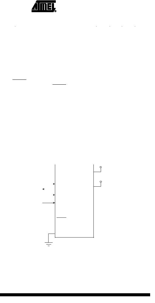
Figure 136. SPI Serial Programming and Verify(1) |
|||||||||||||
|
|
|
|
|
|
|
|
|
|
|
|
|
|
+2.7 - 5.5V |
|
|
|
|
|
|
|
|
|
|
|
|
|
|
|
|
|
|
|
|
|
|
|
|
|
|
|
VCC |
||
|
|
|
|
|
|
|
|
|
|
|
|
|
|
+2.7 - 5.5V(2) |
|
|
MOSI |
|
|
|
|
PB5 |
AVCC |
||||||
|
|
|
|
|
||||||||||
|
|
MISO |
|
|
|
PB6 |
||||||||
|
|
|
|
|
|
|
|
|||||||
|
|
|
|
|
|
|
||||||||
|
|
|
SCK |
|
|
|
|
PB7 |
|
|
|
|||
|
|
|
|
|
|
|
|
|||||||
|
|
|
|
|
|
|
|
|
|
XTAL1 |
|
|
|
|
|
|
|
|
|
|
|
|
|
|
|
|
|
||
 RESET
RESET
GND
Notes: 1. If the device is clocked by the Internal Oscillator, it is no need to connect a clock source to the XTAL1 pin.
2. VCC -0.3V < AVCC < VCC +0.3V, however, AVCC should always be within 2.7 - 5.5V
When programming the EEPROM, an auto-erase cycle is built into the self-timed programming operation (in the serial mode ONLY) and there is no need to first execute the
268 ATmega32(L)
2503F–AVR–12/03

 ATmega32(L)
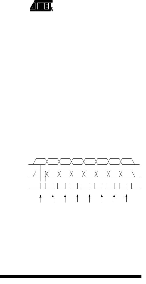
Data Polling Flash |
|
|
|
|
|
|
|
|
|
|
|
|
|
|
|
When a page is being programmed into the Flash, reading an address location within |
|||||||
|
the page being programmed will give the value $FF. At the time the device is ready for a |
||||||
|
new page, the programmed value will read correctly. This is used to determine when the |
||||||
|
next page can be written. Note that the entire page is written simultaneously and any |
||||||
|
address within the page can be used for polling. Data polling of the Flash will not work |
||||||
|
for the value $FF, so when programming this value, the user will have to wait for at least |
||||||
|
tWD_FLASH before programming the next page. As a chip erased device contains $FF in |
||||||
|
all locations, programming of addresses that are meant to contain $FF, can be skipped. |
||||||
|
See Table 115 for tWD_FLASH value |
||||||
Data Polling EEPROM |
When a new byte has been written and is being programmed into EEPROM, reading the |
||||||
|
address location being programmed will give the value $FF. At the time the device is |
||||||
|
ready for a new byte, the programmed value will read correctly. This is used to deter- |
||||||
|
mine when the next byte can be written. This will not work for the value $FF, but the user |
||||||
|
should have the following in mind: As a chip erased device contains $FF in all locations, |
||||||
|
programming of addresses that are meant to contain $FF, can be skipped. This does |
||||||
|
not apply if the EEPROM is re-programmed without chip erasing the device. In this |
||||||
|
case, data polling cannot be used for the value $FF, and the user will have to wait at |
||||||
|
least tWD_EEPROM before programming the next byte. See Table 115 for tWD_EEPROM |
||||||
|
value. |
|
|
|
|
|
|
|
Table 115. Minimum Wait Delay before Writing the Next Flash or EEPROM Location |
||||||
|
|
|
|
|
|
|
|
|
Symbol |
|
|
|
|
Minimum Wait Delay |
|
|
|
|
|
|
|
|
|
|
tWD_FLASH |
|
|
|
|
4.5 ms |
|
|
tWD_EEPROM |
|
|
|
|
9.0 ms |
|
|
tWD_ERASE |
|
|
|
|
9.0 ms |
|
|
Figure 137. SPI Serial Programming Waveforms |
||||||
|
SERIAL DATA INPUT |
MSB |
|
|
|
|
LSB |
|
(MOSI) |
|
|
|
|
|
|
|
SERIAL DATA OUTPUT |
MSB |
|
|
|
|
LSB |
|
(MISO) |
|
|
|
|
|
|
SERIAL CLOCK INPUT (SCK)
SAMPLE
270 ATmega32(L)
2503F–AVR–12/03
ATmega32(L)
Table 116. SPI Serial Programming Instruction Set
|
|
|
Instruction Format |
|
|
|
|
|
|
|
|
|
|
|
|
|
|
Instruction |
Byte 1 |
Byte 2 |
Byte 3 |
Byte4 |
|
Operation |
||
|
|
|
|
|
|
|
|
|
Programming Enable |
1010 1100 |
0101 0011 |
xxxx xxxx |
xxxx xxxx |
|
Enable SPI Serial Programming after |
||
|
|
|
|
|
|
|
||
|
|
|
|
|
RESET goes low. |
|||
|
|
|
|
|
|
|
||
|
|
|
|
|
|
|
|
|
Chip Erase |
1010 1100 |
100x xxxx |
xxxx xxxx |
xxxx xxxx |
|
Chip Erase EEPROM and Flash. |
||
|
|
|
|
|
|
|
|
|
Read Program Memory |
0010 H000 |
00aa aaaa |
bbbb bbbb |
oooo oooo |
|
Read H (high or low) data o from |
||
|
|
|
|
|
Program memory at word address a:b. |
|||
|
|
|
|
|
|
|
||
|
|
|
|
|
|
|
|
|
|
|
0100 H000 |
00xx xxxx |
xxbb bbbb |
iiii iiii |
|
Write H (high or low) data i to Program |
|
|
|
|
|
|
|
|
Memory page at word address b. Data |
|
Load Program Memory Page |
|
|
|
|
|
low byte must be loaded before Data |
||
|
|
|
|
|
|
|
high byte is applied within the same |
|
|
|
|
|
|
|
|
address. |
|
|
|
|
|
|
|
|
|
|
Write Program Memory Page |
0100 1100 |
00aa aaaa |
bbxx xxxx |
xxxx xxxx |
|
Write Program Memory Page at |
||
|
|
|
|
|
address a:b. |
|||
|
|
|
|
|
|
|
||
|
|
|
|
|
|
|
|
|
Read EEPROM Memory |
1010 0000 |
00xx xxaa |
bbbb bbbb |
oooo oooo |
|
Read data o from EEPROM memory at |
||
|
|
|
|
|
address a:b. |
|||
|
|
|
|
|
|
|
||
|
|
|
|
|
|
|
|
|
Write EEPROM Memory |
1100 0000 |
00xx xxaa |
bbbb bbbb |
iiii iiii |
|
Write data i to EEPROM memory at |
||
|
|
|
|
|
address a:b. |
|||
|
|
|
|
|
|
|
||
|
|
|
|
|
|
|
|
|
|
|
0101 1000 |
0000 0000 |
xxxx xxxx |
xxoo oooo |
|
Read Lock bits. “0” = programmed, “1” |
|
Read Lock Bits |
|
|
|
|
|
= unprogrammed. See Table 103 on |
||
|
|
|
|
|
|
|
page 254 for details. |
|
|
|
|
|
|
|
|
|
|
|
|
1010 1100 |
111x xxxx |
xxxx xxxx |
11ii iiii |
|
Write Lock bits. Set bits = “0” to |
|
Write Lock Bits |
|
|
|
|
|
program Lock bits. See Table 103 on |
||
|
|
|
|
|
|
|
page 254 for details. |
|
|
|
|
|
|
|
|
||
Read Signature Byte |
0011 0000 |
00xx xxxx |
xxxx xxbb |
oooo oooo |
|
Read Signature Byte o at address b. |
||
|
|
|
|
|
|
|
|
|
|
|
1010 1100 |
1010 0000 |
xxxx xxxx |
iiii iiii |
|
Set bits = “0” to program, “1” to |
|
Write Fuse Bits |
|
|
|
|
|
unprogram. See Table 106 on page |
||
|
|
|
|
|
|
|
256 for details. |
|
|
|
|
|
|
|
|
|
|
|
|
1010 1100 |
1010 1000 |
xxxx xxxx |
iiii iiii |
|
Set bits = “0” to program, “1” to |
|
Write Fuse High Bits |
|
|
|
|
|
unprogram. See Table 105 on page |
||
|
|
|
|
|
|
|
255 for details. |
|
|
|
|
|
|
|
|
|
|
|
|
0101 0000 |
0000 0000 |
xxxx xxxx |
oooo oooo |
|
Read Fuse bits. “0” = programmed, “1” |
|
Read Fuse Bits |
|
|
|
|
|
= unprogrammed. See Table 106 on |
||
|
|
|
|
|
|
|
page 256 for details. |
|
|
|
|
|
|
|
|
|
|
|
|
0101 1000 |
0000 1000 |
xxxx xxxx |
oooo oooo |
|
Read Fuse high bits. “0” = pro- |
|
Read Fuse High Bits |
|
|
|
|
|
grammed, “1” = unprogrammed. See |
||
|
|
|
|
|
|
|
Table 105 on page 255 for details. |
|
|
|
|
|
|
|
|
||
Read Calibration Byte |
0011 1000 |
00xx xxxx |
0000 0000 |
oooo oooo |
|
Read Calibration Byte |
||
|
|
|
|
|
|
|
|
|
Note: a = address high bits b = address low bits
H = 0 – Low byte, 1 – High Byte o = data out
i = data in
x = don’t care
271
2503F–AVR–12/03

SPI Serial Programming |
|
|
|
|
|
|
|
|
|
|
|
For Characteristics of SPI module, see “SPI Timing Characteristics” on page 289. |
|||||
Characteristics |
|
|
|
|
|
Programming via the |
Programming through the JTAG interface requires control of the four JTAG specific |
||||
JTAG Interface |
pins: TCK, TMS, TDI and TDO. Control of the reset and clock pins is not required. |
||||
|
To be able to use the JTAG interface, the JTAGEN Fuse must be programmed. The |
||||
|
device is default shipped with the fuse programmed. In addition, the JTD bit in MCUCSR |
||||
|
must be cleared. Alternatively, if the JTD bit is set, the External Reset can be forced low. |
||||
|
Then, the JTD bit will be cleared after two chip clocks, and the JTAG pins are available |
||||
|
for programming. This provides a means of using the JTAG pins as normal port pins in |
||||
|
running mode while still allowing In-System Programming via the JTAG interface. Note |
||||
|
that this technique can not be used when using the JTAG pins for Boundary-scan or On- |
||||
|
chip Debug. In these cases the JTAG pins must be dedicated for this purpose. |
||||
|
As a definition in this datasheet, the LSB is shifted in and out first of all Shift Registers. |
||||
Programming Specific JTAG |
The instruction register is 4-bit wide, supporting up to 16 instructions. The JTAG instruc- |
||||
Instructions |
tions useful for Programming are listed below. |
||||
|
The OPCODE for each instruction is shown behind the instruction name in hex format. |
||||
|
The text describes which Data Register is selected as path between TDI and TDO for |
||||
|
each instruction. |
||||
|
The Run-Test/Idle state of the TAP controller is used to generate internal clocks. It can |
||||
|
also be used as an idle state between JTAG sequences. The state machine sequence |
||||
|
for changing the instruction word is shown in Figure 138. |
||||
272 ATmega32(L)
2503F–AVR–12/03