


|
|
|
|
ATmega32(L) |
|
|
|
|
|
|
Analog Comparator |
|
|
|
|
When entering Idle mode, the Analog Comparator should be disabled if not used. When |
|||
|
||||
|
|
entering ADC Noise Reduction mode, the Analog Comparator should be disabled. In the |
||
|
|
other sleep modes, the Analog Comparator is automatically disabled. However, if the |
||
|
|
Analog Comparator is set up to use the Internal Voltage Reference as input, the Analog |
||
|
|
Comparator should be disabled in all sleep modes. Otherwise, the Internal Voltage Ref- |
||
|
|
erence will be enabled, independent of sleep mode. Refer to “Analog Comparator” on |
||
|
|
page 196 for details on how to configure the Analog Comparator. |
||
|
Brown-out Detector |
If the Brown-out Detector is not needed in the application, this module should be turned |
||
|
|
off. If the Brown-out Detector is enabled by the BODEN Fuse, it will be enabled in all |
||
|
|
sleep modes, and hence, always consume power. In the deeper sleep modes, this will |
||
|
|
contribute significantly to the total current consumption. Refer to “Brown-out Detection” |
||
|
|
on page 37 for details on how to configure the Brown-out Detector. |
||
|
Internal Voltage Reference |
The Internal Voltage Reference will be enabled when needed by the Brown-out Detec- |
||
|
|
tor, the Analog Comparator or the ADC. If these modules are disabled as described in |
||
|
|
the sections above, the internal voltage reference will be disabled and it will not be con- |
||
|
|
suming power. When turned on again, the user must allow the reference to start up |
||
|
|
before the output is used. If the reference is kept on in sleep mode, the output can be |
||
|
|
used immediately. Refer to “Internal Voltage Reference” on page 39 for details on the |
||
|
|
start-up time. |
||
|
Watchdog Timer |
If the Watchdog Timer is not needed in the application, this module should be turned off. |
||
|
|
If the Watchdog Timer is enabled, it will be enabled in all sleep modes, and hence, |
||
|
|
always consume power. In the deeper sleep modes, this will contribute significantly to |
||
|
|
the total current consumption. Refer to “Watchdog Timer” on page 39 for details on how |
||
|
|
to configure the Watchdog Timer. |
||
|
Port Pins |
When entering a sleep mode, all port pins should be configured to use minimum power. |
||
|
|
The most important thing is then to ensure that no pins drive resistive loads. In sleep |
||
|
|
modes where the both the I/O clock (clkI/O) and the ADC clock (clkADC) are stopped, the |
||
|
|
input buffers of the device will be disabled. This ensures that no power is consumed by |
||
|
|
the input logic when not needed. In some cases, the input logic is needed for detecting |
||
|
|
wake-up conditions, and it will then be enabled. Refer to the section “Digital Input |
||
|
|
Enable and Sleep Modes” on page 51 for details on which pins are enabled. If the input |
||
|
|
buffer is enabled and the input signal is left floating or have an analog signal level close |
||
|
|
to VCC/2, the input buffer will use excessive power. |
||
|
JTAG Interface and On-chip |
If the On-chip debug system is enabled by the OCDEN Fuse and the chip enter Power |
||
|
Debug System |
down or Power save sleep mode, the main clock source remains enabled. In these |
||
|
|
sleep modes, this will contribute significantly to the total current consumption. There are |
||
|
|
three alternative ways to avoid this: |
||
|
|
• |
Disable OCDEN Fuse. |
|
|
|
• |
Disable JTAGEN Fuse. |
|
|
|
• Write one to the JTD bit in MCUCSR. |
||
The TDO pin is left floating when the JTAG interface is enabled while the JTAG TAP controller is not shifting data. If the hardware connected to the TDO pin does not pull up the logic level, power consumption will increase. Note that the TDI pin for the next device in the scan chain contains a pull-up that avoids this problem. Writing the JTD bit in the MCUCSR register to one or leaving the JTAG fuse unprogrammed disables the JTAG interface.
33
2503F–AVR–12/03

System Control and
Reset
Resetting the AVR |
During Reset, all I/O Registers are set to their initial values, and the program starts exe- |
||
|
cution from the Reset Vector. The instruction placed at the Reset Vector must be a JMP |
||
|
– absolute jump – instruction to the reset handling routine. If the program never enables |
||
|
an interrupt source, the Interrupt Vectors are not used, and regular program code can |
||
|
be placed at these locations. This is also the case if the Reset Vector is in the Applica- |
||
|
tion section while the Interrupt Vectors are in the Boot section or vice versa. The circuit |
||
|
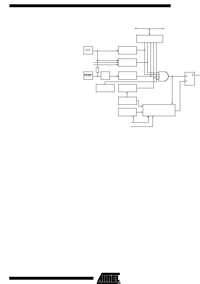
diagram in Figure 15 shows the reset logic. Table 15 defines the electrical parameters of |
||
|
the reset circuitry. |
||
|
The I/O ports of the AVR are immediately reset to their initial state when a reset source |
||
|
goes active. This does not require any clock source to be running. |
||
|
After all reset sources have gone inactive, a delay counter is invoked, stretching the |
||
|
Internal Reset. This allows the power to reach a stable level before normal operation |
||
|
starts. The time-out period of the delay counter is defined by the user through the |
||
|
CKSEL Fuses. The different selections for the delay period are presented in “Clock |
||
|
Sources” on page 23. |
||
Reset Sources |
The ATmega32 has five sources of reset: |
||
|
• Power-on Reset. The MCU is reset when the supply voltage is below the Power-on |
||
|
Reset threshold (VPOT). |
||
|
• External Reset. The MCU is reset when a low level is present on the |
|
pin for |
|
RESET |
||
|
longer than the minimum pulse length. |
||
|
• Watchdog Reset. The MCU is reset when the Watchdog Timer period expires and |
||
|
the Watchdog is enabled. |
||
|
• Brown-out Reset. The MCU is reset when the supply voltage VCC is below the |
||
|
Brown-out Reset threshold (VBOT) and the Brown-out Detector is enabled. |
||
|
• JTAG AVR Reset. The MCU is reset as long as there is a logic one in the Reset |
||
|
Register, one of the scan chains of the JTAG system. Refer to the section “IEEE |
||
|
1149.1 (JTAG) Boundary-scan” on page 223 for details. |
||
34 ATmega32(L)
2503F–AVR–12/03
|
|
|
|
|
ATmega32(L) |
Figure 15. |
Reset Logic |
|
|
|
|
|
|
|
|
DATA BUS |
|
|
|
|
MCU Control and Status |
|
|
|
|
|
Register (MCUCSR) |
|
|
|
|
Power-on |
|
PORF BORF EXTRF WDRF JTRF |
|
|
|
Reset Circuit |
|
|
|
BODEN |
Brown-out |
|
|
|
|
Reset Circuit |
|
|
|
||
BODLEVEL |
|
|
RESET |
||
|
|
|
|||
|
Pull-up Resistor |
|
|
|
|
|
JTAG Reset |
Watchdog |
|
RESET |
INTERNAL |
|
SPIKE |
Reset Circuit |
|
|
|
|
FILTER |
|
|
|
|
|
Register |
Timer |
|
COUNTER |
|
|
|
Watchdog |
|
|
|
|
|
Oscillator |
|
|
|
|
|
Clock |
CK |
Delay Counters |
TIMEOUT |
|
|
Generator |
|
|
|
|
|
CKSEL[3:0] |
|
|
|
|
|
SUT[1:0] |
|
|
|
Table 15. |
Reset Characteristics |
|
|
|
|
Symbol |
|
Parameter |
Condition |
Min |
Typ |
Max |
Units |
||
|
|
|
|
|
|
|
|
||
|
|
Power-on Reset |
|
|
1.4 |
2.3 |
V |
||
|
|
Threshold Voltage (rising) |
|
|
|||||
|
|
|
|
|
|
|
|||
VPOT |
|
|
|
|
|
|
|
||
|
Power-on Reset |
|
|
|
|
|
|||
|
|
Threshold Voltage |
|
|
1.3 |
2.3 |
V |
||
|
|
(falling)(1) |
|
|
|
|
|
||
|
|
|
|
Pin Threshold |
|
|
|
|
|
VRST |
|
RESET |
|
0.1 VCC |
|
0.9VCC |
V |
||
|
Voltage |
|
|
||||||
tRST |
|
Minimum pulse width on |
|
|
|
1.5 |
µs |
||
|
|
Pin |
|
|
|
||||
RESET |
|
|
|
||||||
VBOT |
|
Brown-out Reset |
BODLEVEL = 1 |
2.5 |
2.7 |
3.2 |
V |
||
|
Threshold Voltage(2) |
|
|
|
|
||||
|
BODLEVEL = 0 |
3.7 |
4.0 |
4.2 |
|||||
|
|
|
|
|
|
||||
|
|
|
|
|
|
|
|
||
|
|
Minimum low voltage |
BODLEVEL = 1 |
|
2 |
|
µs |
||
tBOD |
|
period for Brown-out |
|
|
|
|
|
||
|
BODLEVEL = 0 |
|
2 |
|
µs |
||||
|
|
Detection |
|
|
|||||
|
|
|
|
|
|
|
|
||
VHYST |
|
Brown-out Detector |
|
|
50 |
|
mV |
||
|
hysteresis |
|
|
|
|||||
|
|
|
|
|
|
|
|||
|
|
|
|
|
|
|
|
|
|
Notes: 1. The Power-on Reset will not work unless the supply voltage has been below VPOT (falling).
2.VBOT may be below nominal minimum operating voltage for some devices. For devices where this is the case, the device is tested down to VCC = VBOT during the production test. This guarantees that a Brown-out Reset will occur before VCC drops to a voltage where correct operation of the microcontroller is no longer guaranteed. The test is performed using BODLEVEL = 1 for ATmega32L and BODLEVEL = 0 for ATmega32. BODLEVEL = 1 is not applicable for ATmega32.
35
2503F–AVR–12/03
Power-on Reset |
|
|
|
|
|
|
|
|
|
|
|
|
|
|
|
|
|
|
|
|
|
|
|
|
|
|
|
|
|
|
|
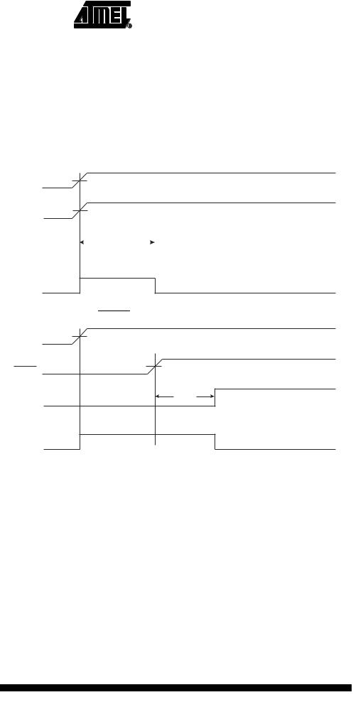
A Power-on Reset (POR) pulse is generated by an On-chip detection circuit. The detec- |
|||||||||||||||
|
tion level is defined in Table 15. The POR is activated whenever VCC is below the |
||||||||||||||
|
detection level. The POR circuit can be used to trigger the Start-up Reset, as well as to |
||||||||||||||
|
detect a failure in supply voltage. |
||||||||||||||
|
A Power-on Reset (POR) circuit ensures that the device is reset from Power-on. Reach- |
||||||||||||||
|
ing the Power-on Reset threshold voltage invokes the delay counter, which determines |
||||||||||||||
|
how long the device is kept in RESET after VCC rise. The RESET signal is activated |
||||||||||||||
|
again, without any delay, when VCC decreases below the detection level. |
||||||||||||||
|
Figure 16. MCU Start-up, |
|
|
|
Tied to VCC. |
||||||||||
|
RESET |
||||||||||||||
|
|
VCC |
|
VPOT |
|||||||||||
|
|
|
|
|
|
|
|
|
|
|
|
|
|
||
|
|
|
|
|
VRST |
||||||||||
|
|
RESET |
|||||||||||||
|
|
|
|
|
|
|
|
|
|
|
|
|
|
||
|
TIME-OUT |
|
|
|
tTOUT |
|
|
|
|
||||||
|
|
|
|
|
|
|
|||||||||
|
|
|
|
|
|
|
|||||||||
INTERNAL
RESET
Figure 17. MCU Start-up, RESET Extended Externally
VPOT
VCC
VRST
RESET
tTOUT
TIME-OUT
INTERNAL
RESET
36 ATmega32(L)
2503F–AVR–12/03