


|
|
|
|
|
|
|
|
|
|
|
|
|
The receive function example reads all the I/O Registers into the Register File before |
||||
|
any computation is done. This gives an optimal receive buffer utilization since the buffer |
||||
|
location read will be free to accept new data as early as possible. |
||||
Receive Compete Flag and |
The USART Receiver has one flag that indicates the receiver state. |
||||
Interrupt |
The Receive Complete (RXC) Flag indicates if there are unread data present in the |
||||
|
|||||
|
receive buffer. This flag is one when unread data exist in the receive buffer, and zero |
||||
|
when the receive buffer is empty (i.e., does not contain any unread data). If the receiver |
||||
|
is disabled (RXEN = 0), the receive buffer will be flushed and consequently the RXC bit |
||||
|
will become zero. |
||||
|
When the Receive Complete Interrupt Enable (RXCIE) in UCSRB is set, the USART |
||||
|
Receive Complete Interrupt will be executed as long as the RXC Flag is set (provided |
||||
|
that global interrupts are enabled). When interrupt-driven data reception is used, the |
||||
|
receive complete routine must read the received data from UDR in order to clear the |
||||
|
RXC Flag, otherwise a new interrupt will occur once the interrupt routine terminates. |
||||
Receiver Error Flags |
The USART Receiver has three Error Flags: Frame Error (FE), Data OverRun (DOR) |
||||
|
and Parity Error (PE). All can be accessed by reading UCSRA. Common for the Error |
||||
|
Flags is that they are located in the receive buffer together with the frame for which they |
||||
|
indicate the error status. Due to the buffering of the Error Flags, the UCSRA must be |
||||
|
read before the receive buffer (UDR), since reading the UDR I/O location changes the |
||||
|
buffer read location. Another equality for the Error Flags is that they can not be altered |
||||
|
by software doing a write to the flag location. However, all flags must be set to zero |
||||
|
when the UCSRA is written for upward compatibility of future USART implementations. |
||||
|
None of the Error Flags can generate interrupts. |
||||
|
The Frame Error (FE) Flag indicates the state of the first stop bit of the next readable |
||||
|
frame stored in the receive buffer. The FE Flag is zero when the stop bit was correctly |
||||
|
read (as one), and the FE Flag will be one when the stop bit was incorrect (zero). This |
||||
|
flag can be used for detecting out-of-sync conditions, detecting break conditions and |
||||
|
protocol handling. The FE Flag is not affected by the setting of the USBS bit in UCSRC |
||||
|
since the receiver ignores all, except for the first, stop bits. For compatibility with future |
||||
|
devices, always set this bit to zero when writing to UCSRA. |
||||
|
The Data OverRun (DOR) Flag indicates data loss due to a receiver buffer full condition. |
||||
|
A Data OverRun occurs when the receive buffer is full (two characters), it is a new char- |
||||
|
acter waiting in the receive Shift Register, and a new start bit is detected. If the DOR |
||||
|
Flag is set there was one or more serial frame lost between the frame last read from |
||||
|
UDR, and the next frame read from UDR. For compatibility with future devices, always |
||||
|
write this bit to zero when writing to UCSRA. The DOR Flag is cleared when the frame |
||||
|
received was successfully moved from the Shift Register to the receive buffer. |
||||
|
The Parity Error (PE) Flag indicates that the next frame in the receive buffer had a parity |
||||
|
error when received. If parity check is not enabled the PE bit will always be read zero. |
||||
|
For compatibility with future devices, always set this bit to zero when writing to UCSRA. |
||||
|
For more details see “Parity Bit Calculation” on page 143 and “Parity Checker” on page |
||||
|
150. |
|
|
|
|
Parity Checker |
The Parity Checker is active when the high USART Parity mode (UPM1) bit is set. Type |
||||
|
of parity check to be performed (odd or even) is selected by the UPM0 bit. When |
||||
|
enabled, the parity checker calculates the parity of the data bits in incoming frames and |
||||
|
compares the result with the parity bit from the serial frame. The result of the check is |
||||
|
stored in the receive buffer together with the received data and stop bits. The Parity |
||||
|
Error (PE) Flag can then be read by software to check if the frame had a parity error. |
||||
150 ATmega32(L)
2503F–AVR–12/03
|
|
|
ATmega32(L) |
|
|
|
|
|
|
|
|
|
|
The PE bit is set if the next character that can be read from the receive buffer had a par- |
|
|
|
||
|
|
ity error when received and the parity checking was enabled at that point (UPM1 = 1). |
|
|
|
This bit is valid until the receive buffer (UDR) is read. |
|
|
Disabling the Receiver |
In contrast to the Transmitter, disabling of the Receiver will be immediate. Data from |
|
|
|
ongoing receptions will therefore be lost. When disabled (i.e., the RXEN is set to zero) |
|
|
|
the Receiver will no longer override the normal function of the RxD port pin. The receiver |
|
|
|
buffer FIFO will be flushed when the receiver is disabled. Remaining data in the buffer |
|
|
|
will be lost |
|
Flushing the Receive Buffer
Asynchronous Data
Reception
The receiver buffer FIFO will be flushed when the Receiver is disabled, i.e., the buffer will be emptied of its contents. Unread data will be lost. If the buffer has to be flushed during normal operation, due to for instance an error condition, read the UDR I/O location until the RXC Flag is cleared. The following code example shows how to flush the receive buffer.
Assembly Code Example(1)
USART_Flush:
sbis UCSRA, RXC
ret
in r16, UDR rjmp USART_Flush
C Code Example(1)
void USART_Flush( void )
{
unsigned char dummy;
while ( UCSRA & (1<<RXC) ) dummy = UDR;
}
Note: 1. The example code assumes that the part specific header file is included.
The USART includes a clock recovery and a data recovery unit for handling asynchronous data reception. The clock recovery logic is used for synchronizing the internally generated baud rate clock to the incoming asynchronous serial frames at the RxD pin. The data recovery logic samples and low pass filters each incoming bit, thereby improving the noise immunity of the receiver. The asynchronous reception operational range depends on the accuracy of the internal baud rate clock, the rate of the incoming frames, and the frame size in number of bits.
Asynchronous Clock |
The clock recovery logic synchronizes internal clock to the incoming serial frames. Fig- |
Recovery |
ure 73 illustrates the sampling process of the start bit of an incoming frame. The sample |
|
rate is 16 times the baud rate for Normal mode, and 8 times the baud rate for Double |
|
Speed mode. The horizontal arrows illustrate the synchronization variation due to the |
|
sampling process. Note the larger time variation when using the double speed mode |
|
(U2X = 1) of operation. Samples denoted zero are samples done when the RxD line is |
|
idle (i.e., no communication activity). |
151
2503F–AVR–12/03
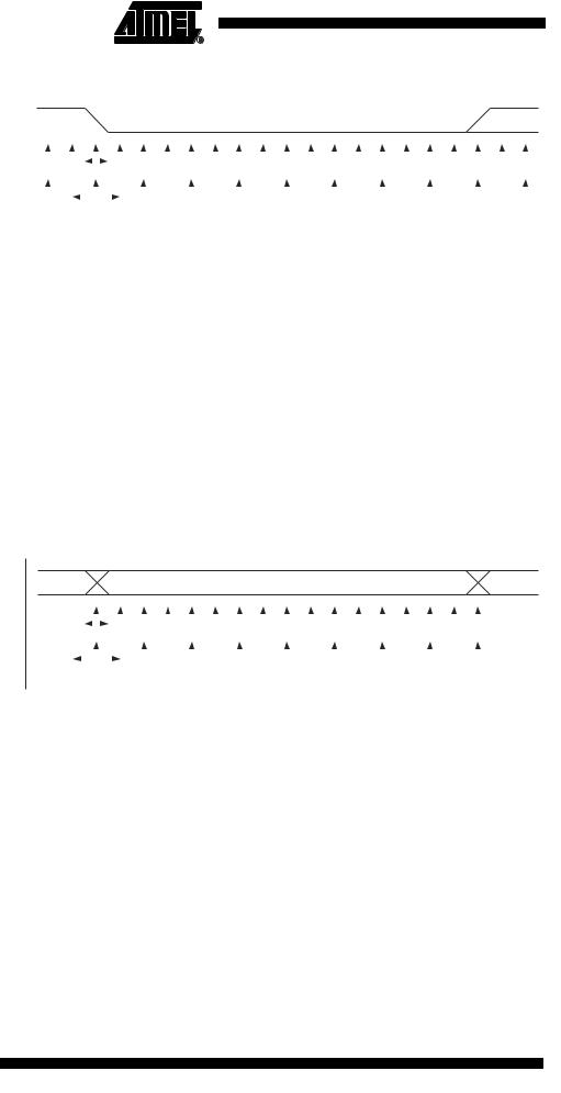
Figure 73. Start Bit Sampling
RxD |
|
IDLE |
|
|
|
|
|
|
|
|
|
|
|
|
|
|
|
|
|
|
|
START |
|
|
|
|
|
|
|
|
|
|
|
|
|
|
BIT 0 |
||||||||
Sample |
|
|
|
|
|
|
|
|
|
|
|
|
|
|
|
|
|
|
|
|
|
|
|
|
|
|
|
|
|
|
|
|
|
|
|
|
|
|
|
|
|
|
|
|
|
|
|
|
|
|
|
|
|
|
|
|
|
|
|
|
|
|
|
|
|
|
|
|
|
|
|
|
|
|
|
|
|
|
|
|
|
|
|
|
|
|
|
|
|
|
|
|
|
|
|
|
|
|
|
|
|
|
|
|
|
|
|
|
|
|
|
|
|
|
|
|
|
|
|
|
|
|
|
|
|
|
|
|
|
|
|
|
|
|
|
|
|
(U2X = 0) |
0 |
0 |
|
1 |
|
2 |
3 |
4 |
5 |
6 |
7 |
8 |
|
9 |
|
10 |
11 |
12 13 |
14 15 16 |
1 |
2 |
3 |
|||||||||||||||||||||||
Sample |
|
|
|
|
|
|
|
|
|
|
|
|
|
|
|
|
|
|
|
|
|
|
|
|
|
|
|
|
|
|
|
|
|
|
|
|
|
|
|
|
|
|
|
|
|
|
|
|
|
|
|
|
|
|
|
|
|
|
|
|
|
|
|
|
|
|
|
|
|
|
|
|
|
|
|
|
|
|
|
|
|
|
|
|
|
|
|
|
|
|
|
|
|
|
|
|
|
|
|
|
|
|
|
|
|
|
|
|
|
|
|
|
|
|
|
|
|
|
|
|
|
|
|
|
|
|
|
|
|
|
|
|
|
|
|
|
|
|
|
|
|
|
|
|
|
|
|
|
|
|
|
|
|
|
|
|
|
|
|
|
|
|
|
|
|
|
|
|
|
|
|
|
|
|
|
|
|
|
|
|
|
|
|
(U2X = 1) |
0 |
|
|
|
1 |
|
|
|
|
2 |
|
|
3 |
|
|
4 |
|
|
|
5 |
|
|
|
6 |
7 |
8 |
|
1 |
|
|
2 |
||||||||||||||
|
|
|
|
|
|
|
|
|
|
|
|
|
|
|
|
|
|
|
|
|
|
|
|
|
|
|
|
|
|
|
|
|
|
|
|
|
|
|
|
|
|
|
|
|
|
When the clock recovery logic detects a high (idle) to low (start) transition on the RxD line, the start bit detection sequence is initiated. Let sample 1 denote the first zero-sam- ple as shown in the figure. The clock recovery logic then uses samples 8, 9, and 10 for Normal mode, and samples 4, 5, and 6 for Double Speed mode (indicated with sample numbers inside boxes on the figure), to decide if a valid start bit is received. If two or more of these three samples have logical high levels (the majority wins), the start bit is rejected as a noise spike and the receiver starts looking for the next high to low-transi- tion. If however, a valid start bit is detected, the clock recovery logic is synchronized and the data recovery can begin. The synchronization process is repeated for each start bit.
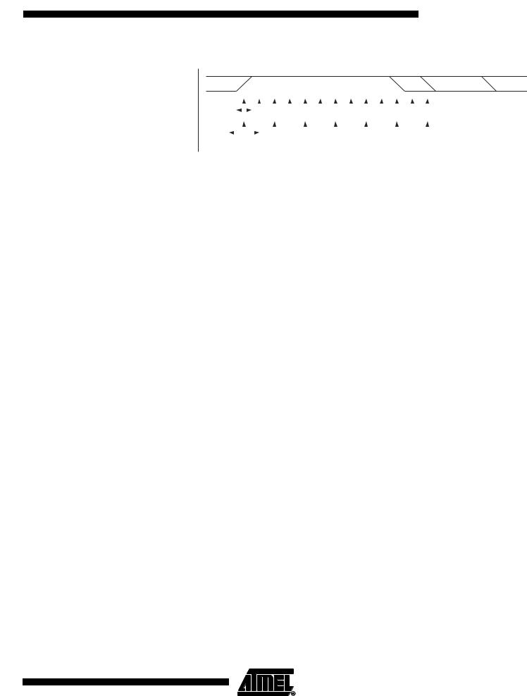
Asynchronous Data Recovery When the receiver clock is synchronized to the start bit, the data recovery can begin. The data recovery unit uses a state machine that has 16 states for each bit in normal mode and 8 states for each bit in Double Speed mode. Figure 74 shows the sampling of the data bits and the parity bit. Each of the samples is given a number that is equal to the state of the recovery unit.
Figure 74. Sampling of Data and Parity Bit
RxD |
|
|
|
|
|
|
|
|
|
|
|
|
|
|
|
|
|
|
|
BIT n |
|
|
|
|
|
|
|
|
|
|
|
|
|
|||||
Sample |
|
|
|
|
|
|
|
|
|
|
|
|
|
|
|
|
|
|
|
|
|
|
|
|
|
|
|
|
|
|
|
|
|
|
|
|
||
|
|
|
|
|
|
|
|
|
|
|
|
|
|
|
|
|
|
|
|
|
|
|
|
|
|
|
|
|
|
|
|
|
|
|
|
|||
|
|
|
|
|
|
|
|
|
|
|
|
|
|
|
|
|
|
|
|
|
|
|
|
|
|
|
|
|
|
|
|
|
|
|
|
|||
(U2X = 0) |
1 |
|
2 |
3 |
4 |
5 |
6 |
7 |
8 |
|
9 |
|
10 |
11 |
12 13 |
14 15 16 |
1 |
|||||||||||||||||||||
|
|
|
|
|
|
|
|
|
|
|
|
|
|
|
|
|
|
|
|
|
|
|
|
|
|
|
|
|
|
|
|
|
|
|
|
|
|
|
|
|
|
|
|
|
|
|
|
|
|
|
|
|
|
|
|
|
|
|
|
|
|
|
|
|
|
|
|
|
|
|
|
|
|
|
|
|
|
Sample |
|
|
|
|
|
|
|
|
|
|
|
|
|
|
|
|
|
|
|
|
|
|
|
|
|
|
|
|
|
|
|
|
|
|
|
|
|
|
|
|
|
|
|
|
|
|
|
|
|
|
|
|
|
|
|
|
|
|
|
|
|
|
|
|
|
|
|
|
|
|
|
|
|
|
|
|
|
(U2X = 1) |
1 |
|
|
|
|
2 |
|
|
3 |
|
|
4 |
|
|
|
5 |
|
|
|
6 |
7 |
8 |
|
1 |
||||||||||||||
The decision of the logic level of the received bit is taken by doing a majority voting of the logic value to the three samples in the center of the received bit. The center samples are emphasized on the figure by having the sample number inside boxes. The majority voting process is done as follows: If two or all three samples have high levels, the received bit is registered to be a logic 1. If two or all three samples have low levels, the received bit is registered to be a logic 0. This majority voting process acts as a low pass filter for the incoming signal on the RxD pin. The recovery process is then repeated until a complete frame is received. Including the first stop bit. Note that the receiver only uses the first stop bit of a frame.
Figure 75 shows the sampling of the stop bit and the earliest possible beginning of the start bit of the next frame.
152 ATmega32(L)
2503F–AVR–12/03
ATmega32(L)
Figure 75. Stop Bit Sampling and Next Start Bit Sampling
RxD |
|
|
|
|
|
|
|
|
|
|
|
|
|
|
|
|
|
|
|
STOP 1 |
|
|
(A) |
|
|
(B) |
|
(C) |
|||||||
Sample |
|
|
|
|
|
|
|
|
|
|
|
|
|
|
|
|
|
|
|
|
|
|
|
|
|
|
|
|
|
|
|
|
|
||
|
|
|
|
|
|
|
|
|
|
|
|
|
|
|
|
|
|
|
|
|
|
|
|
|
|
|
|
|
|
|
|
|
|||
|
|
|
|
|
|
|
|
|
|
|
|
|
|
|
|
|
|
|
|
|
|
|
|
|
|
|
|
|
|
|
|
|
|||
(U2X = 0) |
1 |
|
2 |
3 |
4 |
5 |
6 |
7 |
8 |
|
9 |
|
10 |
0/1 |
0/1 0/1 |
|
|
||||||||||||||||||
|
|
|
|
|
|
|
|
|
|
|
|
|
|
|
|
|
|
|
|
|
|
|
|
|
|
|
|
|
|
|
|
|
|
|
|
|
|
|
|
|
|
|
|
|
|
|
|
|
|
|
|
|
|
|
|
|
|
|
|
|
|
|
|
|
|
|
|
|
|
|
|
Sample |
|
|
|
|
|
|
|
|
|
|
|
|
|
|
|
|
|
|
|
|
|
|
|
|
|
|
|
|
|
|
|
|
|
|
|
|
|
|
|
|
|
|
|
|
|
|
|
|
|
|
|
|
|
|
|
|
|
|
|
|
|
|
|
|
|
|
|
|
|
|
|
(U2X = 1) |
1 |
|
|
|
|
2 |
|
|
3 |
|
|
4 |
|
|
|
5 |
|
|
6 |
0/1 |
|
|
|||||||||||||
|
The same majority voting is done to the stop bit as done for the other bits in the frame. If |
||
|
the stop bit is registered to have a logic 0 value, the Frame Error (FE) Flag will be set. |
||
|
A new high to low transition indicating the start bit of a new frame can come right after |
||
|
the last of the bits used for majority voting. For Normal Speed mode, the first low level |
||
|
sample can be at point marked (A) in Figure 75. For Double Speed mode the first low |
||
|
level must be delayed to (B). (C) marks a stop bit of full length. The early start bit detec- |
||
|
tion influences the operational range of the receiver. |
||
Asynchronous Operational |
The operational range of the receiver is dependent on the mismatch between the |
||
Range |
received bit rate and the internally generated baud rate. If the Transmitter is sending |
||
|
frames at too fast or too slow bit rates, or the internally generated baud rate of the |
||
|
receiver does not have a similar (see Table 61) base frequency, the receiver will not be |
||
|
able to synchronize the frames to the start bit. |
||
|
The following equations can be used to calculate the ratio of the incoming data rate and |
||
|
internal receiver baud rate. |
|
|
|
Rs l ow |
= |
(D + 1)S |
|
S-----–-----1----+-----D---------S-----+-----S---F- |
||
|
|
|
|
|
Rfa st |
= |
(D + 2)S |
|
(---D------+-----1---)---S----+-----S---M--- |
||
|
|
|
|
D Sum of character size and parity size (D = 5 to 10 bit)
SSamples per bit. S = 16 for Normal Speed mode and S = 8 for Double Speed mode.
SF |
First sample number used for majority voting. SF = 8 for Normal Speed and |
|
SF = 4 for Double Speed mode. |
SM |
Middle sample number used for majority voting. SM = 9 for Normal Speed and |
|
SM = 5 for Double Speed mode. |
Rslow is the ratio of the slowest incoming data rate that can be accepted in relation to the receiver baud rate. Rfast is the ratio of the fastest incoming data rate that can be accepted in relation to the receiver baud rate.
153
2503F–AVR–12/03
Table 61 and Table 62 list the maximum receiver baud rate error that can be tolerated.
Note that Normal Speed mode has higher toleration of baud rate variations.
Table 61. Recommended Maximum Receiver Baud Rate Error for Normal Speed Mode (U2X = 0)
D |
|
|
Max Total |
Recommended Max |
# (Data+Parity Bit) |
Rslow (%) |
Rfast(%) |
Error (%) |
Receiver Error (%) |
5 |
93.20 |
106.67 |
+6.67/-6.8 |
± 3.0 |
|
|
|
|
|
6 |
94.12 |
105.79 |
+5.79/-5.88 |
± 2.5 |
|
|
|
|
|
7 |
94.81 |
105.11 |
+5.11/-5.19 |
± 2.0 |
|
|
|
|
|
8 |
95.36 |
104.58 |
+4.58/-4.54 |
± 2.0 |
|
|
|
|
|
9 |
95.81 |
104.14 |
+4.14/-4.19 |
± 1.5 |
|
|
|
|
|
10 |
96.17 |
103.78 |
+3.78/-3.83 |
± 1.5 |
|
|
|
|
|
Table 62. Recommended Maximum Receiver Baud Rate Error for Double Speed Mode (U2X = 1)
D |
|
|
Max Total |
Recommended Max |
# (Data+Parity Bit) |
Rslow (%) |
Rfast (%) |
Error (%) |
Receiver Error (%) |
5 |
94.12 |
105.66 |
+5.66/-5.88 |
± 2.5 |
|
|
|
|
|
6 |
94.92 |
104.92 |
+4.92/-5.08 |
± 2.0 |
|
|
|
|
|
7 |
95.52 |
104.35 |
+4.35/-4.48 |
± 1.5 |
|
|
|
|
|
8 |
96.00 |
103.90 |
+3.90/-4.00 |
± 1.5 |
|
|
|
|
|
9 |
96.39 |
103.53 |
+3.53/-3.61 |
± 1.5 |
|
|
|
|
|
10 |
96.70 |
103.23 |
+3.23/-3.30 |
± 1.0 |
|
|
|
|
|
The recommendations of the maximum receiver baud rate error was made under the assumption that the receiver and transmitter equally divides the maximum total error.
There are two possible sources for the receivers baud rate error. The receiver’s system clock (XTAL) will always have some minor instability over the supply voltage range and the temperature range. When using a crystal to generate the system clock, this is rarely a problem, but for a resonator the system clock may differ more than 2% depending of the resonators tolerance. The second source for the error is more controllable. The baud rate generator can not always do an exact division of the system frequency to get the baud rate wanted. In this case an UBRR value that gives an acceptable low error can be used if possible.
154 ATmega32(L)
2503F–AVR–12/03