
PROG_COMMANDS ($5) |
|
|
|
|
|
|
|
|
|
|
|
|
|
|
|
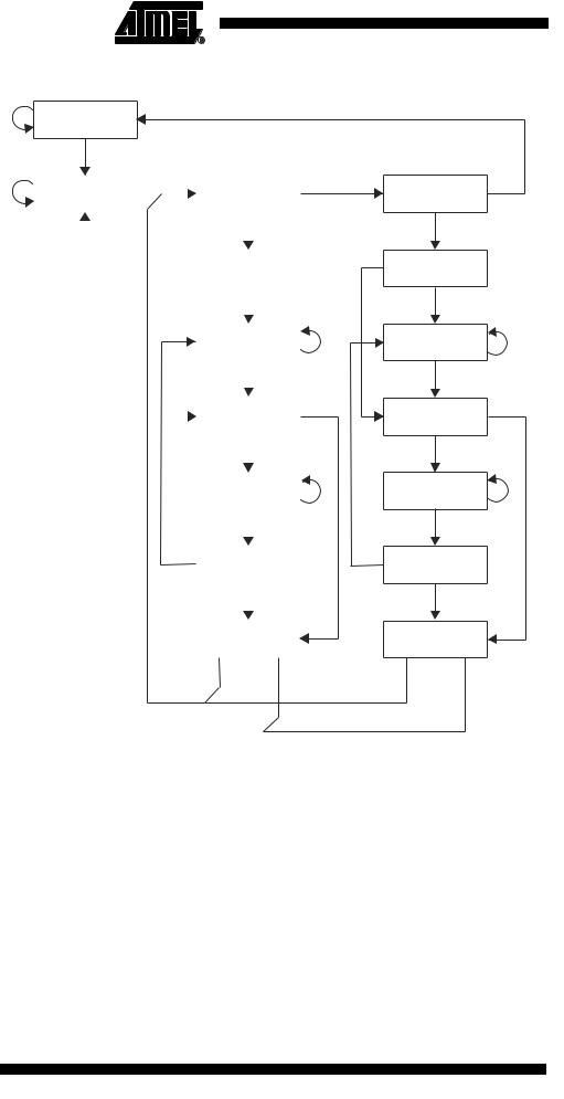
The AVR specific public JTAG instruction for entering programming commands via the |
|||||||
|
JTAG port. The 15-bit Programming Command Register is selected as Data Register. |
||||||
|
The active states are the following: |
||||||
|
• Capture-DR: The result of the previous command is loaded into the Data Register. |
||||||
|
• Shift-DR: The Data Register is shifted by the TCK input, shifting out the result of the |
||||||
|
|
previous command and shifting in the new command. |
|||||
|
• Update-DR: The programming command is applied to the Flash inputs |
||||||
|
• Run-Test/Idle: One clock cycle is generated, executing the applied command (not |
||||||
|
|
always required, see Table 117 below). |
|||||
PROG_PAGELOAD ($6) |
The AVR specific public JTAG instruction to directly load the Flash data page via the |
||||||
|
JTAG port. The 1024 bit Virtual Flash Page Load Register is selected as Data Register. |
||||||
|
This is a virtual scan chain with length equal to the number of bits in one Flash page. |
||||||
|
Internally the Shift Register is 8-bit. Unlike most JTAG instructions, the Update-DR state |
||||||
|
is not used to transfer data from the Shift Register. The data are automatically trans- |
||||||
|
ferred to the Flash page buffer byte by byte in the Shift-DR state by an internal state |
||||||
|
machine. This is the only active state: |
||||||
|
• Shift-DR: Flash page data are shifted in from TDI by the TCK input, and |
||||||
|
|
automatically loaded into the Flash page one byte at a time. |
|||||
|
Note: |
The JTAG instruction PROG_PAGELOAD can only be used if the AVR device is the first |
|||||
|
|
|
device in JTAG scan chain. If the AVR cannot be the first device in the scan chain, the |
||||
|
|
|
byte-wise programming algorithm must be used. |
||||
PROG_PAGEREAD ($7) |
The AVR specific public JTAG instruction to read one full Flash data page via the JTAG |
||||||
|
port. The 1032 bit Virtual Flash Page Read Register is selected as Data Register. This is |
||||||
|
a virtual scan chain with length equal to the number of bits in one Flash page plus 8. |
||||||
|
Internally the Shift Register is 8-bit. Unlike most JTAG instructions, the Capture-DR |
||||||
|
state is not used to transfer data to the Shift Register. The data are automatically trans- |
||||||
|
ferred from the Flash page buffer byte by byte in the Shift-DR state by an internal state |
||||||
|
machine. This is the only active state: |
||||||
|
• Shift-DR: Flash data are automatically read one byte at a time and shifted out on |
||||||
|
|
TDO by the TCK input. The TDI input is ignored. |
|||||
|
Note: |
The JTAG instruction PROG_PAGEREAD can only be used if the AVR device is the first |
|||||
|
|
|
device in JTAG scan chain. If the AVR cannot be the first device in the scan chain, the |
||||
|
|
|
byte-wise programming algorithm must be used. |
||||
Data Registers |
The Data Registers are selected by the JTAG Instruction Registers described in section |
||||||
|
“Programming Specific JTAG Instructions” on page 272. The Data Registers relevant for |
||||||
|
programming operations are: |
||||||
|
• |
Reset Register |
|||||
|
• |
Programming Enable Register |
|||||
|
• |
Programming Command Register |
|||||
• Virtual Flash Page Load Register
• Virtual Flash Page Read Register
274 ATmega32(L)
2503F–AVR–12/03

|
|
|
ATmega32(L) |
|
|
|
|
|
Reset Register |
|
|
|
The Reset Register is a Test Data Register used to reset the part during programming. It |
||
|
|||
|
|
is required to reset the part before entering programming mode. |
|
|
|
A high value in the Reset Register corresponds to pulling the external Reset low. The |
|
|
|
part is reset as long as there is a high value present in the Reset Register. Depending |
|
|
|
on the Fuse settings for the clock options, the part will remain reset for a Reset Time-out |
|
|
|
Period (refer to “Clock Sources” on page 23) after releasing the Reset Register. The |
|
|
|
output from this Data Register is not latched, so the reset will take place immediately, as |
|
|
|
shown in Figure 115 on page 225. |
|
Programming Enable Register The Programming Enable Register is a 16-bit register. The contents of this register is compared to the programming enable signature, binary code 1010_0011_0111_0000. When the contents of the register is equal to the programming enable signature, programming via the JTAG port is enabled. The register is reset to 0 on Power-on Reset, and should always be reset when leaving Programming mode.
Figure 139. Programming Enable Register
TDI
|
|
|
$A370 |
|
|
|
|
|
|
|
|
|
|
|
|
|
|
|
|
D |
|
= |
|
D |
Q |
|
Programming Enable |
||
|
|
|
|
||||||
A |
|
|
|
|
|||||
|
|
|
|
|
|||||
T |
|
|
|
|
|
|
|
|
|
|
|
|
|
|
|
|
|
||
A |
|
|
|
|
|
|
|
|
|
|
|
|
|
|
|
|
|
||
|
|
|
|
|
|
|
|
||
|
|
|
|
ClockDR & PROG_ENABLE |
|
|
|||
|
|
|
|
|
|
|
|
|
|
|
|
|
|
|
|
|
|
|
|
TDO
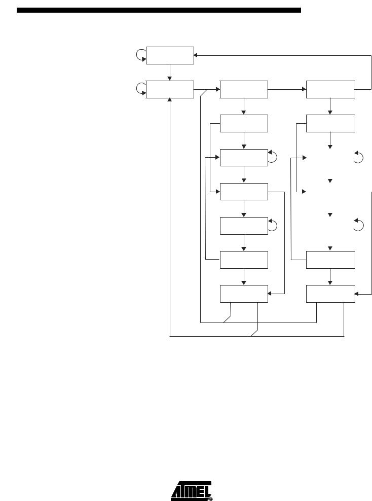
Programming Command The Programming Command Register is a 15-bit register. This register is used to seri- Register ally shift in programming commands, and to serially shift out the result of the previous command, if any. The JTAG Programming Instruction Set is shown in Table 117. The state sequence when shifting in the programming commands is illustrated in Figure 141.
275
2503F–AVR–12/03

ATmega32(L)
Table 117. JTAG Programming Instruction Set
a = address high bits, b = address low bits, H = 0 – Low byte, 1 – High Byte, o = data out, i = data in, x = don’t care
Instruction |
TDI sequence |
TDO sequence |
Notes |
|
|
|
|
|
|
1a. |
Chip erase |
0100011_10000000 |
xxxxxxx_xxxxxxxx |
|
|
|
0110001_10000000 |
xxxxxxx_xxxxxxxx |
|
|
|
0110011_10000000 |
xxxxxxx_xxxxxxxx |
|
|
|
0110011_10000000 |
xxxxxxx_xxxxxxxx |
|
|
|
|
|
|
1b. |
Poll for chip erase complete |
0110011_10000000 |
xxxxxox_xxxxxxxx |
(2) |
|
|
|
|
|
2a. |
Enter Flash Write |
0100011_00010000 |
xxxxxxx_xxxxxxxx |
|
|
|
|
|
|
2b. |
Load Address High Byte |
0000111_aaaaaaaa |
xxxxxxx_xxxxxxxx |
(9) |
|
|
|
|
|
2c. |
Load Address Low Byte |
0000011_bbbbbbbb |
xxxxxxx_xxxxxxxx |
|
|
|
|
|
|
2d. |
Load Data Low Byte |
0010011_iiiiiiii |
xxxxxxx_xxxxxxxx |
|
|
|
|
|
|
2e. |
Load Data High Byte |
0010111_iiiiiiii |
xxxxxxx_xxxxxxxx |
|
|
|
|
|
|
2f. Latch Data |
0110111_00000000 |
xxxxxxx_xxxxxxxx |
(1) |
|
|
|
1110111_00000000 |
xxxxxxx_xxxxxxxx |
|
|
|
0110111_00000000 |
xxxxxxx_xxxxxxxx |
|
|
|
|
|
|
2g. |
Write Flash Page |
0110111_00000000 |
xxxxxxx_xxxxxxxx |
(1) |
|
|
0110101_00000000 |
xxxxxxx_xxxxxxxx |
|
|
|
0110111_00000000 |
xxxxxxx_xxxxxxxx |
|
|
|
0110111_00000000 |
xxxxxxx_xxxxxxxx |
|
|
|
|
|
|
2h. |
Poll for Page Write complete |
0110111_00000000 |
xxxxxox_xxxxxxxx |
(2) |
|
|
|
|
|
3a. |
Enter Flash Read |
0100011_00000010 |
xxxxxxx_xxxxxxxx |
|
|
|
|
|
|
3b. |
Load Address High Byte |
0000111_aaaaaaaa |
xxxxxxx_xxxxxxxx |
(9) |
|
|
|
|
|
3c. |
Load Address Low Byte |
0000011_bbbbbbbb |
xxxxxxx_xxxxxxxx |
|
|
|
|
|
|
3d. Read Data Low and High Byte |
0110010_00000000 |
xxxxxxx_xxxxxxxx |
|
|
|
|
0110110_00000000 |
xxxxxxx_oooooooo |
low byte |
|
|
0110111_00000000 |
xxxxxxx_oooooooo |
high byte |
|
|
|
|
|
4a. Enter EEPROM Write |
0100011_00010001 |
xxxxxxx_xxxxxxxx |
|
|
|
|
|
|
|
4b. |
Load Address High Byte |
0000111_aaaaaaaa |
xxxxxxx_xxxxxxxx |
(9) |
|
|
|
|
|
4c. |
Load Address Low Byte |
0000011_bbbbbbbb |
xxxxxxx_xxxxxxxx |
|
|
|
|
|
|
4d. |
Load Data Byte |
0010011_iiiiiiii |
xxxxxxx_xxxxxxxx |
|
|
|
|
|
|
4e. |
Latch Data |
0110111_00000000 |
xxxxxxx_xxxxxxxx |
(1) |
|
|
1110111_00000000 |
xxxxxxx_xxxxxxxx |
|
|
|
0110111_00000000 |
xxxxxxx_xxxxxxxx |
|
|
|
|
|
|
4f. Write EEPROM Page |
0110011_00000000 |
xxxxxxx_xxxxxxxx |
(1) |
|
|
|
0110001_00000000 |
xxxxxxx_xxxxxxxx |
|
|
|
0110011_00000000 |
xxxxxxx_xxxxxxxx |
|
|
|
0110011_00000000 |
xxxxxxx_xxxxxxxx |
|
|
|
|
|
|
4g. |
Poll for Page Write complete |
0110011_00000000 |
xxxxxox_xxxxxxxx |
(2) |
|
|
|
|
|
5a. Enter EEPROM Read |
0100011_00000011 |
xxxxxxx_xxxxxxxx |
|
|
|
|
|
|
|
5b. |
Load Address High Byte |
0000111_aaaaaaaa |
xxxxxxx_xxxxxxxx |
(9) |
|
|
|
|
|
277
2503F–AVR–12/03

Table 117. JTAG Programming Instruction Set (Continued)
a = address high bits, b = address low bits, H = 0 – Low byte, 1 – High Byte, o = data out, i = data in, x = don’t care
Instruction |
TDI sequence |
TDO sequence |
Notes |
|
|
|
|
|
|
5c. Load Address Low Byte |
0000011_bbbbbbbb |
xxxxxxx_xxxxxxxx |
|
|
|
|
|
|
|
5d. |
Read Data Byte |
0110011_bbbbbbbb |
xxxxxxx_xxxxxxxx |
|
|
|
0110010_00000000 |
xxxxxxx_xxxxxxxx |
|
|
|
0110011_00000000 |
xxxxxxx_oooooooo |
|
|
|
|
|
|
6a. |
Enter Fuse Write |
0100011_01000000 |
xxxxxxx_xxxxxxxx |
|
|
|
|
|
|
6b. Load Data Low Byte(6) |
0010011_iiiiiiii |
xxxxxxx_xxxxxxxx |
(3) |
|
6c. Write Fuse High byte |
0110111_00000000 |
xxxxxxx_xxxxxxxx |
(1) |
|
|
|
0110101_00000000 |
xxxxxxx_xxxxxxxx |
|
|
|
0110111_00000000 |
xxxxxxx_xxxxxxxx |
|
|
|
0110111_00000000 |
xxxxxxx_xxxxxxxx |
|
|
|
|
|
|
6d. |
Poll for Fuse Write complete |
0110111_00000000 |
xxxxxox_xxxxxxxx |
(2) |
|
|
|
|
|
6e. |
Load Data Low Byte(7) |
0010011_iiiiiiii |
xxxxxxx_xxxxxxxx |
(3) |
6f. Write Fuse Low byte |
0110011_00000000 |
xxxxxxx_xxxxxxxx |
(1) |
|
|
|
0110001_00000000 |
xxxxxxx_xxxxxxxx |
|
|
|
0110011_00000000 |
xxxxxxx_xxxxxxxx |
|
|
|
0110011_00000000 |
xxxxxxx_xxxxxxxx |
|
|
|
|
|
|
6g. |
Poll for Fuse Write complete |
0110011_00000000 |
xxxxxox_xxxxxxxx |
(2) |
|
|
|
|
|
7a. |
Enter Lock Bit Write |
0100011_00100000 |
xxxxxxx_xxxxxxxx |
|
|
|
|
|
|
7b. Load Data Byte(8) |
0010011_11iiiiii |
xxxxxxx_xxxxxxxx |
(4) |
|
7c. Write Lock Bits |
0110011_00000000 |
xxxxxxx_xxxxxxxx |
(1) |
|
|
|
0110001_00000000 |
xxxxxxx_xxxxxxxx |
|
|
|
0110011_00000000 |
xxxxxxx_xxxxxxxx |
|
|
|
0110011_00000000 |
xxxxxxx_xxxxxxxx |
|
|
|
|
|
|
7d. |
Poll for Lock Bit Write complete |
0110011_00000000 |
xxxxxox_xxxxxxxx |
(2) |
|
|
|
|
|
8a. |
Enter Fuse/Lock Bit Read |
0100011_00000100 |
xxxxxxx_xxxxxxxx |
|
|
|
|
|
|
8b. Read Fuse High Byte(6) |
0111110_00000000 |
xxxxxxx_xxxxxxxx |
|
|
|
|
0111111_00000000 |
xxxxxxx_oooooooo |
|
|
|
|
|
|
8c. Read Fuse Low Byte(7) |
0110010_00000000 |
xxxxxxx_xxxxxxxx |
|
|
|
|
0110011_00000000 |
xxxxxxx_oooooooo |
|
|
|
|
|
|
8d. |
Read Lock Bits(8) |
0110110_00000000 |
xxxxxxx_xxxxxxxx |
(5) |
|
|
0110111_00000000 |
xxxxxxx_xxoooooo |
|
|
|
|
|
|
8e. |
Read Fuses and Lock Bits |
0111110_00000000 |
xxxxxxx_xxxxxxxx |
(5) |
|
|
0110010_00000000 |
xxxxxxx_oooooooo |
fuse high byte |
|
|
0110110_00000000 |
xxxxxxx_oooooooo |
fuse low byte |
|
|
0110111_00000000 |
xxxxxxx_oooooooo |
lock bits |
|
|
|
|
|
9a. |
Enter Signature Byte Read |
0100011_00001000 |
xxxxxxx_xxxxxxxx |
|
|
|
|
|
|
9b. Load Address Byte |
0000011_bbbbbbbb |
xxxxxxx_xxxxxxxx |
|
|
|
|
|
|
|
9c. Read Signature Byte |
0110010_00000000 |
xxxxxxx_xxxxxxxx |
|
|
|
|
0110011_00000000 |
xxxxxxx_oooooooo |
|
|
|
|
|
|
278 ATmega32(L)
2503F–AVR–12/03

 ATmega32(L)
Table 117. JTAG Programming Instruction Set (Continued)
a = address high bits, b = address low bits, H = 0 – Low byte, 1 – High Byte, o = data out, i = data in, x = don’t care
Instruction |
TDI sequence |
TDO sequence |
Notes |
|
|
|
|
10a. Enter Calibration Byte Read |
0100011_00001000 |
xxxxxxx_xxxxxxxx |
|
|
|
|
|
10b. Load Address Byte |
0000011_bbbbbbbb |
xxxxxxx_xxxxxxxx |
|
|
|
|
|
10c. Read Calibration Byte |
0110110_00000000 |
xxxxxxx_xxxxxxxx |
|
|
0110111_00000000 |
xxxxxxx_oooooooo |
|
|
|
|
|
11a. Load No Operation Command |
0100011_00000000 |
xxxxxxx_xxxxxxxx |
|
|
0110011_00000000 |
xxxxxxx_xxxxxxxx |
|
|
|
|
|
Notes: 1. This command sequence is not required if the seven MSB are correctly set by the previous command sequence (which is normally the case).
2.Repeat until o = “1”.
3.Set bits to “0” to program the corresponding fuse, “1” to unprogram the fuse.
4.Set bits to “0” to program the corresponding lock bit, “1” to leave the lock bit unchanged.
5.“0” = programmed, “1” = unprogrammed.
6.The bit mapping for fuses high byte is listed in Table 105 on page 255
7.The bit mapping for fuses low byte is listed in Table 106 on page 256
8.The bit mapping for Lock bits byte is listed in Table 103 on page 254
9.Address bits exceeding PCMSB and EEAMSB (Table 111 and Table 112) are don’t care
279
2503F–AVR–12/03