- •Features
- •Pin Configurations
- •Disclaimer
- •Overview
- •Block Diagram
- •Pin Descriptions
- •Port A (PA7..PA0)
- •Port B (PB7..PB0)
- •Port C (PC7..PC0)
- •Port D (PD7..PD0)
- •RESET
- •XTAL1
- •XTAL2
- •AVCC
- •AREF
- •AVR CPU Core
- •Introduction
- •Architectural Overview
- •Status Register
- •Stack Pointer
- •Interrupt Response Time
- •SRAM Data Memory
- •Data Memory Access Times
- •EEPROM Data Memory
- •EEPROM Read/Write Access
- •I/O Memory
- •Clock Systems and their Distribution
- •CPU Clock – clkCPU
- •I/O Clock – clkI/O
- •Flash Clock – clkFLASH
- •ADC Clock – clkADC
- •Clock Sources
- •Default Clock Source
- •Crystal Oscillator
- •External RC Oscillator
- •External Clock
- •Timer/Counter Oscillator
- •Idle Mode
- •Power-down Mode
- •Power-save Mode
- •Standby Mode
- •Extended Standby Mode
- •Analog to Digital Converter
- •Analog Comparator
- •Brown-out Detector
- •Internal Voltage Reference
- •Watchdog Timer
- •Port Pins
- •Resetting the AVR
- •Reset Sources
- •Power-on Reset
- •External Reset
- •Brown-out Detection
- •Watchdog Reset
- •Watchdog Timer
- •Interrupts
- •I/O Ports
- •Introduction
- •Configuring the Pin
- •Reading the Pin Value
- •Unconnected pins
- •Alternate Port Functions
- •Alternate Functions of Port A
- •Alternate Functions of Port B
- •Alternate Functions of Port C
- •Alternate Functions of Port D
- •Port A Data Register – PORTA
- •Port B Data Register – PORTB
- •Port C Data Register – PORTC
- •Port D Data Register – PORTD
- •External Interrupts
- •8-bit Timer/Counter0 with PWM
- •Overview
- •Registers
- •Definitions
- •Counter Unit
- •Output Compare Unit
- •Force Output Compare
- •Modes of Operation
- •Normal Mode
- •Fast PWM Mode
- •Phase Correct PWM Mode
- •Internal Clock Source
- •Prescaler Reset
- •External Clock Source
- •16-bit Timer/Counter1
- •Overview
- •Registers
- •Definitions
- •Compatibility
- •Counter Unit
- •Input Capture Unit
- •Input Capture Trigger Source
- •Noise Canceler
- •Using the Input Capture Unit
- •Output Compare Units
- •Force Output Compare
- •Modes of Operation
- •Normal Mode
- •Fast PWM Mode
- •Phase Correct PWM Mode
- •8-bit Timer/Counter2 with PWM and Asynchronous Operation
- •Overview
- •Registers
- •Definitions
- •Counter Unit
- •Output Compare Unit
- •Force Output Compare
- •Modes of Operation
- •Normal Mode
- •Fast PWM Mode
- •Phase Correct PWM Mode
- •Timer/Counter Prescaler
- •SS Pin Functionality
- •Slave Mode
- •Master Mode
- •SPI Control Register – SPCR
- •SPI Status Register – SPSR
- •SPI Data Register – SPDR
- •Data Modes
- •USART
- •Overview
- •AVR USART vs. AVR UART – Compatibility
- •Clock Generation
- •External Clock
- •Synchronous Clock Operation
- •Frame Formats
- •Parity Bit Calculation
- •USART Initialization
- •Parity Generator
- •Disabling the Transmitter
- •Receiver Error Flags
- •Parity Checker
- •Disabling the Receiver
- •Flushing the Receive Buffer
- •Asynchronous Data Recovery
- •Using MPCM
- •Write Access
- •Read Access
- •Two-wire Serial Interface
- •Features
- •TWI Terminology
- •Electrical Interconnection
- •Transferring Bits
- •START and STOP Conditions
- •Address Packet Format
- •Data Packet Format
- •Overview of the TWI Module
- •SCL and SDA Pins
- •Bit Rate Generator Unit
- •Bus Interface Unit
- •Address Match Unit
- •Control Unit
- •TWI Register Description
- •TWI Bit Rate Register – TWBR
- •TWI Control Register – TWCR
- •TWI Status Register – TWSR
- •TWI Data Register – TWDR
- •Using the TWI
- •Transmission Modes
- •Master Transmitter Mode
- •Master Receiver Mode
- •Slave Receiver Mode
- •Slave Transmitter Mode
- •Miscellaneous States
- •Analog Comparator
- •Analog Comparator Multiplexed Input
- •Features
- •Operation
- •Starting a Conversion
- •Differential Gain Channels
- •Changing Channel or Reference Selection
- •ADC Input Channels
- •ADC Voltage Reference
- •ADC Noise Canceler
- •Analog Input Circuitry
- •ADC Accuracy Definitions
- •ADC Conversion Result
- •ADLAR = 0
- •ADLAR = 1
- •Features
- •Overview
- •Test Access Port – TAP
- •TAP Controller
- •PRIVATE0; $8
- •PRIVATE1; $9
- •PRIVATE2; $A
- •PRIVATE3; $B
- •Bibliography
- •Features
- •System Overview
- •Data Registers
- •Bypass Register
- •Device Identification Register
- •Reset Register
- •Boundary-scan Chain
- •EXTEST; $0
- •IDCODE; $1
- •SAMPLE_PRELOAD; $2
- •AVR_RESET; $C
- •BYPASS; $F
- •Scanning the Digital Port Pins
- •Scanning the RESET Pin
- •Scanning the Clock Pins
- •Scanning the ADC
- •Features
- •Application Section
- •BLS – Boot Loader Section
- •Read-While-Write and no Read-While-Write Flash Sections
- •Boot Loader Lock Bits
- •Performing a Page Write
- •Using the SPM Interrupt
- •Setting the Boot Loader Lock Bits by SPM
- •Reading the Fuse and Lock Bits from Software
- •Preventing Flash Corruption
- •Fuse Bits
- •Latching of Fuses
- •Signature Bytes
- •Calibration Byte
- •Signal Names
- •Parallel Programming
- •Enter Programming Mode
- •Chip Erase
- •Programming the Flash
- •Programming the EEPROM
- •Reading the Flash
- •Reading the EEPROM
- •Programming the Lock Bits
- •Reading the Signature Bytes
- •Reading the Calibration Byte
- •SPI Serial Downloading
- •Data Polling Flash
- •Data Polling EEPROM
- •AVR_RESET ($C)
- •PROG_ENABLE ($4)
- •PROG_COMMANDS ($5)
- •PROG_PAGELOAD ($6)
- •PROG_PAGEREAD ($7)
- •Data Registers
- •Reset Register
- •Programming Enable Register
- •Virtual Flash Page Read Register
- •Programming Algorithm
- •Entering Programming Mode
- •Leaving Programming Mode
- •Performing Chip Erase
- •Programming the Flash
- •Reading the Flash
- •Programming the EEPROM
- •Reading the EEPROM
- •Programming the Fuses
- •Programming the Lock Bits
- •Reading the Signature Bytes
- •Reading the Calibration Byte
- •Electrical Characteristics
- •Absolute Maximum Ratings*
- •DC Characteristics
- •External Clock Drive Waveforms
- •External Clock Drive
- •Two-wire Serial Interface Characteristics
- •ADC Characteristics
- •Register Summary
- •Instruction Set Summary
- •Ordering Information
- •Packaging Information
- •Errata
- •ATmega32 Rev. A
- •Datasheet Change Log for ATmega32
- •Changes from Rev. 2503E-09/03 to Rev. 2503F-12/03
- •Changes from Rev. 2503D-02/03 to Rev. 2503E-09/03
- •Changes from Rev. 2503C-10/02 to Rev. 2503D-02/03
- •Changes from Rev. 2503B-10/02 to Rev. 2503C-10/02
- •Changes from Rev. 2503A-03/02 to Rev. 2503B-10/02
- •Table of Contents
ATmega32(L)
The following code examples show how to do an atomic write of the TCNT1 Register contents. Writing any of the OCR1A/B or ICR1 Registers can be done by using the same principle.
Assembly Code Example(1) |
||
|
|
|
|
TIM16_WriteTCNT1: |
|
|
; Save global interrupt flag |
|
|
in |
r18,SREG |
|
; Disable interrupts |
|
|
cli |
|
|
; Set TCNT1 to r17:r16 |
|
|
out TCNT1H,r17 |
|
|
out TCNT1L,r16 |
|
|
; Restore global interrupt flag |
|
|
out SREG,r18 |
|
|
ret |
|
|
||
C Code Example(1) |
||
|
|
|
|
void TIM16_WriteTCNT1 ( unsigned int i ) |
|
|
{ |
|
|
unsigned char sreg; |
|
|
unsigned int i; |
|
|
/* Save global interrupt flag */ |
|
|
sreg = SREG; |
|
|
/* Disable interrupts */ |
|
|
_CLI(); |
|
|
/* Set TCNT1 to i */ |
|
|
TCNT1 = i; |
|
|
/* Restore global interrupt flag */ |
|
|
SREG = sreg; |
|
|
} |
|
|
|
|
Note: |
1. |
The example code assumes that the part specific header file is included. |
The assembly code example requires that the r17:r16 register pair contains the value to be written to TCNT1.
Reusing the Temporary High |
If writing to more than one 16-bit register where the high byte is the same for all registers |
Byte Register |
written, then the high byte only needs to be written once. However, note that the same |
|
rule of atomic operation described previously also applies in this case. |
Timer/Counter Clock |
The Timer/Counter can be clocked by an internal or an external clock source. The clock |
Sources |
source is selected by the Clock Select logic which is controlled by the Clock Select |
|
(CS12:0) bits located in the Timer/Counter Control Register B (TCCR1B). For details on |
|
clock sources and prescaler, see “Timer/Counter0 and Timer/Counter1 Prescalers” on |
|
page 82. |
Counter Unit |
The main part of the 16-bit Timer/Counter is the programmable 16-bit bi-directional |
|
counter unit. Figure 41 shows a block diagram of the counter and its surroundings. |
89
2503F–AVR–12/03
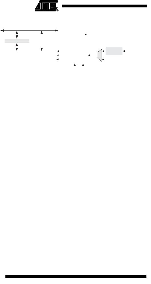
Figure 41. Counter Unit Block Diagram
DATA BUS (8-bit)
|
|
|
|
|
|
|
|
|
|
|
|
|
|
|
TOVn |
|
|
|
|
|
|
|
||||
|
|
|
|
|
|
|
|
|
|
|
|
|
|
|
(Int.Req.) |
|
|
|
|
|
|
|
||||
|
|
|
|
|
|
|
|
|
|
|
|
|
|
|
|
|
|
|
|
|
|
|
|
|
|
|
|
TEMP (8-bit) |
|
|
|
|
|
|
|
|
|
|
|
|
|
|
|
|
|
|
|
|
|
|
|
||
|
|
|
|
|
|
|
|
|
|
|
|
|
|
|
|
|
|
|
|
|
|
|
|
|
|
|
|
|
|
|
|
|
|
|
|
|
|
|
|
|
|
|
|
|
|
|
Clock Select |
|
|
||||
|
|
|
|
|
|
|
|
|
Count |
|
|
|
|
|
|
|
|
|
|
Edge |
|
|
|
|
Tn |
|
|
TCNTnH (8-bit) |
TCNTnL (8-bit) |
|
|
|
Clear |
Control Logic |
clkTn |
|
|
|
Detector |
|
|
|
|
||||||||||
|
|
TCNTn (16-bit Counter) |
|
|
|
Direction |
|
|
|
|
|
|
|
|
|
|
|
|
||||||||
|
|
|
|
|
|
|
|
|
|
|
|
|
|
|
|
|
|
|
|
|
||||||
|
|
|
|
|
|
|
|
|
|
|
|
|
|
|
|
|
|
|
|
|
|
|||||
|
|
|
|
|
|
|
|
|
|
|
|
|
|
|
|
|
|
|
|
|
|
|
|
|
|
|
|
|
|
|
|
|
|
|
|
|
|
|
|
|
|
|
|
|
|
|
( From Prescaler ) |
|
|
|
|||
|
|
|
|
|
|
|
|
|
|
|
|
|
|
|
|
|
|
|
|
|
|
|||||
|
|
|
|
|
|
|
|
|
|
|
|
|
|
|
|
|
|
|
|
|
|
|
|
|
|
|
|
|
|
|
|
|
|
|
|
|
|
|
|
|
|
|
|
|
|
|
|
|
|
|
|
|
|
|
|
|
|
|
|
|
|
|
|
|
TOP |
BOTTOM |
|
|
|
|
|
|
|
|||||||
|
|
|
|
|
|
|
|
|
|
|
|
|
|
|
|
|
|
|
|
|
|
|
|
|
|
|
Signal description (internal signals):
Count |
Increment or decrement TCNT1 by 1. |
Direction |
Select between increment and decrement. |
Clear |
Clear TCNT1 (set all bits to zero). |
clkT1 |
Timer/Counter clock. |
TOP |
Signalize that TCNT1 has reached maximum value. |
BOTTOM |
Signalize that TCNT1 has reached minimum value (zero). |
The 16-bit counter is mapped into two 8-bit I/O memory locations: Counter High (TCNT1H) containing the upper eight bits of the counter, and Counter Low (TCNT1L) containing the lower 8 bits. The TCNT1H Register can only be indirectly accessed by the CPU. When the CPU does an access to the TCNT1H I/O location, the CPU accesses the high byte temporary register (TEMP). The temporary register is updated with the TCNT1H value when the TCNT1L is read, and TCNT1H is updated with the temporary register value when TCNT1L is written. This allows the CPU to read or write the entire 16-bit counter value within one clock cycle via the 8-bit data bus. It is important to notice that there are special cases of writing to the TCNT1 Register when the counter is counting that will give unpredictable results. The special cases are described in the sections where they are of importance.
Depending on the mode of operation used, the counter is cleared, incremented, or decremented at each timer clock (clkT1). The clkT1 can be generated from an external or internal clock source, selected by the Clock Select bits (CS12:0). When no clock source is selected (CS12:0 = 0) the timer is stopped. However, the TCNT1 value can be accessed by the CPU, independent of whether clkT1 is present or not. A CPU write overrides (has priority over) all counter clear or count operations.
The counting sequence is determined by the setting of the Waveform Generation Mode bits (WGM13:0) located in the Timer/Counter Control Registers A and B (TCCR1A and TCCR1B). There are close connections between how the counter behaves (counts) and how waveforms are generated on the Output Compare outputs OC1x. For more details about advanced counting sequences and waveform generation, see “Modes of Operation” on page 95.
The Timer/Counter Overflow (TOV1) Flag is set according to the mode of operation selected by the WGM13:0 bits. TOV1 can be used for generating a CPU interrupt.
90 ATmega32(L)
2503F–AVR–12/03