


AVR USART vs. AVR UART – Compatibility
Clock Generation
2503F–AVR–12/03
ATmega32(L)
The dashed boxes in the block diagram separate the three main parts of the USART (listed from the top): Clock Generator, Transmitter and Receiver. Control Registers are shared by all units. The clock generation logic consists of synchronization logic for external clock input used by synchronous slave operation, and the baud rate generator. The XCK (Transfer Clock) pin is only used by Synchronous Transfer mode. The Transmitter consists of a single write buffer, a serial Shift Register, parity generator and control logic for handling different serial frame formats. The write buffer allows a continuous transfer of data without any delay between frames. The Receiver is the most complex part of the USART module due to its clock and data recovery units. The recovery units are used for asynchronous data reception. In addition to the recovery units, the receiver includes a parity checker, control logic, a Shift Register and a two level receive buffer (UDR). The receiver supports the same frame formats as the transmitter, and can detect frame error, data overrun and parity errors.
The USART is fully compatible with the AVR UART regarding:
•Bit locations inside all USART Registers
•Baud Rate Generation
•Transmitter Operation
•Transmit Buffer Functionality
•Receiver Operation
However, the receive buffering has two improvements that will affect the compatibility in some special cases:
•A second Buffer Register has been added. The two Buffer Registers operate as a circular FIFO buffer. Therefore the UDR must only be read once for each incoming data! More important is the fact that the Error Flags (FE and DOR) and the 9th data bit (RXB8) are buffered with the data in the receive buffer. Therefore the status bits must always be read before the UDR Register is read. Otherwise the error status will be lost since the buffer state is lost.
•The receiver Shift Register can now act as a third buffer level. This is done by allowing the received data to remain in the serial Shift Register (see Figure 69) if the Buffer Registers are full, until a new start bit is detected. The USART is therefore more resistant to Data OverRun (DOR) error conditions.
The following control bits have changed name, but have same functionality and register location:
•CHR9 is changed to UCSZ2
•OR is changed to DOR
The clock generation logic generates the base clock for the Transmitter and Receiver. The USART supports four modes of clock operation: Normal Asynchronous, Double Speed Asynchronous, Master Synchronous and Slave Synchronous mode. The UMSEL bit in USART Control and Status Register C (UCSRC) selects between asynchronous and synchronous operation. Double Speed (Asynchronous mode only) is controlled by the U2X found in the UCSRA Register. When using Synchronous mode (UMSEL = 1), the Data Direction Register for the XCK pin (DDR_XCK) controls whether the clock source is internal (Master mode) or external (Slave mode). The XCK pin is only active when using Synchronous mode.
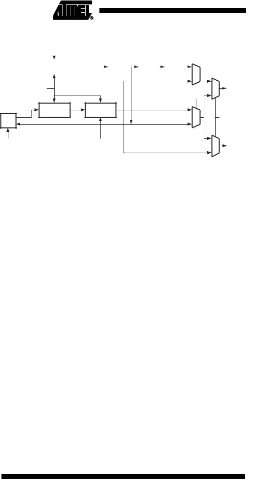
Figure 70 shows a block diagram of the clock generation logic.
139
Internal Clock Generation –
The Baud Rate Generator
Figure 70. Clock Generation Logic, Block Diagram
UBRR |
|
|
|
|
|
|
|
|
|
|
|
|
|
U2X |
|
|||
|
|
|
fosc |
|
|
|
|
|
|
|
|
|
||||||
|
|
|
|
|
|
|
||||||||||||
|
|
|
|
|
|
|
|
|
|
|
|
|
|
|
||||
|
|
|
|
|
|
|
|
|
|
|
|
|
|
|
|
|
|
|
Prescaling |
|
UBRR+1 |
/ 2 |
|
|
/ 4 |
|
|
|
/ 2 |
|
|
|
|
|
|||
|
|
|
|
|
|
|
|
|
|
|
|
|
|
|||||
Down-Counter |
|
|
|
|
|
|
|
|
|
|
|
|
0 |
|
|
|||
|
|
|
|
|
|
|
|
|
|
|
|
|
|
|
|
|||
|
|
|
|
|
|
|
|
|
|
|
|
|
|
|
|
|
|
|
|
|
|
|
|
|
|
|
|
|
|
1 |
|
|
|||||
|
|
|
|
|
|
|
|
|
|
|
|
|
|
|
|
|
|
|
|
|
OSC |
|
0 |
|
|
|
txclk |
|
|
|
|
|
1 |
|
|
|
|
DDR_XCK |
|
|
Sync |
Edge |
|
|
xcki |
Register |
Detector |
0 |
XCK |
|
|
|
UMSEL |
xcko |
|
|
1 |
|
Pin |
|
|
||
|
|
|
|
DDR_XCK |
UCPOL |
1 |
|
rxclk |
|
|
0 |
|
|
|
|
|
|
Signal description:
txclk Transmitter clock (Internal Signal). rxclk Receiver base clock (Internal Signal).
xcki Input from XCK pin (Internal Signal). Used for synchronous slave operation.
xcko Clock output to XCK pin (Internal Signal). Used for synchronous master operation.
fosc XTAL pin frequency (System Clock).
Internal clock generation is used for the asynchronous and the synchronous master modes of operation. The description in this section refers to Figure 70.
The USART Baud Rate Register (UBRR) and the down-counter connected to it function as a programmable prescaler or baud rate generator. The down-counter, running at system clock (fosc), is loaded with the UBRR value each time the counter has counted down to zero or when the UBRRL Register is written. A clock is generated each time the counter reaches zero. This clock is the baud rate generator clock output (= fosc/(UBRR+1)). The Transmitter divides the baud rate generator clock output by 2, 8 or 16 depending on mode. The baud rate generator output is used directly by the receiver’s clock and data recovery units. However, the recovery units use a state machine that uses 2, 8 or 16 states depending on mode set by the state of the UMSEL, U2X and DDR_XCK bits.
Table 60 contains equations for calculating the baud rate (in bits per second) and for calculating the UBRR value for each mode of operation using an internally generated clock source.
140 ATmega32(L)
2503F–AVR–12/03
|
|
|
|
|
|
|
|
ATmega32(L) |
|||
|
|
|
|
|
|
|
|
||||
|
|
|
|
|
|
|
|
||||
|
|
Table 60. Equations for Calculating Baud Rate Register Setting |
|
|
|||||||
|
|
|
|
||||||||
|
|
|
|
|
|
|
|
|
|
|
|
|
|
|
|
|
|
|
|
|
|
Equation for |
|
|
|
|
|
Equation for Calculating |
|
Calculating UBRR |
|||||
|
|
Operating Mode |
|
|
Baud Rate(1) |
|
Value |
|
|||
|
|
Asynchronous Normal Mode |
|
|
|
fOS C |
|
fO SC |
– 1 |
||
|
|
(U2X = 0) |
|
BAUD = |
|
||||||
|
|
|
----------------------------- |
--- |
|
UBRR = ----------------------- |
|||||
|
|
|
|
|
|
16(UBRR + 1) |
|
16BAUD |
|
||
|
|
Asynchronous Double Speed Mode |
|
|
|
fOS C |
|
fOS C |
– 1 |
||
|
|
(U2X = 1) |
|
BAUD = |
|
||||||
|
|
|
-----------------------------(UBRR + 1--) |
|
UBRR = -------------------- |
||||||
|
|
|
|
|
|
8 |
|
8BAUD |
|
||
|
|
Synchronous Master Mode |
|
|
|
fOS C |
|
fOS C |
– 1 |
||
|
|
|
|
BAUD = |
|
||||||
|
|
|
|
-----------------------------(UBRR + 1--) |
|
UBRR = -------------------- |
|||||
|
|
|
|
|
|
2 |
|
2BAUD |
|
||
|
|
Note: 1. |
The baud rate is defined to be the transfer rate in bit per second (bps). |
|
|||||||
|
|
BAUD |
Baud rate (in bits per second, bps) |
|
|
|
|
|
|||
|
|
fOSC |
System Oscillator clock frequency |
|
|
|
|
|
|||
|
|
UBRR |
Contents of the UBRRH and UBRRL Registers, (0 - 4095) |
|
|||||||
|
|
Some examples of UBRR values for some system clock frequencies are found in Table |
|||||||||
|
|
68 (see page 163). |
|
|
|
|
|
|
|
||
|
Double Speed Operation |
The transfer rate can be doubled by setting the U2X bit in UCSRA. Setting this bit only |
|||||||||
|
(U2X) |
has effect for the asynchronous operation. Set this bit to zero when using synchronous |
|||||||||
|
|
operation. |
|
|
|
|
|
|
|
|
|
|
|
Setting this bit will reduce the divisor of the baud rate divider from 16 to 8, effectively |
|||||||||
|
|
doubling the transfer rate for asynchronous communication. Note however that the |
|||||||||
|
|
receiver will in this case only use half the number of samples (reduced from 16 to 8) for |
|||||||||
|
|
data sampling and clock recovery, and therefore a more accurate baud rate setting and |
|||||||||
|
|
system clock are required when this mode is used. For the Transmitter, there are no |
|||||||||
|
|
downsides. |
|
|
|
|
|
|
|
||
|
External Clock |
External clocking is used by the synchronous slave modes of operation. The description |
|||||||||
|
|
in this section refers to Figure 70 for details. |
|
|
|
|
|
||||
|
|
External clock input from the XCK pin is sampled by a synchronization register to mini- |
|||||||||
|
|
mize the chance of meta-stability. The output from the synchronization register must |
|||||||||
|
|
then pass through an edge detector before it can be used by the Transmitter and |
|||||||||
|
|
receiver. This process introduces a two CPU clock period delay and therefore the maxi- |
|||||||||
|
|
mum external XCK clock frequency is limited by the following equation: |
|
||||||||
|
|
|
|
f |
|
fOS C |
|
|
|
|
|
|
|
|
|
XCK |
< ---------- |
|
|
|
|
|
|
|
|
|
|
|
4 |
|
|
|
|
|
|
Note that fosc depends on the stability of the system clock source. It is therefore recommended to add some margin to avoid possible loss of data due to frequency variations.
Synchronous Clock Operation When Synchronous mode is used (UMSEL = 1), the XCK pin will be used as either clock input (Slave) or clock output (Master). The dependency between the clock edges and data sampling or data change is the same. The basic principle is that data input (on RxD) is sampled at the opposite XCK clock edge of the edge the data output (TxD) is changed.
141
2503F–AVR–12/03