- •Features
- •Pin Configurations
- •Disclaimer
- •Overview
- •Block Diagram
- •Pin Descriptions
- •Port A (PA7..PA0)
- •Port B (PB7..PB0)
- •Port C (PC7..PC0)
- •Port D (PD7..PD0)
- •RESET
- •XTAL1
- •XTAL2
- •AVCC
- •AREF
- •AVR CPU Core
- •Introduction
- •Architectural Overview
- •Status Register
- •Stack Pointer
- •Interrupt Response Time
- •SRAM Data Memory
- •Data Memory Access Times
- •EEPROM Data Memory
- •EEPROM Read/Write Access
- •I/O Memory
- •Clock Systems and their Distribution
- •CPU Clock – clkCPU
- •I/O Clock – clkI/O
- •Flash Clock – clkFLASH
- •ADC Clock – clkADC
- •Clock Sources
- •Default Clock Source
- •Crystal Oscillator
- •External RC Oscillator
- •External Clock
- •Timer/Counter Oscillator
- •Idle Mode
- •Power-down Mode
- •Power-save Mode
- •Standby Mode
- •Extended Standby Mode
- •Analog to Digital Converter
- •Analog Comparator
- •Brown-out Detector
- •Internal Voltage Reference
- •Watchdog Timer
- •Port Pins
- •Resetting the AVR
- •Reset Sources
- •Power-on Reset
- •External Reset
- •Brown-out Detection
- •Watchdog Reset
- •Watchdog Timer
- •Interrupts
- •I/O Ports
- •Introduction
- •Configuring the Pin
- •Reading the Pin Value
- •Unconnected pins
- •Alternate Port Functions
- •Alternate Functions of Port A
- •Alternate Functions of Port B
- •Alternate Functions of Port C
- •Alternate Functions of Port D
- •Port A Data Register – PORTA
- •Port B Data Register – PORTB
- •Port C Data Register – PORTC
- •Port D Data Register – PORTD
- •External Interrupts
- •8-bit Timer/Counter0 with PWM
- •Overview
- •Registers
- •Definitions
- •Counter Unit
- •Output Compare Unit
- •Force Output Compare
- •Modes of Operation
- •Normal Mode
- •Fast PWM Mode
- •Phase Correct PWM Mode
- •Internal Clock Source
- •Prescaler Reset
- •External Clock Source
- •16-bit Timer/Counter1
- •Overview
- •Registers
- •Definitions
- •Compatibility
- •Counter Unit
- •Input Capture Unit
- •Input Capture Trigger Source
- •Noise Canceler
- •Using the Input Capture Unit
- •Output Compare Units
- •Force Output Compare
- •Modes of Operation
- •Normal Mode
- •Fast PWM Mode
- •Phase Correct PWM Mode
- •8-bit Timer/Counter2 with PWM and Asynchronous Operation
- •Overview
- •Registers
- •Definitions
- •Counter Unit
- •Output Compare Unit
- •Force Output Compare
- •Modes of Operation
- •Normal Mode
- •Fast PWM Mode
- •Phase Correct PWM Mode
- •Timer/Counter Prescaler
- •SS Pin Functionality
- •Slave Mode
- •Master Mode
- •SPI Control Register – SPCR
- •SPI Status Register – SPSR
- •SPI Data Register – SPDR
- •Data Modes
- •USART
- •Overview
- •AVR USART vs. AVR UART – Compatibility
- •Clock Generation
- •External Clock
- •Synchronous Clock Operation
- •Frame Formats
- •Parity Bit Calculation
- •USART Initialization
- •Parity Generator
- •Disabling the Transmitter
- •Receiver Error Flags
- •Parity Checker
- •Disabling the Receiver
- •Flushing the Receive Buffer
- •Asynchronous Data Recovery
- •Using MPCM
- •Write Access
- •Read Access
- •Two-wire Serial Interface
- •Features
- •TWI Terminology
- •Electrical Interconnection
- •Transferring Bits
- •START and STOP Conditions
- •Address Packet Format
- •Data Packet Format
- •Overview of the TWI Module
- •SCL and SDA Pins
- •Bit Rate Generator Unit
- •Bus Interface Unit
- •Address Match Unit
- •Control Unit
- •TWI Register Description
- •TWI Bit Rate Register – TWBR
- •TWI Control Register – TWCR
- •TWI Status Register – TWSR
- •TWI Data Register – TWDR
- •Using the TWI
- •Transmission Modes
- •Master Transmitter Mode
- •Master Receiver Mode
- •Slave Receiver Mode
- •Slave Transmitter Mode
- •Miscellaneous States
- •Analog Comparator
- •Analog Comparator Multiplexed Input
- •Features
- •Operation
- •Starting a Conversion
- •Differential Gain Channels
- •Changing Channel or Reference Selection
- •ADC Input Channels
- •ADC Voltage Reference
- •ADC Noise Canceler
- •Analog Input Circuitry
- •ADC Accuracy Definitions
- •ADC Conversion Result
- •ADLAR = 0
- •ADLAR = 1
- •Features
- •Overview
- •Test Access Port – TAP
- •TAP Controller
- •PRIVATE0; $8
- •PRIVATE1; $9
- •PRIVATE2; $A
- •PRIVATE3; $B
- •Bibliography
- •Features
- •System Overview
- •Data Registers
- •Bypass Register
- •Device Identification Register
- •Reset Register
- •Boundary-scan Chain
- •EXTEST; $0
- •IDCODE; $1
- •SAMPLE_PRELOAD; $2
- •AVR_RESET; $C
- •BYPASS; $F
- •Scanning the Digital Port Pins
- •Scanning the RESET Pin
- •Scanning the Clock Pins
- •Scanning the ADC
- •Features
- •Application Section
- •BLS – Boot Loader Section
- •Read-While-Write and no Read-While-Write Flash Sections
- •Boot Loader Lock Bits
- •Performing a Page Write
- •Using the SPM Interrupt
- •Setting the Boot Loader Lock Bits by SPM
- •Reading the Fuse and Lock Bits from Software
- •Preventing Flash Corruption
- •Fuse Bits
- •Latching of Fuses
- •Signature Bytes
- •Calibration Byte
- •Signal Names
- •Parallel Programming
- •Enter Programming Mode
- •Chip Erase
- •Programming the Flash
- •Programming the EEPROM
- •Reading the Flash
- •Reading the EEPROM
- •Programming the Lock Bits
- •Reading the Signature Bytes
- •Reading the Calibration Byte
- •SPI Serial Downloading
- •Data Polling Flash
- •Data Polling EEPROM
- •AVR_RESET ($C)
- •PROG_ENABLE ($4)
- •PROG_COMMANDS ($5)
- •PROG_PAGELOAD ($6)
- •PROG_PAGEREAD ($7)
- •Data Registers
- •Reset Register
- •Programming Enable Register
- •Virtual Flash Page Read Register
- •Programming Algorithm
- •Entering Programming Mode
- •Leaving Programming Mode
- •Performing Chip Erase
- •Programming the Flash
- •Reading the Flash
- •Programming the EEPROM
- •Reading the EEPROM
- •Programming the Fuses
- •Programming the Lock Bits
- •Reading the Signature Bytes
- •Reading the Calibration Byte
- •Electrical Characteristics
- •Absolute Maximum Ratings*
- •DC Characteristics
- •External Clock Drive Waveforms
- •External Clock Drive
- •Two-wire Serial Interface Characteristics
- •ADC Characteristics
- •Register Summary
- •Instruction Set Summary
- •Ordering Information
- •Packaging Information
- •Errata
- •ATmega32 Rev. A
- •Datasheet Change Log for ATmega32
- •Changes from Rev. 2503E-09/03 to Rev. 2503F-12/03
- •Changes from Rev. 2503D-02/03 to Rev. 2503E-09/03
- •Changes from Rev. 2503C-10/02 to Rev. 2503D-02/03
- •Changes from Rev. 2503B-10/02 to Rev. 2503C-10/02
- •Changes from Rev. 2503A-03/02 to Rev. 2503B-10/02
- •Table of Contents
ATmega32(L)
ADC Characteristics
Table 122. |
ADC Characteristics, Single Ended channels, TA = -40°C to 85°C |
|
|
|
|
||
Symbol |
|
Parameter |
Condition |
Min |
Typ |
Max |
Units |
|
|
|
|
|
|
|
|
|
|
Resolution |
Single Ended Conversion |
|
10 |
|
Bits |
|
|
|
|
|
|
|
|
|
|
|
Single Ended Conversion |
|
|
|
|
|
|
|
VREF = 4V, VCC = 4V |
|
1.5 |
|
LSB |
|
|
|
ADC clock = 200 kHz |
|
|
|
|
|
|
|
|
|
|
|
|
|
|
|
Single Ended Conversion |
|
|
|
|
|
|
|
VREF = 4V, VCC = 4V |
|
3 |
|
LSB |
|
|
|
ADC clock = 1 MHz |
|
|
|
|
|
|
Absolute Accuracy (Including INL, DNL, |
|
|
|
|
|
|
|
Single Ended Conversion |
|
|
|
|
|
|
|
Quantization Error, Gain, and Offset Error) |
|
|
|
|
|
|
|
VREF = 4V, VCC = 4V |
|
1.5 |
|
LSB |
|
|
|
|
|
|
|||
|
|
|
ADC clock = 200 kHz |
|
|
||
|
|
|
|
|
|
|
|
|
|
|
Noise Reduction mode |
|
|
|
|
|
|
|
|
|
|
|
|
|
|
|
Single Ended Conversion |
|
|
|
|
|
|
|
VREF = 4V, VCC = 4V |
|
3 |
|
LSB |
|
|
|
ADC clock = 1 MHz |
|
|
||
|
|
|
|
|
|
|
|
|
|
|
Noise Reduction mode |
|
|
|
|
|
|
|
|
|
|
|
|
|
|
|
Single Ended Conversion |
|
|
|
|
|
|
Integral Non-Linearity (INL) |
VREF = 4V, VCC = 4V |
|
0.75 |
|
LSB |
|
|
|
ADC clock = 200 kHz |
|
|
|
|
|
|
|
|
|
|
|
|
|
|
|
Single Ended Conversion |
|
|
|
|
|
|
Differential Non-linearity (DNL) |
VREF = 4V, VCC = 4V |
|
0.25 |
|
LSB |
|
|
|
ADC clock = 200 kHz |
|
|
|
|
|
|
|
|
|
|
|
|
|
|
|
Single Ended Conversion |
|
|
|
|
|
|
Gain Error |
VREF = 4V, VCC = 4V |
|
0.75 |
|
LSB |
|
|
|
ADC clock = 200 kHz |
|
|
|
|
|
|
|
|
|
|
|
|
|
|
|
Single Ended Conversion |
|
|
|
|
|
|
Offset Error |
VREF = 4V, VCC = 4V |
|
0.75 |
|
LSB |
|
|
|
ADC clock = 200 kHz |
|
|
|
|
|
|
|
|
|
|
|
|
|
|
Clock Frequency |
|
50 |
|
1000 |
kHz |
|
|
|
|
|
|
|
|
|
|
Conversion Time |
|
13 |
|
260 |
µs |
|
|
|
|
|
|
|
|
AVCC |
|
Analog Supply Voltage |
|
V - 0.3(1) |
|
V + 0.3(2) |
V |
|
|
|
|
CC |
|
CC |
|
VREF |
|
Reference Voltage |
|
2.0 |
|
AVCC |
V |
VIN |
|
Input voltage |
|
GND |
|
VREF |
V |
|
|
ADC conversion output |
|
0 |
|
1023 |
LSB |
|
|
|
|
|
|
|
|
|
|
Input bandwith |
|
|
38.5 |
|
kHz |
|
|
|
|
|
|
|
|
VINT |
|
Internal Voltage Reference |
|
2.3 |
2.56 |
2.7 |
V |
RREF |
|
Reference Input Resistance |
|
|
32 |
|
kΩ |
RAIN |
|
Analog Input Resistance |
|
|
100 |
|
MΩ |
Notes: 1. Minimum for AVCC is 2.7V. 2. Maximum for AVCC is 5.5V.
291
2503F–AVR–12/03
|
|
|
|
|
|
|
|
|
|
|
|
|
|
|
|
|
|
|
|
|
|
|
|
|
|
|
|
|
|
Table 123. |
ADC Characteristics, Differential channels, TA = -40°C to 85°C |
|
|
|
|
|
|
|||||||
Symbol |
|
Parameter |
Condition |
|
Min |
Typ |
|
Max |
Units |
|||||
|
|
|
|
|
|
|
|
|
|
|
||||
|
|
|
Gain = 1x |
|
|
|
|
|
10 |
Bits |
||||
|
|
|
|
|
|
|
|
|
|
|
||||
|
|
Resolution |
Gain = 10x |
|
|
|
|
|
10 |
Bits |
||||
|
|
|
|
|
|
|
|
|
|
|
||||
|
|
|
Gain = 200x |
|
|
|
|
|
10 |
Bits |
||||
|
|
|
|
|
|
|
|
|
|
|
||||
|
|
|
Gain = 1x |
|
|
|
|
|
|
|
||||
|
|
|
VREF = 4V, VCC = 5V |
|
|
|
17 |
|
|
LSB |
||||
|
|
|
ADC clock = 50 - 200 kHz |
|
|
|
|
|
|
|
||||
|
|
|
|
|
|
|
|
|
|
|
||||
|
|
|
Gain = 10x |
|
|
|
|
|
|
|
||||
|
|
Absolute Accuracy |
VREF = 4V, VCC = 5V |
|
|
|
16 |
|
|
LSB |
||||
|
|
|
ADC clock = 50 - 200 kHz |
|
|
|
|
|
|
|
||||
|
|
|
|
|
|
|
|
|
|
|
||||
|
|
|
Gain = 200x |
|
|
|
|
|
|
|
||||
|
|
|
VREF = 4V, VCC = 5V |
|
|
|
7 |
|
|
LSB |
||||
|
|
|
ADC clock = 50 - 200 kHz |
|
|
|
|
|
|
|
||||
|
|
|
|
|
|
|
|
|
|
|
||||
|
|
|
Gain = 1x |
|
|
|
|
|
|
|
||||
|
|
|
VREF = 4V, VCC = 5V |
|
|
|
0.75 |
|
|
LSB |
||||
|
|
|
ADC clock = 50 - 200 kHz |
|
|
|
|
|
|
|
||||
|
|
|
|
|
|
|
|
|
|
|
||||
|
|
Integral Non-Linearity (INL) |
Gain = 10x |
|
|
|
|
|
|
|
||||
|
|
(Accuracy after calibration for Offset and |
VREF = 4V, VCC = 5V |
|
|
|
0.75 |
|
|
LSB |
||||
|
|
Gain Error) |
ADC clock = 50 - 200 kHz |
|
|
|
|
|
|
|
||||
|
|
|
|
|
|
|
|
|
|
|
||||
|
|
|
Gain = 200x |
|
|
|
|
|
|
|
||||
|
|
|
VREF = 4V, VCC = 5V |
|
|
|
2 |
|
|
LSB |
||||
|
|
|
ADC clock = 50 - 200 kHz |
|
|
|
|
|
|
|
||||
|
|
|
|
|
|
|
|
|
|
|
||||
|
|
|
Gain = 1x |
|
|
|
1.6 |
|
|
% |
||||
|
|
|
|
|
|
|
|
|
|
|
||||
|
|
Gain Error |
Gain = 10x |
|
|
|
1.5 |
|
|
% |
||||
|
|
|
|
|
|
|
|
|
|
|
||||
|
|
|
Gain = 200x |
|
|
|
0.2 |
|
|
% |
||||
|
|
|
|
|
|
|
|
|
|
|
||||
|
|
|
Gain = 1x |
|
|
|
|
|
|
|
||||
|
|
|
VREF = 4V, VCC = 5V |
|
|
|
1 |
|
|
LSB |
||||
|
|
|
ADC clock = 50 - 200 kHz |
|
|
|
|
|
|
|
||||
|
|
|
|
|
|
|
|
|
|
|
||||
|
|
|
Gain = 10x |
|
|
|
|
|
|
|
||||
|
|
Offset Error |
VREF = 4V, VCC = 5V |
|
|
|
1.5 |
|
|
LSB |
||||
|
|
|
ADC clock = 50 - 200 kHz |
|
|
|
|
|
|
|
||||
|
|
|
|
|
|
|
|
|
|
|
||||
|
|
|
Gain = 200x |
|
|
|
|
|
|
|
||||
|
|
|
VREF = 4V, VCC = 5V |
|
|
|
4.5 |
|
|
LSB |
||||
|
|
|
ADC clock = 50 - 200 kHz |
|
|
|
|
|
|
|
||||
|
|
|
|
|
|
|
|
|
|
|
|
|
|
|
|
|
Clock Frequency |
|
|
|
|
|
|
|
50 |
|
|
200 |
kHz |
|
|
|
|
|
|
|
|
|
|
|
|
|
|
|
|
|
Conversion Time |
|
|
|
|
|
|
|
65 |
|
|
260 |
µs |
|
|
|
|
|
|
|
|
|
|
|
|
|
|
|
AVCC |
|
Analog Supply Voltage |
|
|
|
|
|
V |
CC |
- 0.3(1) |
|
V |
+ 0.3(2) |
V |
|
|
|
|
|
|
|
|
|
|
|
|
CC |
|
|
VREF |
|
Reference Voltage |
|
|
|
|
|
|
|
2.0 |
|
AVCC - 0.5 |
V |
|
VIN |
|
Input voltage |
|
|
|
|
|
|
GND |
|
|
VCC |
V |
|
VDIFF |
|
Input differential voltage |
|
|
|
|
|
-VREF/Gain |
|
VREF/Gain/ |
V |
|||
|
|
ADC conversion output |
|
|
|
|
|
|
-511 |
|
|
511 |
LSB |
|
|
|
|
|
|
|
|
|
|
|
|
|
|
|
|
|
|
Input bandwith |
|
|
|
|
|
|
|
|
4 |
|
|
kHz |
|
|
|
|
|
|
|
|
|
|
|
|
|
|
|
292 ATmega32(L)
2503F–AVR–12/03
ATmega32(L)
Table 123. |
ADC Characteristics, Differential channels, TA = -40°C to 85°C (Continued) |
|
|
|
|||
Symbol |
|
Parameter |
Condition |
Min |
Typ |
Max |
Units |
|
|
|
|
|
|
|
|
VINT |
|
Internal Voltage Reference |
|
2.3 |
2.56 |
2.7 |
V |
RREF |
|
Reference Input Resistance |
|
|
32 |
|
kΩ |
RAIN |
|
Analog Input Resistance |
|
|
100 |
|
MΩ |
Notes: 1. Minimum for AVCC is 2.7V. 2. Maximum for AVCC is 5.5V.
5.
293
2503F–AVR–12/03
ATmega32 Typical
Characteristics –
Preliminary Data
The following charts show typical behavior. These figures are not tested during manufacturing. All current consumption measurements are performed with all I/O pins configured as inputs and with internal pull-ups enabled. A sine wave generator with rail- to-rail output is used as clock source.
The power consumption in Power-down mode is independent of clock selection.
The current consumption is a function of several factors such as: operating voltage, operating frequency, loading of I/O pins, switching rate of I/O pins, code executed and ambient temperature. The dominating factors are operating voltage and frequency.
The current drawn from capacitive loaded pins may be estimated (for one pin) as CL*VCC*f where CL = load capacitance, VCC = operating voltage and f = average switching frequency of I/O pin.
The parts are characterized at frequencies higher than test limits. Parts are not guaranteed to function properly at frequencies higher than the ordering code indicates.
The difference between current consumption in Power-down mode with Watchdog Timer enabled and Power-down mode with Watchdog Timer disabled represents the differential current drawn by the Watchdog Timer.
Figure 148. RC Oscillator Frequency vs. Temperature (the devices are calibrated to 1 MHz at Vcc = 5V, T=25c)
CALIBRATED 1MHz RC OSCILLATOR FREQUENCY
vs. TEMPERATURE
|
1.03 |
|
|
|
|
|
|
|
|
1.02 |
|
|
|
|
|
|
|
|
1.01 |
|
|
|
|
|
|
|
|
1 |
|
|
|
|
|
Vcc |
= 5.5V |
|
|
|
|
|
|
|
||
|
0.99 |
|
|
|
|
|
Vcc = 5.0V |
|
|
0.98 |
|
|
|
|
|
||
(MHz) |
|
|
|
|
|
Vcc = 4.5V |
||
0.97 |
|
|
|
|
|
|||
|
|
|
|
|
|
|
||
Rc |
|
|
|
|
|
|
Vcc |
= 4.0V |
F |
0.96 |
|
|
|
|
|
||
|
|
|
|
|
|
|
|
|
|
0.95 |
|
|
|
|
|
Vcc = 3.6V |
|
|
|
|
|
|
|
Vcc = 3.3V |
||
|
0.94 |
|
|
|
|
|
||
|
|
|
|
|
|
Vcc |
= 3.0V |
|
|
|
|
|
|
|
|
||
|
0.93 |
|
|
|
|
|
Vcc |
= 2.7V |
|
|
|
|
|
|
|
||
|
0.92 |
|
|
|
|
|
|
|
|
-40 |
-20 |
0 |
20 |
40 |
60 |
80 |
|
|
|
|
|
Ta(˚C) |
|
|
|
|
294 ATmega32(L)
2503F–AVR–12/03
ATmega32(L)
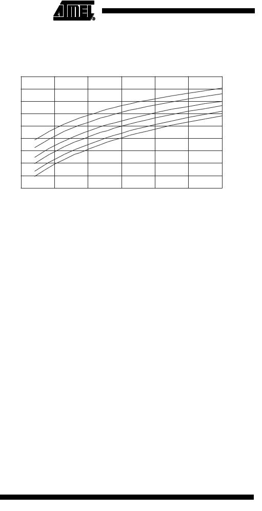
Figure 149. RC Oscillator Frequency vs. Operating Voltage (the devices are calibrated to 1 MHz at Vcc = 5V, T=25c)
CALIBRATED 1MHz RC OSCILLATOR FREQUENCY
vs. OPERATING VOLTAGE
|
1.03 |
|
|
|
|
|
|
|
1.02 |
|
|
|
|
TA = -40˚C |
TA = -10˚C |
|
|
|
|
|
|
||
|
1.01 |
|
|
|
|
|
TA = 25˚C |
|
|
|
|
|
|
|
TA = 45˚C |
|
1 |
|
|
|
|
|
TA = 70˚C |
|
0.99 |
|
|
|
|
TA = 85˚C |
|
|
0.98 |
|
|
|
|
|
|
(MHz) |
|
|
|
|
|
|
|
0.97 |
|
|
|
|
|
|
|
Rc |
|
|
|
|
|
|
|
F |
0.96 |
|
|
|
|
|
|
|
|
|
|
|
|
|
|
|
0.95 |
|
|
|
|
|
|
|
0.94 |
|
|
|
|
|
|
|
0.93 |
|
|
|
|
|
|
|
0.92 |
|
|
|
|
|
|
|
2.5 |
3 |
3.5 |
4 |
4.5 |
5 |
5.5 |
Vcc(V)
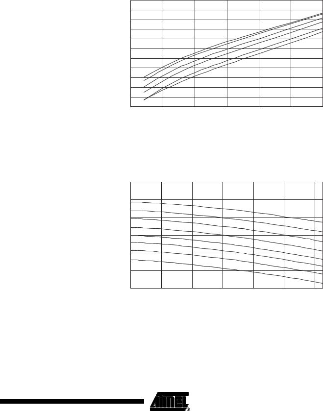
Figure 150. RC Oscillator Frequency vs. Temperature (the devices are calibrated to 2 MHz at Vcc = 5V, T=25c)
CALIBRATED 2MHz RC OSCILLATOR FREQUENCY
vs. TEMPERATURE
|
2.1 |
|
|
|
|
|
|
|
|
2.05 |
|
|
|
|
|
|
|
|
2 |
|
|
|
|
|
Vcc = 5.5V |
|
|
|
|
|
|
|
|
||
(MHz) |
1.95 |
|
|
|
|
|
Vcc = 5.0V |
|
|
|
|
|
|
|
|
||
|
|
|
|
|
|
Vcc |
= 4.5V |
|
Rc |
|
|
|
|
|
|
||
F |
|
|
|
|
|
|
Vcc = 4.0V |
|
|
1.9 |
|
|
|
|
|
||
|
|
|
|
|
|
|
|
|
|
|
|
|
|
|
|
Vcc = 3.6V |
|
|
1.85 |
|
|
|
|
|
Vcc = 3.3V |
|
|
|
|
|
|
|
Vcc |
= 3.0V |
|
|
|
|
|
|
|
|
||
|
1.8 |
|
|
|
|
|
Vcc = 2.7V |
|
|
|
|
|
|
|
|
|
|
|
-40 |
-20 |
0 |
20 |
40 |
60 |
80 |
|
|
|
|
|
Ta(˚C) |
|
|
|
|
295
2503F–AVR–12/03
Figure 151. RC Oscillator Frequency vs. Operating Voltage (the devices are calibrated to 2 MHz at Vcc = 5V, T=25c)
CALIBRATED 2MHz RC OSCILLATOR FREQUENCY
vs. OPERATING VOLTAGE
|
2.1 |
|
|
|
|
|
|
|
2.05 |
|
|
|
|
|
TA = -10˚C |
|
|
|
|
|
|
TA = -40˚C |
|
|
|
|
|
|
|
|
TA = 25˚C |
|
2 |
|
|
|
|
|
TA = 45˚C |
|
|
|
|
|
|
TA = 70˚C |
|
(MHz) |
1.95 |
|
|
|
|
|
TA = 85˚C |
|
|
|
|
|
|
||
|
|
|
|
|
|
|
|
Rc |
|
|
|
|
|
|
|
F |
|
|
|
|
|
|
|
|
1.9 |
|
|
|
|
|
|
|
1.85 |
|
|
|
|
|
|
|
1.8 |
|
|
|
|
|
|
|
2.5 |
3 |
3.5 |
4 |
4.5 |
5 |
5.5 |
Vcc(V)
Figure 152. RC Oscillator Frequency vs. Temperature (the devices are calibrated to 4 MHz at Vcc = 5V, T=25c)
CALIBRATED 4MHz RC OSCILLATOR FREQUENCY
vs. TEMPERATURE
|
4.1 |
|
|
|
|
|
|
|
4.05 |
|
|
|
|
|
|
|
4 |
|
|
|
|
|
|
|
3.95 |
|
|
|
|
|
Vcc = 5.5V |
|
|
|
|
|
|
Vcc = 5.0V |
|
|
|
|
|
|
|
|
|
|
3.9 |
|
|
|
|
|
Vcc = 4.5V |
|
|
|
|
|
|
|
|
(MHz) |
3.85 |
|
|
|
|
|
Vcc = 4.0V |
|
|
|
|
|
|
|
|
Rc |
3.8 |
|
|
|
|
|
V = 3.6V |
F |
|
|
|
|
|
||
|
|
|
|
|
cc |
||
|
3.75 |
|
|
|
|
|
Vcc = 3.3V |
|
|
|
|
|
|
|
|
|
3.7 |
|
|
|
|
|
Vcc = 3.0V |
|
|
|
|
|
|
|
|
|
3.65 |
|
|
|
|
|
Vcc = 2.7V |
|
|
|
|
|
|
|
|
|
3.6 |
|
|
|
|
|
|
|
-40 |
-20 |
0 |
20 |
40 |
60 |
80 |
|
|
|
|
Ta(˚C) |
|
|
|
296 ATmega32(L)
2503F–AVR–12/03
ATmega32(L)
Figure 153. RC Oscillator Frequency vs. Operating Voltage (the devices are calibrated to 4 MHz at Vcc = 5V, T=25c)
Rc
F (MHz)
CALIBRATED 4MHz RC OSCILLATOR FREQUENCY vs. OPERATING VOLTAGE
4.1
4.05 |
|
|
|
|
|
TA = -40˚C |
|
|
|
|
|
TA = -10˚C |
|
|
|
|
|
|
|
|
4 |
|
|
|
|
|
TA = 25˚C |
|
|
|
|
|
TA = 45˚C |
|
|
|
|
|
|
|
|
3.95 |
|
|
|
|
|
TA = 70˚C |
|
|
|
|
|
|
|
3.9 |
|
|
|
|
|
TA = 85˚C |
|
|
|
|
|
|
|
3.85 |
|
|
|
|
|
|
3.8 |
|
|
|
|
|
|
3.75 |
|
|
|
|
|
|
3.7 |
|
|
|
|
|
|
3.65 |
|
|
|
|
|
|
3.6 |
|
|
|
|
|
|
2.5 |
3 |
3.5 |
4 |
4.5 |
5 |
5.5 |
Vcc(V)
Figure 154. RC Oscillator Frequency vs. Temperature (the devices are calibrated to 8
MHz at Vcc = 5V, T=25c)
CALIBRATED 8MHz RC OSCILLATOR FREQUENCY
vs. TEMPERATURE
|
8.5 |
|
|
|
|
|
|
|
8.3 |
|
|
|
|
|
|
|
8.1 |
|
|
|
|
|
|
|
7.9 |
|
|
|
|
|
Vcc = 5.5V |
|
|
|
|
|
|
|
|
|
7.7 |
|
|
|
|
|
Vcc = 5.0V |
(MHz) |
|
|
|
|
|
Vcc = 4.5V |
|
|
|
|
|
|
|
||
7.5 |
|
|
|
|
|
Vcc = 4.0V |
|
Rc |
|
|
|
|
|
|
|
F |
|
|
|
|
|
|
Vcc = 3.6V |
|
7.3 |
|
|
|
|
|
|
|
|
|
|
|
|
Vcc = 3.3V |
|
|
|
|
|
|
|
|
|
|
7.1 |
|
|
|
|
|
Vcc = 3.0V |
|
6.9 |
|
|
|
|
|
Vcc = 2.7V |
|
|
|
|
|
|
|
|
|
6.7 |
|
|
|
|
|
|
|
-40 |
-20 |
0 |
20 |
40 |
60 |
80 |
|
|
|
|
Ta(˚C) |
|
|
|
297
2503F–AVR–12/03
Figure 155. RC Oscillator Frequency vs. Operating Voltage (the devices are calibrated to 8 MHz at Vcc = 5V, T=25c)
CALIBRATED 8MHz RC OSCILLATOR FREQUENCY
vs. OPERATING VOLTAGE
|
8.5 |
|
|
|
|
|
|
|
8.3 |
|
|
|
|
TA = -40˚C |
|
|
|
|
|
|
|
TA = -10˚C |
|
|
|
|
|
|
|
|
|
|
8.1 |
|
|
|
|
|
TA = 25˚C |
|
|
|
|
|
|
|
TA = 45˚C |
|
7.9 |
|
|
|
|
|
TA = 70˚C |
|
7.7 |
|
|
|
|
|
TA = 85˚C |
(MHz) |
|
|
|
|
|
|
|
7.5 |
|
|
|
|
|
|
|
Rc |
|
|
|
|
|
|
|
F |
|
|
|
|
|
|
|
|
7.3 |
|
|
|
|
|
|
|
7.1 |
|
|
|
|
|
|
|
6.9 |
|
|
|
|
|
|
|
6.7 |
|
|
|
|
|
|
|
2.5 |
3 |
3.5 |
4 |
4.5 |
5 |
5.5 |
Vcc(V)
298 ATmega32(L)
2503F–AVR–12/03