

- •Features
- •Pin Configurations
- •Disclaimer
- •Overview
- •Block Diagram
- •Pin Descriptions
- •Port A (PA7..PA0)
- •Port B (PB7..PB0)
- •Port C (PC7..PC0)
- •Port D (PD7..PD0)
- •RESET
- •XTAL1
- •XTAL2
- •AVCC
- •AREF
- •AVR CPU Core
- •Introduction
- •Architectural Overview
- •Status Register
- •Stack Pointer
- •Interrupt Response Time
- •SRAM Data Memory
- •Data Memory Access Times
- •EEPROM Data Memory
- •EEPROM Read/Write Access
- •I/O Memory
- •Clock Systems and their Distribution
- •CPU Clock – clkCPU
- •I/O Clock – clkI/O
- •Flash Clock – clkFLASH
- •ADC Clock – clkADC
- •Clock Sources
- •Default Clock Source
- •Crystal Oscillator
- •External RC Oscillator
- •External Clock
- •Timer/Counter Oscillator
- •Idle Mode
- •Power-down Mode
- •Power-save Mode
- •Standby Mode
- •Extended Standby Mode
- •Analog to Digital Converter
- •Analog Comparator
- •Brown-out Detector
- •Internal Voltage Reference
- •Watchdog Timer
- •Port Pins
- •Resetting the AVR
- •Reset Sources
- •Power-on Reset
- •External Reset
- •Brown-out Detection
- •Watchdog Reset
- •Watchdog Timer
- •Interrupts
- •I/O Ports
- •Introduction
- •Configuring the Pin
- •Reading the Pin Value
- •Unconnected pins
- •Alternate Port Functions
- •Alternate Functions of Port A
- •Alternate Functions of Port B
- •Alternate Functions of Port C
- •Alternate Functions of Port D
- •Port A Data Register – PORTA
- •Port B Data Register – PORTB
- •Port C Data Register – PORTC
- •Port D Data Register – PORTD
- •External Interrupts
- •8-bit Timer/Counter0 with PWM
- •Overview
- •Registers
- •Definitions
- •Counter Unit
- •Output Compare Unit
- •Force Output Compare
- •Modes of Operation
- •Normal Mode
- •Fast PWM Mode
- •Phase Correct PWM Mode
- •Internal Clock Source
- •Prescaler Reset
- •External Clock Source
- •16-bit Timer/Counter1
- •Overview
- •Registers
- •Definitions
- •Compatibility
- •Counter Unit
- •Input Capture Unit
- •Input Capture Trigger Source
- •Noise Canceler
- •Using the Input Capture Unit
- •Output Compare Units
- •Force Output Compare
- •Modes of Operation
- •Normal Mode
- •Fast PWM Mode
- •Phase Correct PWM Mode
- •8-bit Timer/Counter2 with PWM and Asynchronous Operation
- •Overview
- •Registers
- •Definitions
- •Counter Unit
- •Output Compare Unit
- •Force Output Compare
- •Modes of Operation
- •Normal Mode
- •Fast PWM Mode
- •Phase Correct PWM Mode
- •Timer/Counter Prescaler
- •SS Pin Functionality
- •Slave Mode
- •Master Mode
- •SPI Control Register – SPCR
- •SPI Status Register – SPSR
- •SPI Data Register – SPDR
- •Data Modes
- •USART
- •Overview
- •AVR USART vs. AVR UART – Compatibility
- •Clock Generation
- •External Clock
- •Synchronous Clock Operation
- •Frame Formats
- •Parity Bit Calculation
- •USART Initialization
- •Parity Generator
- •Disabling the Transmitter
- •Receiver Error Flags
- •Parity Checker
- •Disabling the Receiver
- •Flushing the Receive Buffer
- •Asynchronous Data Recovery
- •Using MPCM
- •Write Access
- •Read Access
- •Two-wire Serial Interface
- •Features
- •TWI Terminology
- •Electrical Interconnection
- •Transferring Bits
- •START and STOP Conditions
- •Address Packet Format
- •Data Packet Format
- •Overview of the TWI Module
- •SCL and SDA Pins
- •Bit Rate Generator Unit
- •Bus Interface Unit
- •Address Match Unit
- •Control Unit
- •TWI Register Description
- •TWI Bit Rate Register – TWBR
- •TWI Control Register – TWCR
- •TWI Status Register – TWSR
- •TWI Data Register – TWDR
- •Using the TWI
- •Transmission Modes
- •Master Transmitter Mode
- •Master Receiver Mode
- •Slave Receiver Mode
- •Slave Transmitter Mode
- •Miscellaneous States
- •Analog Comparator
- •Analog Comparator Multiplexed Input
- •Features
- •Operation
- •Starting a Conversion
- •Differential Gain Channels
- •Changing Channel or Reference Selection
- •ADC Input Channels
- •ADC Voltage Reference
- •ADC Noise Canceler
- •Analog Input Circuitry
- •ADC Accuracy Definitions
- •ADC Conversion Result
- •ADLAR = 0
- •ADLAR = 1
- •Features
- •Overview
- •Test Access Port – TAP
- •TAP Controller
- •PRIVATE0; $8
- •PRIVATE1; $9
- •PRIVATE2; $A
- •PRIVATE3; $B
- •Bibliography
- •Features
- •System Overview
- •Data Registers
- •Bypass Register
- •Device Identification Register
- •Reset Register
- •Boundary-scan Chain
- •EXTEST; $0
- •IDCODE; $1
- •SAMPLE_PRELOAD; $2
- •AVR_RESET; $C
- •BYPASS; $F
- •Scanning the Digital Port Pins
- •Scanning the RESET Pin
- •Scanning the Clock Pins
- •Scanning the ADC
- •Features
- •Application Section
- •BLS – Boot Loader Section
- •Read-While-Write and no Read-While-Write Flash Sections
- •Boot Loader Lock Bits
- •Performing a Page Write
- •Using the SPM Interrupt
- •Setting the Boot Loader Lock Bits by SPM
- •Reading the Fuse and Lock Bits from Software
- •Preventing Flash Corruption
- •Fuse Bits
- •Latching of Fuses
- •Signature Bytes
- •Calibration Byte
- •Signal Names
- •Parallel Programming
- •Enter Programming Mode
- •Chip Erase
- •Programming the Flash
- •Programming the EEPROM
- •Reading the Flash
- •Reading the EEPROM
- •Programming the Lock Bits
- •Reading the Signature Bytes
- •Reading the Calibration Byte
- •SPI Serial Downloading
- •Data Polling Flash
- •Data Polling EEPROM
- •AVR_RESET ($C)
- •PROG_ENABLE ($4)
- •PROG_COMMANDS ($5)
- •PROG_PAGELOAD ($6)
- •PROG_PAGEREAD ($7)
- •Data Registers
- •Reset Register
- •Programming Enable Register
- •Virtual Flash Page Read Register
- •Programming Algorithm
- •Entering Programming Mode
- •Leaving Programming Mode
- •Performing Chip Erase
- •Programming the Flash
- •Reading the Flash
- •Programming the EEPROM
- •Reading the EEPROM
- •Programming the Fuses
- •Programming the Lock Bits
- •Reading the Signature Bytes
- •Reading the Calibration Byte
- •Electrical Characteristics
- •Absolute Maximum Ratings*
- •DC Characteristics
- •External Clock Drive Waveforms
- •External Clock Drive
- •Two-wire Serial Interface Characteristics
- •ADC Characteristics
- •Register Summary
- •Instruction Set Summary
- •Ordering Information
- •Packaging Information
- •Errata
- •ATmega32 Rev. A
- •Datasheet Change Log for ATmega32
- •Changes from Rev. 2503E-09/03 to Rev. 2503F-12/03
- •Changes from Rev. 2503D-02/03 to Rev. 2503E-09/03
- •Changes from Rev. 2503C-10/02 to Rev. 2503D-02/03
- •Changes from Rev. 2503B-10/02 to Rev. 2503C-10/02
- •Changes from Rev. 2503A-03/02 to Rev. 2503B-10/02
- •Table of Contents
 ATmega32(L)
Overview
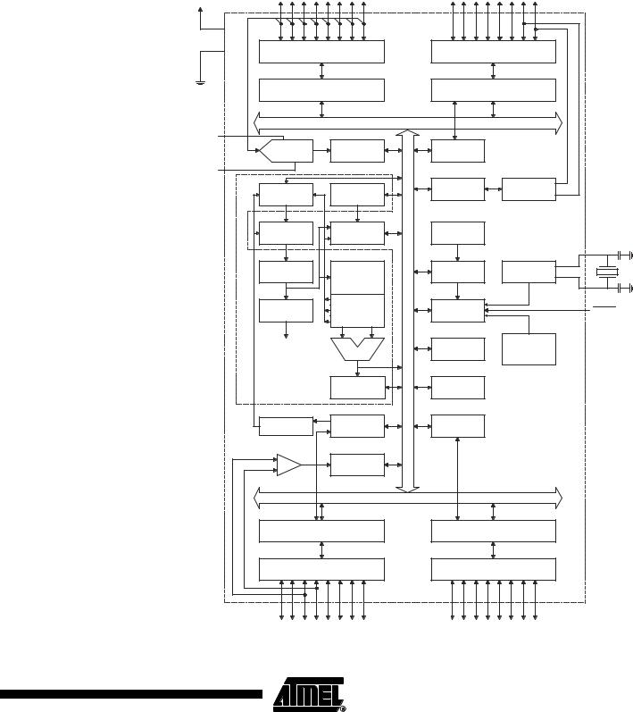
The ATmega32 is a low-power CMOS 8-bit microcontroller based on the AVR enhanced RISC architecture. By executing powerful instructions in a single clock cycle, the ATmega32 achieves throughputs approaching 1 MIPS per MHz allowing the system designer to optimize power consumption versus processing speed.
Block Diagram |
Figure 2. Block Diagram |
PA0 - PA7
VCC
|
PORTA DRIVERS/BUFFERS |
|
GND |
PORTA DIGITAL INTERFACE |
|
AVCC |
|
|
|
MUX & |
ADC |
|
ADC |
INTERFACE |
|
|
|
AREF |
|
|
|
PROGRAM |
STACK |
|
COUNTER |
POINTER |
|
PROGRAM |
SRAM |
|
FLASH |
|
|
|
|
|
INSTRUCTION |
GENERAL |
|
REGISTER |
|
|
PURPOSE |
|
|
|
REGISTERS |
|
|
X |
|
INSTRUCTION |
Y |
|
DECODER |
|
|
|
|
|
|
Z |
|
CONTROL |
|
|
LINES |
ALU |
|
AVR CPU |
STATUS |
|
REGISTER |
|
|
|
|
|
PROGRAMMING |
SPI |
|
LOGIC |
|
|
|
|
|
+ |
COMP. |
|
- |
INTERFACE |
|
PORTB DIGITAL INTERFACE |
|
|
PORTB DRIVERS/BUFFERS |
|
|
|
PB0 - PB7 |
|
PC0 - PC7 |
|
PORTC DRIVERS/BUFFERS |
|
|
PORTC DIGITAL INTERFACE |
|
|
TWI |
|
|
TIMERS/ |
OSCILLATOR |
|
COUNTERS |
|
|
|
|
|
INTERNAL |
|
|
OSCILLATOR |
|
|
|
|
XTAL1 |
WATCHDOG |
OSCILLATOR |
|
TIMER |
|
|
|
|
|
|
|
XTAL2 |
MCU CTRL. |
|
RESET |
& TIMING |
|
|
|
|
|
INTERRUPT |
INTERNAL |
|
CALIBRATED |
|
|
UNIT |
|
|
OSCILLATOR |
|
|
|
|
|
EEPROM |
|
|
USART |
|
|
PORTD DIGITAL INTERFACE
PORTD DRIVERS/BUFFERS
PD0 - PD7
3
2503F–AVR–12/03