

- •Features
- •Pin Configurations
- •Overview
- •Block Diagram
- •Disclaimer
- •Pin Descriptions
- •Port A (PA7..PA0)
- •Port B (PB7..PB0)
- •Port C (PC7..PC0)
- •Port D (PD7..PD0)
- •Port E(PE2..PE0)
- •RESET
- •XTAL1
- •XTAL2
- •AVR CPU Core
- •Introduction
- •Architectural Overview
- •Status Register
- •Stack Pointer
- •Interrupt Response Time
- •In-System Reprogrammable Flash Program memory
- •SRAM Data Memory
- •Data Memory Access Times
- •EEPROM Data Memory
- •EEPROM Read/Write Access
- •I/O Memory
- •Overview
- •Address Latch Requirements
- •Pull-up and Bus Keeper
- •Timing
- •Using all Locations of External Memory Smaller than 64 KB
- •Using all 64KB Locations of External Memory
- •Clock Systems and their Distribution
- •Clock Sources
- •Default Clock Source
- •Crystal Oscillator
- •External RC Oscillator
- •External Clock
- •Idle Mode
- •Power-down Mode
- •Standby Mode
- •Analog Comparator
- •Brown-out Detector
- •Internal Voltage Reference
- •Watchdog Timer
- •Port Pins
- •Resetting the AVR
- •Reset Sources
- •Power-on Reset
- •External Reset
- •Brown-out Detection
- •Watchdog Reset
- •Watchdog Timer
- •Timed Sequences for Changing the Configuration of the Watchdog Timer
- •Safety Level 0
- •Safety Level 1
- •Safety Level 2
- •Interrupts
- •Moving Interrupts between Application and Boot Space
- •I/O Ports
- •Introduction
- •Configuring the Pin
- •Reading the Pin Value
- •Unconnected pins
- •Alternate Port Functions
- •Alternate Functions of Port A
- •Alternate Functions Of Port B
- •Alternate Functions of Port C
- •Alternate Functions of Port D
- •Alternate Functions of Port E
- •Register Description for I/O Ports
- •External Interrupts
- •8-bit Timer/Counter0 with PWM
- •Overview
- •Registers
- •Definitions
- •Counter Unit
- •Output Compare Unit
- •Force Output Compare
- •Modes of Operation
- •Normal Mode
- •Fast PWM Mode
- •Phase Correct PWM Mode
- •Internal Clock Source
- •Prescaler Reset
- •External Clock Source
- •16-bit Timer/Counter1
- •Overview
- •Registers
- •Definitions
- •Compatibility
- •Counter Unit
- •Input Capture Unit
- •Input Capture Trigger Source
- •Noise Canceler
- •Using the Input Capture Unit
- •Output Compare Units
- •Force Output Compare
- •Modes of Operation
- •Normal Mode
- •Fast PWM Mode
- •Phase Correct PWM Mode
- •Slave Mode
- •Master Mode
- •Data Modes
- •USART
- •Single USART
- •Clock Generation
- •External Clock
- •Synchronous Clock Operation
- •Frame Formats
- •Parity Bit Calculation
- •USART Initialization
- •Sending Frames with 5 to 8 Data Bits
- •Sending Frames with 9 Data Bits
- •Parity Generator
- •Disabling the Transmitter
- •Receiving Frames with 5 to 8 Data Bits
- •Receiving Frames with 9 Data Bits
- •Receiver Error Flags
- •Parity Checker
- •Disabling the Receiver
- •Flushing the Receive Buffer
- •Asynchronous Data Recovery
- •Using MPCM
- •Write Access
- •Read Access
- •Analog Comparator
- •Features
- •Application Section
- •Boot Loader Lock bits
- •Performing a Page Write
- •Using the SPM Interrupt
- •Setting the Boot Loader Lock bits by SPM
- •Reading the Fuse and Lock bits from Software
- •Preventing Flash Corruption
- •Simple Assembly Code Example for a Boot Loader
- •Program and Data Memory Lock bits
- •Fuse bits
- •Latching of Fuses
- •Signature Bytes
- •Calibration Byte
- •Calibration Byte
- •Signal Names
- •Parallel Programming
- •Enter Programming Mode
- •Chip Erase
- •Programming the Flash
- •Programming the EEPROM
- •Reading the Flash
- •Reading the EEPROM
- •Programming the Lock bits
- •Reading the Signature Bytes
- •Reading the Calibration Byte
- •Serial Downloading
- •Data Polling Flash
- •Data Polling EEPROM
- •Electrical Characteristics
- •Absolute Maximum Ratings*
- •External Clock Drive Waveforms
- •External Clock Drive
- •External Data Memory Timing
- •Active Supply Current
- •Idle Supply Current
- •Standby Supply Current
- •Pin Pull-up
- •Pin Driver Strength
- •Internal Oscillator Speed
- •Register Summary
- •Instruction Set Summary
- •Ordering Information
- •Packaging Information
- •Errata
- •ATmega8515(L) Rev. B
- •Changes from Rev. 2512F-12/03 to Rev. 2512G-03/05
- •Changes from Rev. 2512F-12/03 to Rev. 2512E-09/03
- •Changes from Rev. 2512D-02/03 to Rev. 2512E-09/03
- •Changes from Rev. 2512C-10/02 to Rev. 2512D-02/03
- •Changes from Rev. 2512B-09/02 to Rev. 2512C-10/02
- •Changes from Rev. 2512A-04/02 to Rev. 2512B-09/02
- •Table of Contents

 ATmega8515(L)
ATmega8515 Typical
Characteristics
Active Supply Current
The following charts show typical behavior. These figures are not tested during manufacturing. All current consumption measurements are performed with all I/O pins configured as inputs and with internal pull-ups enabled. A sine wave generator with rail- to-rail output is used as clock source.
The power consumption in Power-down mode is independent of clock selection.
The current consumption is a function of several factors such as: Operating voltage, operating frequency, loading of I/O pins, switching rate of I/O pins, code executed and ambient temperature. The dominating factors are operating voltage and frequency.
The current drawn from capacitive loaded pins may be estimated (for one pin) as CL*VCC*f where CL = load capacitance, VCC = operating voltage and f = average switching frequency of I/O pin.
The parts are characterized at frequencies higher than test limits. Parts are not guaranteed to function properly at frequencies higher than the ordering code indicates.
The difference between current consumption in Power-down mode with Watchdog Timer enabled and Power-down mode with Watchdog Timer disabled represents the differential current drawn by the Watchdog Timer.
Figure 93. Active Supply Current vs. Frequency (0.1 - 1.0 MHz)
ACTIVE SUPPLY CURRENT vs. FREQUENCY
|
|
|
|
|
|
0.1 - 1.0 MHz |
|
|
|
|
|
|
1.6 |
|
|
|
|
|
|
|
|
|
|
|
1.4 |
|
|
|
|
|
|
|
|
|
5.5 V |
|
|
|
|
|
|
|
|
|
|
5.0 V |
|
|
|
|
|
|
|
|
|
|
|
|
|
|
1.2 |
|
|
|
|
|
|
|
|
|
4.5 V |
|
|
|
|
|
|
|
|
|
|
|
4.0 V |
|
1 |
|
|
|
|
|
|
|
|
|
3.3 V |
(mA) |
|
|
|
|
|
|
|
|
|
|
3.0 V |
0.8 |
|
|
|
|
|
|
|
|
|
2.7 V |
|
CC |
|
|
|
|
|
|
|
|
|
|
|
I |
|
|
|
|
|
|
|
|
|
|
|
|
0.6 |
|
|
|
|
|
|
|
|
|
|
|
0.4 |
|
|
|
|
|
|
|
|
|
|
|
0.2 |
|
|
|
|
|
|
|
|
|
|
|
0 |
|
|
|
|
|
|
|
|
|
|
|
0 |
0.1 |
0.2 |
0.3 |
0.4 |
0.5 |
0.6 |
0.7 |
0.8 |
0.9 |
1 |
Frequency (MHz)
205
2512G–AVR–03/05

Figure 94. Active Supply Current vs. Frequency (1 - 20 MHz)
ACTIVE SUPPLY CURRENT vs. FREQUENCY
|
|
|
|
|
|
1 - 20 MHz |
|
|
|
|
|
|
25 |
|
|
|
|
|
|
|
|
|
|
|
|
|
|
|
|
|
|
|
|
|
5.5 V |
|
20 |
|
|
|
|
|
|
|
|
|
5.0 V |
|
|
|
|
|
|
|
|
|
|
|
|
|
|
|
|
|
|
|
|
|
|
|
4.5 V |
(mA) |
15 |
|
|
|
|
|
|
|
|
|
|
|
|
|
|
|
|
|
|
|
|
|
|
CC |
|
|
|
|
|
|
|
|
|
4.0V |
|
I |
10 |
|
|
|
|
|
|
|
|
|
|
|
|
|
|
|
|
|
|
|
|
|
|
|
|
|
|
|
|
|
|
|
3.3V |
|
|
|
5 |
|
|
|
|
|
3.0V |
|
|
|
|
|
|
|
|
|
|
2.7V |
|
|
|
|
|
|
|
|
|
|
|
|
|
|
|
|
|
|
0 |
|
|
|
|
|
|
|
|
|
|
|
0 |
2 |
4 |
6 |
8 |
10 |
12 |
14 |
16 |
18 |
20 |
Frequency (MHz)
Figure 95. Active Supply Current vs. VCC (Internal RC Oscillator, 8 MHz)
ACTIVE SUPPLY CURRENT vs. VCC
INTERNAL RC OSCILLATOR, 8 MHz
|
14 |
|
|
|
|
|
|
|
12 |
|
|
|
|
|
-40 °C |
|
|
|
|
|
|
25 °C |
|
|
|
|
|
|
|
|
|
|
10 |
|
|
|
|
|
85 °C |
|
|
|
|
|
|
|
|
(mA) |
8 |
|
|
|
|
|
|
|
|
|
|
|
|
|
|
CC |
6 |
|
|
|
|
|
|
I |
|
|
|
|
|
|
|
|
|
|
|
|
|
|
|
|
4 |
|
|
|
|
|
|
|
2 |
|
|
|
|
|
|
|
0 |
|
|
|
|
|
|
|
2.5 |
3 |
3.5 |
4 |
4.5 |
5 |
5.5 |
VCC (V)
206 ATmega8515(L)
2512G–AVR–03/05

 ATmega8515(L)
Figure 96. Active Supply Current vs. VCC (Internal RC Oscillator, 4 MHz)
ACTIVE SUPPLY CURRENT vs. VCC
INTERNAL RC OSCILLATOR, 4 MHz
|
8 |
|
|
|
|
|
|
|
7 |
|
|
|
|
|
-40°C |
|
|
|
|
|
|
|
85°C |
|
6 |
|
|
|
|
|
25°C |
|
5 |
|
|
|
|
|
|
(mA) |
4 |
|
|
|
|
|
|
CC |
|
|
|
|
|
|
|
I |
|
|
|
|
|
|
|
|
3 |
|
|
|
|
|
|
|
2 |
|
|
|
|
|
|
|
1 |
|
|
|
|
|
|
|
0 |
|
|
|
|
|
|
|
2.5 |
3 |
3.5 |
4 |
4.5 |
5 |
5.5 |
VCC (V)
Figure 97. Active Supply Current vs. VCC (Internal RC Oscillator, 2 MHz)
ACTIVE SUPPLY CURRENT vs. VCC
INTERNAL RC OSCILLATOR, 2 MHz
|
4 |
|
|
|
|
|
|
|
3.5 |
|
|
|
|
|
85°C |
|
|
|
|
|
|
|
-40°C |
|
3 |
|
|
|
|
|
25°C |
|
2.5 |
|
|
|
|
|
|
(mA) |
2 |
|
|
|
|
|
|
CC |
|
|
|
|
|
|
|
I |
|
|
|
|
|
|
|
|
1.5 |
|
|
|
|
|
|
|
1 |
|
|
|
|
|
|
|
0.5 |
|
|
|
|
|
|
|
0 |
|
|
|
|
|
|
|
2.5 |
3 |
3.5 |
4 |
4.5 |
5 |
5.5 |
VCC (V)
207
2512G–AVR–03/05
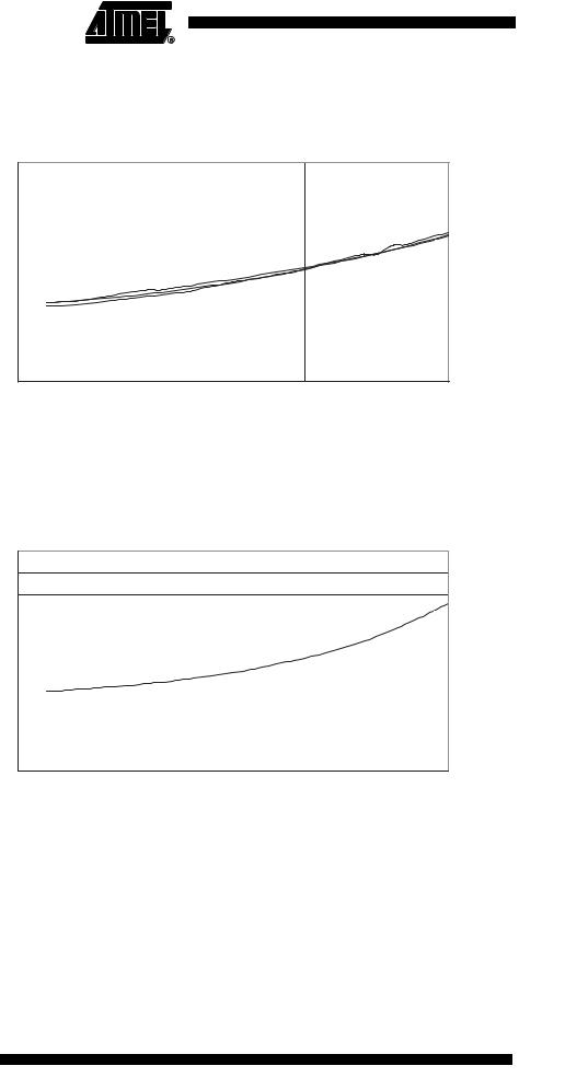
Figure 98. Active Supply Current vs. VCC (Internal RC Oscillator, 1 MHz)
ACTIVE SUPPLY CURRENT vs. VCC
INTERNAL RC OSCILLATOR, 1 MHz
2.5 |
|
|
|
|
|
|
2 |
|
|
|
|
|
85°C |
|
|
|
|
|
|
|
|
|
|
|
|
|
-40°C |
1.5 |
|
|
|
|
|
25°C |
|
|
|
|
|
|
|
(mA) |
|
|
|
|
|
|
CC |
|
|
|
|
|
|
I |
|
|
|
|
|
|
1 |
|
|
|
|
|
|
0.5 |
|
|
|
|
|
|
0 |
|
|
|
|
|
|
2.5 |
3 |
3.5 |
4 |
4.5 |
5 |
5.5 |
VCC (V)
Figure 99. Active Supply Current vs. VCC (32 kHz External Oscillator)
ACTIVE SUPPLY CURRENT vs. VCC
32kHz EXTERNAL OSCILLATOR
|
100 |
|
|
|
|
|
|
|
90 |
|
|
|
|
|
|
|
80 |
|
|
|
|
|
25°C |
|
|
|
|
|
|
|
|
|
70 |
|
|
|
|
|
|
(uA) |
60 |
|
|
|
|
|
|
50 |
|
|
|
|
|
|
|
CC |
|
|
|
|
|
|
|
|
|
|
|
|
|
|
|
I |
40 |
|
|
|
|
|
|
|
|
|
|
|
|
|
|
|
30 |
|
|
|
|
|
|
|
20 |
|
|
|
|
|
|
|
10 |
|
|
|
|
|
|
|
0 |
|
|
|
|
|
|
|
2.5 |
3 |
3.5 |
4 |
4.5 |
5 |
5.5 |
VCC (V)
208 ATmega8515(L)
2512G–AVR–03/05