


|
|
|
|
|
|
|
ATmega8515(L) |
|
|
|
|
|
|
|
|
|
Electrical Characteristics |
|
|||||
|
|
|
|||||
|
|
|
|||||
|
Absolute Maximum Ratings* |
|
|
||||
|
|
*NOTICE: Stresses beyond those listed under “Absolute |
|||||
|
Operating Temperature.................................. -55°C to +125°C |
||||||
|
|
|
|
|
|
Maximum Ratings” may cause permanent dam- |
|
|
Storage Temperature ..................................... -65°C to +150°C |
age to the device. This is a stress rating only and |
|||||
|
|
|
|
|
|
functional operation of the device at these or |
|
|
Voltage on any Pin except |
RESET |
|
other conditions beyond those indicated in the |
|||
|
with respect to Ground ................................-0.5V to VCC+0.5V |
operational sections of this specification is not |
|||||
|
Voltage on |
|
with respect to Ground......-0.5V to +13.0V |
implied. Exposure to absolute maximum rating |
|||
|
RESET |
conditions for extended periods may affect |
|||||
|
Maximum Operating Voltage ............................................ 6.0V |
device reliability. |
|||||
|
|
|
|||||
|
DC Current per I/O Pin ............................................... 40.0 mA |
|
|
||||
|
DC Current VCC and GND Pins................................ 200.0 mA |
|
|
||||
|
|
|
|
|
|
|
|
DC Characteristics
TA = -40°C to 85°C, VCC = 2.7V to 5.5V (Unless Otherwise Noted)
Symbol |
|
Parameter |
Condition |
|
Min |
|
Typ |
Max |
Units |
|||||
|
|
|
|
|
|
|
|
|
|
|
|
|||
|
|
Input Low Voltage except |
|
|
|
|
|
|
|
(1) |
|
|||
VIL |
|
XTAL1 and |
|
pins |
VCC=2.7V - 5.5V |
-0.5 |
|
|
0.2 VCC |
V |
||||
RESET |
|
|
||||||||||||
VIH |
|
Input High Voltage except |
VCC=2.7V - 5.5V |
0.6 VCC |
(2) |
|
VCC + 0.5 |
V |
||||||
|
XTAL1 and |
RESET |
pins |
|
|
|||||||||
VIL1 |
|
Input Low Voltage |
VCC=2.7V - 5.5V |
-0.5 |
|
|
(1) |
V |
||||||
|
XTAL1 pin |
|
|
0.1 VCC |
||||||||||
|
|
|
|
|
|
|
|
|
|
|
||||
|
|
|
|
|
|
|
|
|
|
|
|
|||
VIH1 |
|
Input High Voltage |
VCC=2.7V - 5.5V |
0.8 VCC |
(2) |
|
VCC + 0.5 |
V |
||||||
|
|
|
|
|
|
|||||||||
|
XTAL1 pin |
|
|
|||||||||||
|
|
|
|
|
|
|
|
|
|
|
||||
|
|
|
|
|
|
|
|
|
|
|
|
|||
VIL2 |
|
Input Low Voltage |
VCC=2.7V - 5.5V |
-0.5 |
|
|
0.2 VCC |
V |
||||||
|
|
|
|
|
|
|
||||||||
RESET pin |
|
|
||||||||||||
|
|
|
|
|
|
|
|
|
|
|
||||
|
|
|
|
|
|
|
|
|
|
|
|
|||
VIH2 |
|
Input High Voltage |
VCC=2.7V - 5.5V |
0.9 VCC |
(2) |
|
VCC + 0.5 |
V |
||||||
|
|
|
|
|
|
|||||||||
|
RESET pin |
|
|
|||||||||||
|
|
|
|
|
|
|
|
|
|
|
||||
|
|
|
|
|
|
|
|
|
|
|
|
|||
|
|
Output Low Voltage(3) |
I |
OL |
= 20 mA, V |
= 5V |
|
|
|
0.7 |
V |
|||
VOL |
|
|
|
|
|
|
|
CC |
|
|
|
|
|
|
|
(Ports A,B,C,D,E) |
IOL = 10 mA, VCC = 3V |
|
|
|
0.5 |
V |
|||||||
|
|
|
|
|
||||||||||
VOH |
|
Output High Voltage(4) |
IOH = -20 mA, VCC = 5V |
4.2 |
|
|
|
V |
||||||
|
(Ports A,B,C,D,E) |
IOH = -10 mA, VCC = 3V |
2.2 |
|
|
|
V |
|||||||
|
|
|
|
|
||||||||||
IIL |
|
Input Leakage |
VCC = 5.5V, pin low |
|
|
|
1 |
µA |
||||||
|
Current I/O Pin |
(absolute value) |
|
|
|
|||||||||
IIH |
|
Input Leakage |
VCC = 5.5V, pin high |
|
|
|
1 |
µA |
||||||
|
Current I/O Pin |
(absolute value) |
|
|
|
|||||||||
RRST |
|
Reset Pull-up Resistor |
|
|
|
|
30 |
|
|
60 |
kΩ |
|||
Rpu |
|
I/O Pin Pull-up Resistor |
|
|
|
|
20 |
|
|
50 |
kΩ |
|||
195
2512G–AVR–03/05

DC Characteristics (Continued)
TA = -40°C to 85°C, VCC = 2.7V to 5.5V (Unless Otherwise Noted)
Symbol |
Parameter |
Condition |
Min |
Typ |
Max |
Units |
|
|
|
|
|
|
|
|
|
Active 4 MHz, VCC = 3V |
|
|
4 |
mA |
|
|
(ATmega8515L) |
|
|
||
|
|
|
|
|
|
|
|
|
|
|
|
|
|
|
|
Active 8 MHz, VCC = 5V |
|
|
12 |
mA |
|
|
(ATmega8515) |
|
|
||
|
Power Supply Current |
|
|
|
|
|
|
|
|
|
|
|
|
ICC |
Idle 4 MHz, VCC = 3V |
|
|
1.5 |
mA |
|
|
|
|
||||
|
(ATmega8515L) |
|
|
|||
|
|
|
|
|
||
|
|
Idle 8 MHz, VCC = 5V |
|
|
5.5 |
mA |
|
|
(ATmega8515) |
|
|
||
|
|
|
|
|
|
|
|
|
|
|
|
|
|
|
Power-down mode(5) |
WDT enabled, VCC = 3V |
|
|
< 13 |
µA |
|
WDT disabled, VCC = 3V |
|
|
< 2 |
µA |
|
|
|
|
|
|||
VACIO |
Analog Comparator |
VCC = 5V |
|
|
40 |
mV |
Input Offset Voltage |
Vin = VCC/2 |
|
|
|||
|
|
|
|
|
||
IACLK |
Analog Comparator |
VCC = 5V |
-50 |
|
50 |
nA |
Input Leakage Current |
Vin = VCC/2 |
|
||||
|
|
|
|
|
||
tACPD |
Analog Comparator |
VCC = 2.7V |
|
750 |
|
ns |
Propagation Delay |
VCC = 4.0V |
|
500 |
|
||
|
|
|
|
Notes: 1. “Max” means the highest value where the pin is guaranteed to be read as low.
2.“Min” means the lowest value where the pin is guaranteed to be read as high.
3.Although each I/O port can sink more than the test conditions (20 mA at VCC = 5V, 10 mA at VCC = 3V) under steady state conditions (non-transient), the following must be observed:
1] The sum of all IOL, for all ports, should not exceed 200 mA.
2] The sum of all IOL, for ports B0 - B7, D0 - D7, and XTAL2, should not exceed 100 mA. 3] The sum of all IOL, for ports A0 - A7, E0 - E2, and C0 - C7 should not exceed 100 mA.
4.Although each I/O port can source more than the test conditions (20 mA at VCC = 5V, 10 mA at VCC = 3V) under steady state conditions (non-transient),the following must be observed:
1] The sum of all IOH,for all ports, should not exceed 200 mA.
2] The sum of all IOH,for ports B0 - B7, D0 - D7, and XTAL2,should not exceed 100 mA. 3] The sum of all IOH,for ports A0 - A7, E0 - E2, and C0 - C7 should not exceed 100 mA.
5.Minimum VCC for Power-down is 2.5V.
196 ATmega8515(L)
2512G–AVR–03/05
 ATmega8515(L)
ATmega8515(L)
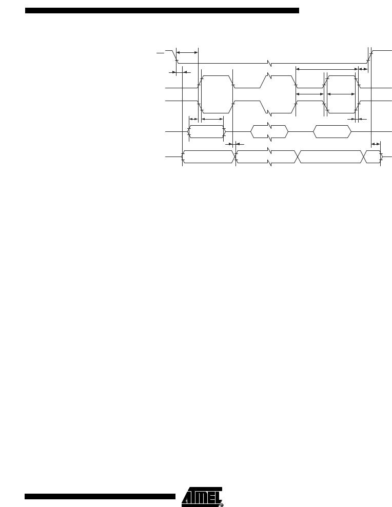
Figure 88. SPI Interface Timing Requirements (Slave Mode)
18 |
|
|
|
|
|
SS |
|
|
|
|
|
9 |
|
|
10 |
16 |
|
|
|
|
|
||
SCK |
|
|
|
|
|
(CPOL = 0) |
|
|
|
|
|
|
|
11 |
11 |
|
|
SCK |
|
|
|
|
|
(CPOL = 1) |
|
|
|
|
|
13 |
14 |
|
|
12 |
|
MOSI |
MSB |
... |
LSB |
|
|
(Data Input) |
|
||||
|
|
|
|
||
|
|
15 |
|
17 |
|
MISO |
MSB |
... |
LSB |
X |
|
(Data Output) |
|||||
|
|
|
|
199
2512G–AVR–03/05