

- •Features
- •Pin Configurations
- •Overview
- •Block Diagram
- •Disclaimer
- •Pin Descriptions
- •Port A (PA7..PA0)
- •Port B (PB7..PB0)
- •Port C (PC7..PC0)
- •Port D (PD7..PD0)
- •Port E(PE2..PE0)
- •RESET
- •XTAL1
- •XTAL2
- •AVR CPU Core
- •Introduction
- •Architectural Overview
- •Status Register
- •Stack Pointer
- •Interrupt Response Time
- •In-System Reprogrammable Flash Program memory
- •SRAM Data Memory
- •Data Memory Access Times
- •EEPROM Data Memory
- •EEPROM Read/Write Access
- •I/O Memory
- •Overview
- •Address Latch Requirements
- •Pull-up and Bus Keeper
- •Timing
- •Using all Locations of External Memory Smaller than 64 KB
- •Using all 64KB Locations of External Memory
- •Clock Systems and their Distribution
- •Clock Sources
- •Default Clock Source
- •Crystal Oscillator
- •External RC Oscillator
- •External Clock
- •Idle Mode
- •Power-down Mode
- •Standby Mode
- •Analog Comparator
- •Brown-out Detector
- •Internal Voltage Reference
- •Watchdog Timer
- •Port Pins
- •Resetting the AVR
- •Reset Sources
- •Power-on Reset
- •External Reset
- •Brown-out Detection
- •Watchdog Reset
- •Watchdog Timer
- •Timed Sequences for Changing the Configuration of the Watchdog Timer
- •Safety Level 0
- •Safety Level 1
- •Safety Level 2
- •Interrupts
- •Moving Interrupts between Application and Boot Space
- •I/O Ports
- •Introduction
- •Configuring the Pin
- •Reading the Pin Value
- •Unconnected pins
- •Alternate Port Functions
- •Alternate Functions of Port A
- •Alternate Functions Of Port B
- •Alternate Functions of Port C
- •Alternate Functions of Port D
- •Alternate Functions of Port E
- •Register Description for I/O Ports
- •External Interrupts
- •8-bit Timer/Counter0 with PWM
- •Overview
- •Registers
- •Definitions
- •Counter Unit
- •Output Compare Unit
- •Force Output Compare
- •Modes of Operation
- •Normal Mode
- •Fast PWM Mode
- •Phase Correct PWM Mode
- •Internal Clock Source
- •Prescaler Reset
- •External Clock Source
- •16-bit Timer/Counter1
- •Overview
- •Registers
- •Definitions
- •Compatibility
- •Counter Unit
- •Input Capture Unit
- •Input Capture Trigger Source
- •Noise Canceler
- •Using the Input Capture Unit
- •Output Compare Units
- •Force Output Compare
- •Modes of Operation
- •Normal Mode
- •Fast PWM Mode
- •Phase Correct PWM Mode
- •Slave Mode
- •Master Mode
- •Data Modes
- •USART
- •Single USART
- •Clock Generation
- •External Clock
- •Synchronous Clock Operation
- •Frame Formats
- •Parity Bit Calculation
- •USART Initialization
- •Sending Frames with 5 to 8 Data Bits
- •Sending Frames with 9 Data Bits
- •Parity Generator
- •Disabling the Transmitter
- •Receiving Frames with 5 to 8 Data Bits
- •Receiving Frames with 9 Data Bits
- •Receiver Error Flags
- •Parity Checker
- •Disabling the Receiver
- •Flushing the Receive Buffer
- •Asynchronous Data Recovery
- •Using MPCM
- •Write Access
- •Read Access
- •Analog Comparator
- •Features
- •Application Section
- •Boot Loader Lock bits
- •Performing a Page Write
- •Using the SPM Interrupt
- •Setting the Boot Loader Lock bits by SPM
- •Reading the Fuse and Lock bits from Software
- •Preventing Flash Corruption
- •Simple Assembly Code Example for a Boot Loader
- •Program and Data Memory Lock bits
- •Fuse bits
- •Latching of Fuses
- •Signature Bytes
- •Calibration Byte
- •Calibration Byte
- •Signal Names
- •Parallel Programming
- •Enter Programming Mode
- •Chip Erase
- •Programming the Flash
- •Programming the EEPROM
- •Reading the Flash
- •Reading the EEPROM
- •Programming the Lock bits
- •Reading the Signature Bytes
- •Reading the Calibration Byte
- •Serial Downloading
- •Data Polling Flash
- •Data Polling EEPROM
- •Electrical Characteristics
- •Absolute Maximum Ratings*
- •External Clock Drive Waveforms
- •External Clock Drive
- •External Data Memory Timing
- •Active Supply Current
- •Idle Supply Current
- •Standby Supply Current
- •Pin Pull-up
- •Pin Driver Strength
- •Internal Oscillator Speed
- •Register Summary
- •Instruction Set Summary
- •Ordering Information
- •Packaging Information
- •Errata
- •ATmega8515(L) Rev. B
- •Changes from Rev. 2512F-12/03 to Rev. 2512G-03/05
- •Changes from Rev. 2512F-12/03 to Rev. 2512E-09/03
- •Changes from Rev. 2512D-02/03 to Rev. 2512E-09/03
- •Changes from Rev. 2512C-10/02 to Rev. 2512D-02/03
- •Changes from Rev. 2512B-09/02 to Rev. 2512C-10/02
- •Changes from Rev. 2512A-04/02 to Rev. 2512B-09/02
- •Table of Contents
 ATmega8515(L)
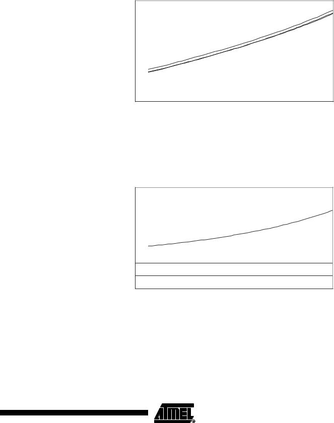
Figure 108. Power-Down Supply Current vs. VCC (Watchdog Timer Enabled)
POWER-DOWN SUPPLY CURRENT vs. VCC
WATCHDOG TIMER ENABLED
|
20 |
|
|
|
|
|
85°C |
|
|
|
|
|
|
|
|
|
18 |
|
|
|
|
|
-40°C |
|
16 |
|
|
|
|
|
25°C |
|
|
|
|
|
|
|
|
|
14 |
|
|
|
|
|
|
(uA) |
12 |
|
|
|
|
|
|
10 |
|
|
|
|
|
|
|
CC |
|
|
|
|
|
|
|
|
|
|
|
|
|
|
|
I |
8 |
|
|
|
|
|
|
|
|
|
|
|
|
|
|
|
6 |
|
|
|
|
|
|
|
4 |
|
|
|
|
|
|
|
2 |
|
|
|
|
|
|
|
0 |
|
|
|
|
|
|
|
2.5 |
3 |
3.5 |
4 |
4.5 |
5 |
5.5 |
VCC (V)
Standby Supply Current |
Figure 109. Standby Supply Current vs. VCC (455 kHz Resonator, Watchdog Timer |
Disabled)
STANDBY SUPPLY CURRENT vs. VCC
455 kHz RESONATOR, WATCHDOG TIMER DISABLED
|
80 |
|
|
|
|
|
|
|
70 |
|
|
|
|
|
|
|
60 |
|
|
|
|
|
|
|
50 |
|
|
|
|
|
|
(uA) |
40 |
|
|
|
|
|
|
CC |
|
|
|
|
|
|
|
I |
|
|
|
|
|
|
|
|
30 |
|
|
|
|
|
|
|
20 |
|
|
|
|
|
|
|
10 |
|
|
|
|
|
|
|
0 |
|
|
|
|
|
|
|
2.5 |
3 |
3.5 |
4 |
4.5 |
5 |
5.5 |
VCC (V)
213
2512G–AVR–03/05
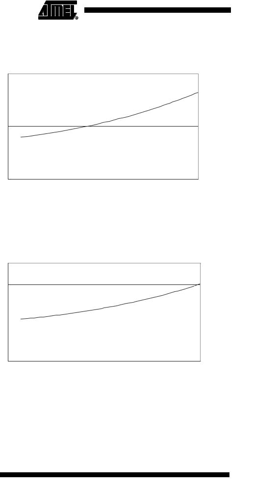
Figure 110. Standby Supply Current vs. VCC (1 MHz Resonator, Watchdog Timer
Disabled)
STANDBY SUPPLY CURRENT vs. VCC
1 MHz RESONATOR, WATCHDOG TIMER DISABLED
|
60 |
|
|
|
|
|
|
|
50 |
|
|
|
|
|
|
|
40 |
|
|
|
|
|
|
(uA) |
30 |
|
|
|
|
|
|
CC |
|
|
|
|
|
|
|
|
|
|
|
|
|
|
|
I |
|
|
|
|
|
|
|
|
20 |
|
|
|
|
|
|
|
10 |
|
|
|
|
|
|
|
0 |
|
|
|
|
|
|
|
2.5 |
3 |
3.5 |
4 |
4.5 |
5 |
5.5 |
VCC (V)
Figure 111. Standby Supply Current vs. VCC (2 MHz Resonator, Watchdog Timer
Disabled)
STANDBY SUPPLY CURRENT vs. VCC
2 MHz RESONATOR, WATCHDOG TIMER DISABLED
|
90 |
|
|
|
|
|
|
|
80 |
|
|
|
|
|
|
|
70 |
|
|
|
|
|
|
|
60 |
|
|
|
|
|
|
(uA) |
50 |
|
|
|
|
|
|
|
|
|
|
|
|
|
|
CC |
40 |
|
|
|
|
|
|
I |
|
|
|
|
|
|
|
|
30 |
|
|
|
|
|
|
|
20 |
|
|
|
|
|
|
|
10 |
|
|
|
|
|
|
|
0 |
|
|
|
|
|
|
|
2.5 |
3 |
3.5 |
4 |
4.5 |
5 |
5.5 |
VCC (V)
214 ATmega8515(L)
2512G–AVR–03/05

 ATmega8515(L)
Figure 112. Standby Supply Current vs. VCC (2 MHz XTAL, Watchdog Timer Disabled)
STANDBY SUPPLY CURRENT vs. VCC
2 MHz XTAL, WATCHDOG TIMER DISABLED
|
100 |
|
|
|
|
|
|
|
90 |
|
|
|
|
|
|
|
80 |
|
|
|
|
|
|
|
70 |
|
|
|
|
|
|
(uA) |
60 |
|
|
|
|
|
|
50 |
|
|
|
|
|
|
|
CC |
|
|
|
|
|
|
|
I |
40 |
|
|
|
|
|
|
|
|
|
|
|
|
|
|
|
30 |
|
|
|
|
|
|
|
20 |
|
|
|
|
|
|
|
10 |
|
|
|
|
|
|
|
0 |
|
|
|
|
|
|
|
2.5 |
3 |
3.5 |
4 |
4.5 |
5 |
5.5 |
VCC (V)
Figure 113. Standby Supply Current vs. VCC (4 MHz Resonator, Watchdog Timer
Disabled)
STANDBY SUPPLY CURRENT vs. VCC
4 MHz RESONATOR, WATCHDOG TIMER DISABLED
|
140 |
|
|
|
|
|
|
|
120 |
|
|
|
|
|
|
|
100 |
|
|
|
|
|
|
(uA) |
80 |
|
|
|
|
|
|
|
|
|
|
|
|
|
|
CC |
60 |
|
|
|
|
|
|
I |
|
|
|
|
|
|
|
|
|
|
|
|
|
|
|
|
40 |
|
|
|
|
|
|
|
20 |
|
|
|
|
|
|
|
0 |
|
|
|
|
|
|
|
2.5 |
3 |
3.5 |
4 |
4.5 |
5 |
5.5 |
VCC (V)
215
2512G–AVR–03/05

Figure 114. Standby Supply Current vs. VCC (4 MHz XTAL, Watchdog Timer Disabled)
STANDBY SUPPLY CURRENT vs. VCC
4 MHz XTAL, WATCHDOG TIMER DISABLED
|
140 |
|
|
|
|
|
|
|
120 |
|
|
|
|
|
|
|
100 |
|
|
|
|
|
|
(uA) |
80 |
|
|
|
|
|
|
|
|
|
|
|
|
|
|
CC |
60 |
|
|
|
|
|
|
I |
|
|
|
|
|
|
|
|
|
|
|
|
|
|
|
|
40 |
|
|
|
|
|
|
|
20 |
|
|
|
|
|
|
|
0 |
|
|
|
|
|
|
|
2.5 |
3 |
3.5 |
4 |
4.5 |
5 |
5.5 |
VCC (V)
Figure 115. Standby Supply Current vs. VCC (6 MHz Resonator, Watchdog Timer
Disabled)
STANDBY SUPPLY CURRENT vs. VCC
6 MHz RESONATOR, WATCHDOG TIMER DISABLED
|
160 |
|
|
|
|
|
|
|
140 |
|
|
|
|
|
|
|
120 |
|
|
|
|
|
|
|
100 |
|
|
|
|
|
|
(uA) |
80 |
|
|
|
|
|
|
CC |
|
|
|
|
|
|
|
I |
|
|
|
|
|
|
|
|
60 |
|
|
|
|
|
|
|
40 |
|
|
|
|
|
|
|
20 |
|
|
|
|
|
|
|
0 |
|
|
|
|
|
|
|
2.5 |
3 |
3.5 |
4 |
4.5 |
5 |
5.5 |
VCC (V)
216 ATmega8515(L)
2512G–AVR–03/05