

I/O Ports
Introduction |
All AVR ports have true Read-Modify-Write functionality when used as general digital |
||||
|
I/O ports. This means that the direction of one port pin can be changed without uninten- |
||||
|
tionally changing the direction of any other pin with the SBI and CBI instructions. The |
||||
|
same applies when changing drive value (if configured as output) or enabling/disabling |
||||
|
of pull-up resistors (if configured as input). Each output buffer has symmetrical drive |
||||
|
characteristics with both high sink and source capability. The pin driver is strong enough |
||||
|
to drive LED displays directly. All port pins have individually selectable pull-up resistors |
||||
|
with a supply-voltage invariant resistance. All I/O pins have protection diodes to both |
||||
|
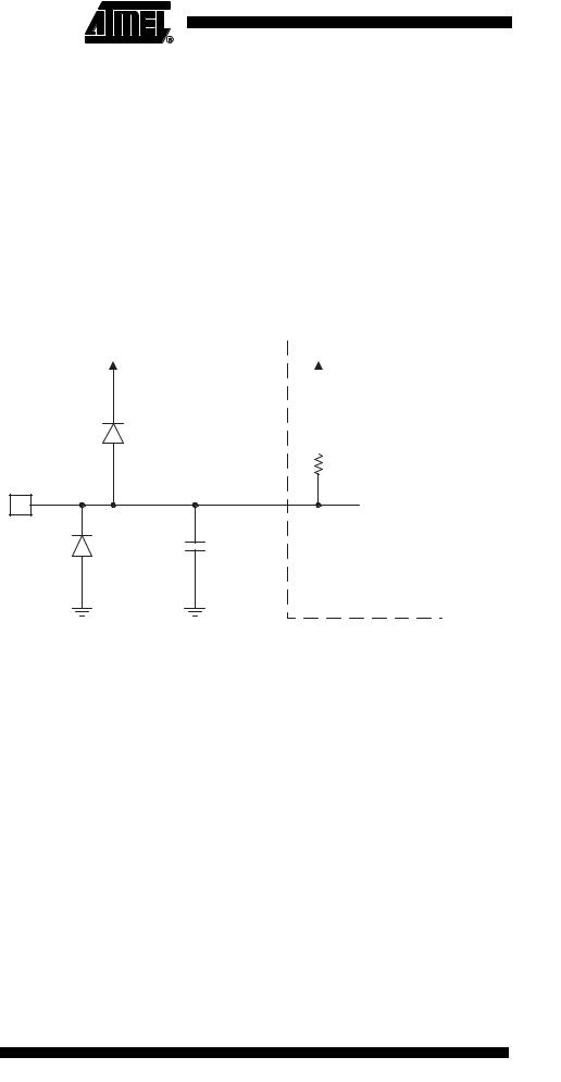
VCC and Ground as indicated in Figure 29. Refer to “Electrical Characteristics” on page |
||||
|
195 for a complete list of parameters. |
||||
|
Figure 29. I/O Pin Equivalent Schematic |
||||
|
|
|
|
|
|
|
|
|
|
|
|
|
|
|
|
|
|
|
|
|
|
|
|
|
|
|
|
|
|
|
Rpu |
Pxn |
Logic |
Cpin |
See Figure |
|
"General Digital I/O" for |
|
Details |
All registers and bit references in this section are written in general form. A lower case “x” represents the numbering letter for the port, and a lower case “n” represents the bit number. However, when using the register or bit defines in a program, the precise form must be used. For example, PORTB3 for bit no. 3 in Port B, here documented generally as PORTxn. The physical I/O Registers and bit locations are listed in “Register Description for I/O Ports” on page 74.
Three I/O memory address locations are allocated for each port, one each for the Data Register – PORTx, Data Direction Register – DDRx, and the Port Input Pins – PINx. The Port Input Pins I/O location is read only, while the Data Register and the Data Direction Register are read/write. In addition, the Pull-up Disable – PUD bit in SFIOR disables the pull-up function for all pins in all ports when set.
Using the I/O port as General Digital I/O is described in “Ports as General Digital I/O” on page 59. Most port pins are multiplexed with alternate functions for the peripheral features on the device. How each alternate function interferes with the port pin is described in “Alternate Port Functions” on page 63. Refer to the individual module sections for a full description of the alternate functions.
Note that enabling the alternate function of some of the port pins does not affect the use of the other pins in the port as general digital I/O.
58 ATmega8515(L)
2512G–AVR–03/05

 ATmega8515(L)
Ports as General Digital
I/O
The ports are bi-directional I/O ports with optional internal pull-ups. Figure 30 shows a functional description of one I/O-port pin, here generically called Pxn.
Figure 30. General Digital I/O(1)
|
|
|
|
|
|
PUD |
|
|
|
|
|
Q |
D |
|
|
|
|
|
|
DDxn |
|
|
|
|
|
|
|
Q CLR |
|
|
|
|
|
|
|
RESET |
WDx |
|
|
|
|
|
|
|
|
||
|
|
|
|
|
|
RDx |
|
Pxn |
|
|
|
Q |
D |
|
BUS |
|
|
|
|
DATA |
|||
|
|
|
|
PORTxn |
|
||
|
|
|
|
|
|
||
|
|
|
|
Q CLR |
|
|
|
|
|
|
|
RESET |
WPx |
|
|
|
|
|
|
|
|
||
|
|
SLEEP |
|
|
|
RRx |
|
|
|
SYNCHRONIZER |
|
RPx |
|
||
|
|
|
|
|
|
|
|
|
|
D |
Q |
D Q |
|
|
|
|
|
|
|
PINxn |
|
|
|
|
|
L |
Q |
Q |
|
|
|
|
|
|
|
|
|
clk I/O |
|
PUD: |
PULLUP DISABLE |
WDx: |
WRITE DDRx |
|
|
|
|
RDx: |
READ DDRx |
|
|
|
|||
SLEEP: |
SLEEP CONTROL |
WPx: |
WRITE PORTx |
|
|
||
clkI/O: |
I/O CLOCK |
RRx: |
READ PORTx REGISTER |
|
|
||
|
|
RPx: |
READ PORTx PIN |
|
|
||
|
Note: 1. WPx, WDx, RRx, RPx, and RDx are common to all pins within the same port. clkI/O, |
||||
|
SLEEP, and PUD are common to all ports. |
||||
Configuring the Pin |
Each port pin consists of three register bits: DDxn, PORTxn, and PINxn. As shown in |
||||
|
“Register Description for I/O Ports” on page 74, the DDxn bits are accessed at the DDRx |
||||
|
I/O address, the PORTxn bits at the PORTx I/O address, and the PINxn bits at the PINx |
||||
|
I/O address. |
||||
|
The DDxn bit in the DDRx Register selects the direction of this pin. If DDxn is written |
||||
|
logic one, Pxn is configured as an output pin. If DDxn is written logic zero, Pxn is config- |
||||
|
ured as an input pin. |
||||
|
If PORTxn is written a logic one when the pin is configured as an input pin, the pull-up |
||||
|
resistor is activated. To switch the pull-up resistor off, PORTxn has to be written a logic |
||||
|
zero or the pin has to be configured as an output pin. The port pins are tri-stated when a |
||||
|
reset condition becomes active, even if no clocks are running. |
||||
|
If PORTxn is written a logic one when the pin is configured as an output pin, the port pin |
||||
|
is driven high (one). If PORTxn is written a logic zero when the pin is configured as an |
||||
|
output pin, the port pin is driven low (zero). |
||||
|
When switching between tri-state ({DDxn, PORTxn} = 0b00) and output high ({DDxn, |
||||
|
PORTxn} = 0b11), an intermediate state with either pull-up enabled ({DDxn, PORTxn} = |
||||
|
0b01) or output low ({DDxn, PORTxn} = 0b10) must occur. Normally, the pull-up |
||||
|
|
|
|
|
|
|
|
|
|
|
59 |
2512G–AVR–03/05 |
|
|
|
|
|
|
|
|
|
|
|
enabled state is fully acceptable, as a high-impedant environment will not notice the difference between a strong high driver and a pull-up. If this is not the case, the PUD bit in the SFIOR Register can be set to disable all pull-ups in all ports.
Switching between input with pull-up and output low generates the same problem. The user must use either the tri-state ({DDxn, PORTxn} = 0b00) or the output high state ({DDxn, PORTxn} = 0b11) as an intermediate step.
Table 24 summarizes the control signals for the pin value.
Table 24. Port Pin Configurations
|
|
PUD |
|
|
|
DDxn |
PORTxn |
(in SFIOR) |
I/O |
Pull-up |
Comment |
|
|
|
|
|
|
0 |
0 |
X |
Input |
No |
Tri-state (Hi-Z) |
|
|
|
|
|
|
|
|
|
|
|
Pxn will source current if ext. pulled |
0 |
1 |
0 |
Input |
Yes |
low. |
|
|
|
|
|
|
0 |
1 |
1 |
Input |
No |
Tri-state (Hi-Z) |
|
|
|
|
|
|
1 |
0 |
X |
Output |
No |
Output Low (Sink) |
|
|
|
|
|
|
1 |
1 |
X |
Output |
No |
Output High (Source) |
|
|
|
|
|
|
Reading the Pin Value |
Independent of the setting of Data Direction bit DDxn, the port pin can be read through |
|
the PINxn Register bit. As shown in Figure 30, the PINxn Register bit and the preceding |
|
latch constitute a synchronizer. This is needed to avoid metastability if the physical pin |
|
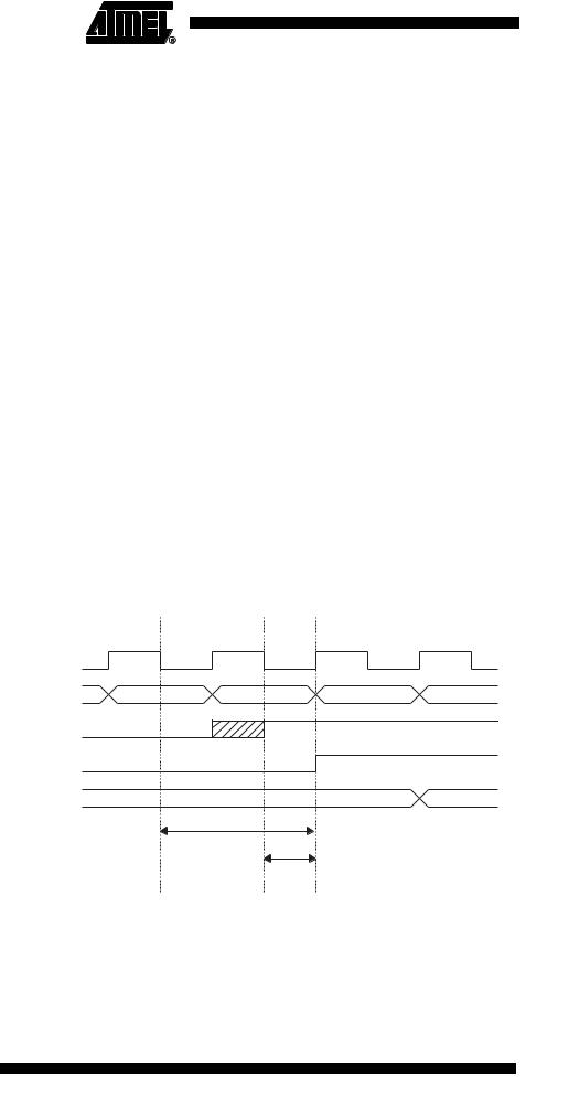
changes value near the edge of the internal clock, but it also introduces a delay. Figure |
|
31 shows a timing diagram of the synchronization when reading an externally applied |
|
pin value. The maximum and minimum propagation delays are denoted tpd,max and tpd,min |
|
respectively. |
|
Figure 31. Synchronization when Reading an Externally Applied Pin Value |
SYSTEM CLK
INSTRUCTIONS
SYNC LATCH
PINxn
r17
XXX |
XXX |
in r17, PINx |
0x00 |
0xFF |
tpd, max
tpd, min
Consider the clock period starting shortly after the first falling edge of the system clock. The latch is closed when the clock is low, and goes transparent when the clock is high, as indicated by the shaded region of the “SYNC LATCH” signal. The signal value is latched when the system clock goes low. It is clocked into the PINxn Register at the succeeding positive clock edge. As indicated by the two arrows tpd,max and tpd,min, a single
60 ATmega8515(L)
2512G–AVR–03/05
 ATmega8515(L)
signal transition on the pin will be delayed between ½ and 1½ system clock period depending upon the time of assertion.
When reading back a software assigned pin value, a nop instruction must be inserted as indicated in Figure 32. The out instruction sets the “SYNC LATCH” signal at the positive edge of the clock. In this case, the delay tpd through the synchronizer is one system clock period.
Figure 32. Synchronization when Reading a Software Assigned Pin Value
SYSTEM CLK
r16
INSTRUCTIONS
SYNC LATCH
PINxn
r17
0xFF
out PORTx, r16 |
nop |
in r17, PINx |
0x00 |
0xFF |
tpd
61
2512G–AVR–03/05

The following code example shows how to set port B pins 0 and 1 high, 2 and 3 low, and define the port pins from 4 to 7 as input with pull-ups assigned to port pins 6 and 7. The resulting pin values are read back again, but as previously discussed, a nop instruction is included to be able to read back the value recently assigned to some of the pins.
Assembly Code Example(1)
...
;Define pull-ups and set outputs high
;Define directions for port pins
ldi r16,(1<<PB7)|(1<<PB6)|(1<<PB1)|(1<<PB0) ldi r17,(1<<DDB3)|(1<<DDB2)|(1<<DDB1)|(1<<DDB0) out PORTB,r16
out DDRB,r17
; Insert nop for synchronization
nop
; Read port pins in r16,PINB
...
C Code Example
unsigned char i;
...
/* Define pull-ups and set outputs high */ /* Define directions for port pins */
PORTB = (1<<PB7)|(1<<PB6)|(1<<PB1)|(1<<PB0); DDRB = (1<<DDB3)|(1<<DDB2)|(1<<DDB1)|(1<<DDB0); /* Insert nop for synchronization*/
_NOP();
/* Read port pins */ i = PINB;
...
Note: 1. For the assembly program, two temporary registers are used to minimize the time from pull-ups are set on pins 0, 1, 6, and 7, until the direction bits are correctly set, defining bit 2 and 3 as low and redefining bits 0 and 1 as strong high drivers.
Digital Input Enable and Sleep As shown in Figure 30, the digital input signal can be clamped to ground at the input of Modes the Schmitt Trigger. The signal denoted SLEEP in the figure, is set by the MCU Sleep Controller in Power-down mode and Standby mode to avoid high power consumption if
some input signals are left floating, or have an analog signal level close to VCC/2.
SLEEP is overridden for port pins enabled as External Interrupt pins. If the External Interrupt Request is not enabled, SLEEP is active also for these pins. SLEEP is also overridden by various other alternate functions as described in “Alternate Port Functions” on page 63.
If a logic high level (“one”) is present on an Asynchronous External Interrupt pin configured as “Interrupt on Rising Edge, Falling Edge, or Any Logic Change on Pin” while the external interrupt is not enabled, the corresponding External Interrupt Flag will be set when resuming from the above mentioned sleep modes, as the clamping in these sleep modes produces the requested logic change.
62 ATmega8515(L)
2512G–AVR–03/05