

 ATmega8515(L)
8-bit Timer/Counter0 with PWM
Timer/Counter0 is a general purpose, single channel, 8-bit Timer/Counter module. The main features are:
•Single Channel Counter
•Clear Timer on Compare Match (Auto Reload)
•Glitch-free, Phase Correct Pulse Width Modulator (PWM)
•Frequency Generator
•External Event Counter
•10-bit Clock Prescaler
•Overflow and Compare Match Interrupt Sources (TOV0 and OCF0)
Overview |
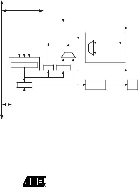
A simplified block diagram of the 8-bit Timer/Counter is shown in Figure 34. For the |
|
actual placement of I/O pins, refer to “Pinout ATmega8515” on page 2. CPU accessible |
|
I/O Registers, including I/O bits and I/O pins, are shown in bold. The device-specific I/O |
|
Register and bit locations are listed in the “8-bit Timer/Counter Register Description” on |
|
page 90. |
|
Figure 34. 8-bit Timer/Counter Block Diagram |
DATA BUS

|
|
|
|
TCCRn |
|
|
|
|
|
|
|
|
|
|
|
|
|
|
||
|
|
|
|
|
|
|
|
|
|
|
|
|
|
|
|
|
|
|
|
|
|
|
|
|
|
|
|
|
|
|
|
|
|
|
|
|
|
|
|
|
|
|
|
|
|
|
|
|
|
|
|
|
|
|
|
|
|
|
|
|
|
|
|
|
count |
|
|
|
|
|
|
|
|
|
|
|
|
|
|
|
|
TOVn |
|
|
|
clear |
|
Control Logic |
|
|
|
|
|
|
|
|
|
|
|
|
(Int.Req.) |
|||
|
|
|
|
|
|
|
|
|
|
|
|
|
|
|
|
|
|
|||
|
|
direction |
|
clkTn |
|
|
|
Clock Select |
|
|
|
|
||||||||
|
|
|
|
|
|
|
|
|
|
|
|
|
||||||||
|
|
|
|
|
|
|
|
|
|
|
|
|
Edge |
|
|
|
Tn |
|
||
|
|
|
|
|
|
|
|
|
|
|
|
|
Detector |
|
|
|
|
|
||
|
|
|
|
|
|
|
|
|
|
|
|
|
|
|
|
|
|
|||
|
|
BOTTOM |
TOP |
|
|
|
|
|
|
|
|
|
|
|
|
|
||||
|
|
|
|
|
|
|
|
|
|
|
|
|
|
|||||||
|
|
|
|
|
|
|
|
|
|
|
|
|
|
|
|
|
|
|
|
|
|
|
|
|
|
|
|
|
|
|
|
|
|
|
|
|
|
|
|
|
|
|
|
|
|
|
|
|
|
|
|
|
|
|
|
|
|
|
|
|
|
|
Timer/Counter |
( From Prescaler ) |
|
|
|
|
||
TCNTn |
= 0xFF |
|
|
= 0 |
OCn |
||
|
|
||
|
|
(Int.Req.) |
|
= |
Waveform |
OCn |
|
Generation |
|||
|
|
|
|
|
|
|
|
|
|
|
|
Registers |
|
|
|
|
OCRn |
|
|||
|
|
|
|
|
|
|
|||
|
|
|
|
|
|
||||
The Timer/Counter (TCNT0) and Output Compare Register (OCR0) are 8-bit registers. |
|||||||||
|
Interrupt request (abbreviated to Int.Req. in the figure) signals are all visible in the Timer |
||||||||
|
Interrupt Flag Register (TIFR). All interrupts are individually masked with the Timer |
||||||||
|
Interrupt Mask Register (TIMSK). TIFR and TIMSK are not shown in the figure since |
||||||||
|
these registers are shared by other timer units. |
||||||||
|
The Timer/Counter can be clocked internally, via the prescaler, or by an external clock |
||||||||
|
source on the T0 pin. The Clock Select logic block controls which clock source and edge |
||||||||
|
the Timer/Counter uses to increment (or decrement) its value. The Timer/Counter is |
||||||||
|
|
|
|
|
|
|
|
|
|
|
|
|
|
|
|
|
|
|
79 |
2512G–AVR–03/05 |
|
|
|
|
|
|
|
|
|
|
|
|
|
|
|
|
|
|
|
|
|
|
|
|
|
|
|
|
|
|
|
|
|
|
inactive when no clock source is selected. The output from the clock select logic is |
|||||
|
referred to as the timer clock (clkT0). |
|||||
|
The double buffered Output Compare Register (OCR0) is compared with the |
|||||
|
Timer/Counter value at all times. The result of the compare can be used by the Wave- |
|||||
|
form Generator to generate a PWM or variable frequency output on the Output Compare |
|||||
|
Pin (OC0). See “Output Compare Unit” on page 81. for details. The Compare Match |
|||||
|
event will also set the Compare Flag (OCF0) which can be used to generate an output |
|||||
|
compare interrupt request. |
|||||
Definitions |
Many register and bit references in this document are written in general form. A lower |
|||||
|
case “n” replaces the Timer/Counter number, in this case 0. However, when using the |
|||||
|
register or bit defines in a program, the precise form must be used, i.e., TCNT0 for |
|||||
|
accessing Timer/Counter0 counter value and so on. |
|||||
|
The definitions in Table 43 are also used extensively throughout the document. |
|||||
|
Table 43. Definitions |
|||||
|
|
|
||||
|
BOTTOM |
The counter reaches the BOTTOM when it becomes 0x00. |
||||
|
MAX |
The counter reaches its MAXimum when it becomes 0xFF (decimal 255). |
||||
|
TOP |
The counter reaches the TOP when it becomes equal to the highest |
||||
|
|
value in the count sequence. The TOP value can be assigned to be the |
||||
|
|
fixed value 0xFF (MAX) or the value stored in the OCR0 Register. The |
||||
|
|
assignment is dependent on the mode of operation. |
||||
|
|
|
|
|
|
|
Timer/Counter Clock
Sources
Counter Unit
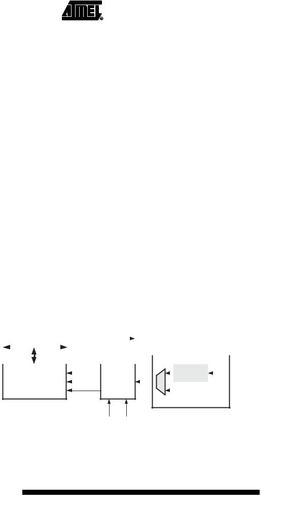
The Timer/Counter can be clocked by an internal or an external clock source. The clock source is selected by the clock select logic which is controlled by the Clock Select (CS02:0) bits located in the Timer/Counter Control Register (TCCR0). For details on clock sources and prescaler, see “Timer/Counter0 and Timer/Counter1 Prescalers” on page 94.
The main part of the 8-bit Timer/Counter is the programmable bi-directional counter unit. Figure 35 shows a block diagram of the counter and its surroundings.
Figure 35. Counter Unit Block Diagram
|
|
|
|
|
|
|
|
|
TOVn |
|
|
|
|
|
|
||||
|
DATA BUS |
|
|
|
|
(Int.Req.) |
|
|
|
|
|
|
|||||||
|
|
|
|
|
|
|
|
|
|
|
|
|
|
|
|
|
|
|
|
|
|
|
|
|
|
|
|
|
|
|
|
|
|
Clock Select |
|
|
|||
|
|
|
|
count |
|
|
|
|
|
|
|
|
|
|
|
|
|
|
|
|
|
|
|
|
|
|
|
|
|
|
|
|
Edge |
|
|
|
Tn |
||
|
TCNTn |
clear |
|
|
|
|
clkTn |
Detector |
|
|
|
||||||||
|
|
|
|
|
|
|
|
||||||||||||
|
|
|
Control Logic |
|
|
|
|
|
|
|
|
||||||||
|
direction |
|
|
|
|
|
|
|
|
|
|||||||||
|
|
|
|
|
|
|
|
|
|
|
|
|
|
|
|
|
|
|
|
|
|
|
|
|
|
|
|
|
|
|
|
|
|
|
|
|
|
|
|
( From Prescaler )
bottom top
Signal description (internal signals):
count Increment or decrement TCNT0 by 1.
direction Select between increment and decrement.
clear Clear TCNT0 (set all bits to zero).
80 ATmega8515(L)
2512G–AVR–03/05