

Features
•High-performance, Low-power AVR® 8-bit Microcontroller
•RISC Architecture
–130 Powerful Instructions – Most Single Clock Cycle Execution
–32 x 8 General Purpose Working Registers
–Fully Static Operation
–Up to 16 MIPS Throughput at 16 MHz
–On-chip 2-cycle Multiplier
•Nonvolatile Program and Data Memories
–8K Bytes of In-System Self-programmable Flash
Endurance: 10,000 Write/Erase Cycles
–Optional Boot Code Section with Independent Lock bits In-System Programming by On-chip Boot Program True Read-While-Write Operation
–512 Bytes EEPROM
Endurance: 100,000 Write/Erase Cycles
–512 Bytes Internal SRAM
–Up to 64K Bytes Optional External Memory Space
–Programming Lock for Software Security
•Peripheral Features
–One 8-bit Timer/Counter with Separate Prescaler and Compare Mode
–One 16-bit Timer/Counter with Separate Prescaler, Compare Mode, and Capture Mode
–Three PWM Channels
–Programmable Serial USART
–Master/Slave SPI Serial Interface
–Programmable Watchdog Timer with Separate On-chip Oscillator
–On-chip Analog Comparator
•Special Microcontroller Features
–Power-on Reset and Programmable Brown-out Detection
–Internal Calibrated RC Oscillator
–External and Internal Interrupt Sources
–Three Sleep Modes: Idle, Power-down and Standby
•I/O and Packages
–35 Programmable I/O Lines
–40-pin PDIP, 44-lead TQFP, 44-lead PLCC, and 44-pad QFN/MLF
•Operating Voltages
–2.7 - 5.5V for ATmega8515L
–4.5 - 5.5V for ATmega8515
•Speed Grades
–0 - 8 MHz for ATmega8515L
–0 - 16 MHz for ATmega8515
8-bit  Microcontroller with 8K Bytes In-System Programmable Flash
ATmega8515
ATmega8515L
Rev. 2512G–AVR–03/05
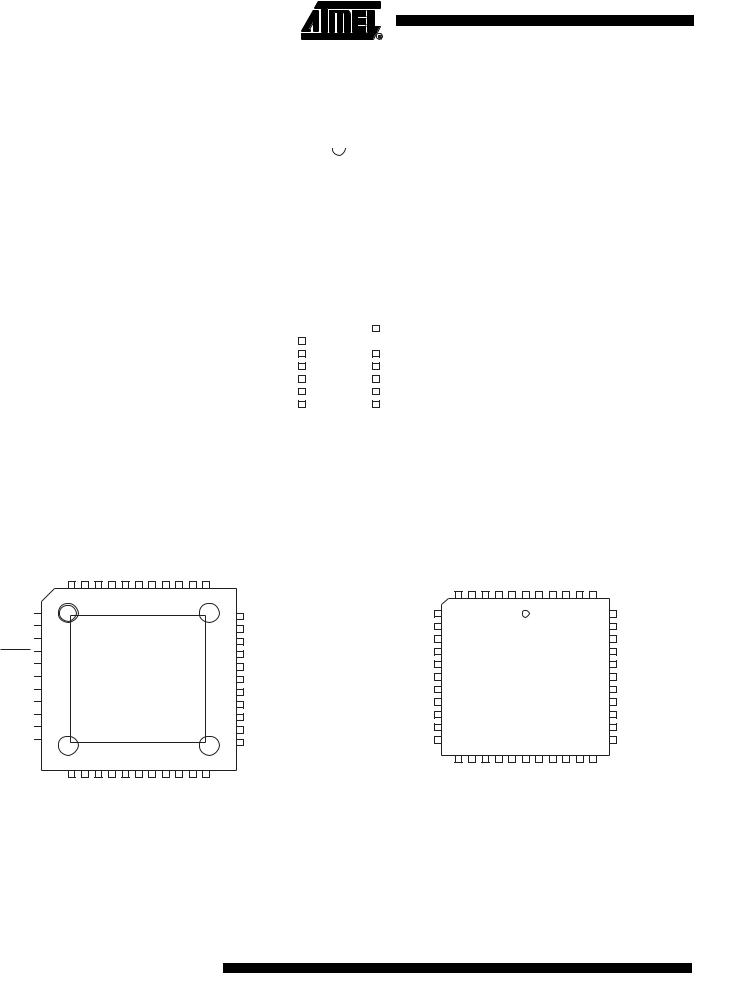
Pin Configurations
Figure 1. Pinout ATmega8515
(MOSI) PB5 
 1 (MISO) PB6
 2 (SCK) PB7
  3 RESET
 4 (RXD) PD0
  5 NC*
5 NC* 
 6 (TXD) PD1
  7
7
(INT0) PD2 
 8 (INT1) PD3
 9 (XCK) PD4
  10 (OC1A) PD5
  11
11
PDIP
(OC0/T0) PB0 |
|
1 |
40 |
|
VCC |
|||||
|
|
|||||||||
|
|
(T1) PB1 |
|
2 |
39 |
|
PA0 (AD0) |
|||
|
|
|||||||||
(AIN0) PB2 |
|
3 |
38 |
|
PA1 (AD1) |
|||||
|
|
|||||||||
(AIN1) PB3 |
|
4 |
37 |
|
PA2 (AD2) |
|||||
|
|
|||||||||
|
(SS) PB4 |
|
5 |
36 |
|
PA3 (AD3) |
||||
|
|
|||||||||
(MOSI) PB5 |
|
6 |
35 |
|
PA4 (AD4) |
|||||
|
|
|||||||||
(MISO) PB6 |
|
7 |
34 |
|
PA5 (AD5) |
|||||
|
|
|||||||||
(SCK) PB7 |
|
8 |
33 |
|
PA6 (AD6) |
|||||
|
|
|||||||||
|
|
|
|
|
9 |
32 |
|
PA7 (AD7) |
||
|
|
|
RESET |
|
|
|
||||
|
|
|||||||||
(RXD) PD0 |
|
10 |
31 |
|
PE0 (ICP/INT2) |
|||||
|
|
|||||||||
(TDX) PD1 |
|
11 |
30 |
|
PE1 (ALE) |
|||||
|
|
|||||||||
(INT0) PD2 |
|
12 |
29 |
|
PE2 (OC1B) |
|||||
|
|
|||||||||
(INT1) PD3 |
|
13 |
28 |
|
PC7 (A15) |
|||||
|
|
|||||||||
(XCK) PD4 |
|
14 |
27 |
|
PC6 (A14) |
|||||
|
|
|||||||||
(OC1A) PD5 |
|
15 |
26 |
|
PC5 (A13) |
|||||
|
||||||||||
|
|
|
|
|
|
|
|
|
||
(WR) PD6 |
|
16 |
25 |
|
PC4 (A12) |
|||||
|
|
17 |
24 |
|
PC3 (A11) |
|||||
|
(RD) |
PD7 |
|
|
||||||
|
|
|
XTAL2 |
|
18 |
23 |
|
PC2 (A10) |
||
|
|
|
XTAL1 |
|
19 |
22 |
|
PC1 (A9) |
||
|
|
|
|
GND |
|
20 |
21 |
|
PC0 (A8) |
|
|
|
|
|
|
|
|
|
|
|
|
|
|
|
|
|
TQFP/MLF |
|
|
|
|
|
|
|
|
|
|
|
|
PLCC |
|
|
|
|
|
||||||
|
PB4 (SS) |
|
PB3 (AIN1) |
PB2 (AIN0) |
PB1 (T1) |
PB0 (OC0/T0) |
NC* |
VCC |
PA0 (AD0) |
PA1 (AD1) |
PA2 (AD2) |
PA3 (AD3) |
|
|
|
|
PB4 (SS) |
|
PB3 (AIN1) |
PB2 (AIN0) |
PB1 (T1) |
PB0 (OC0/T0) |
NC* |
VCC |
PA0 (AD0) |
PA1 (AD1) |
PA2 (AD2) |
PA3 (AD3) |
|
44 |
43 |
42 |
41 |
40 |
39 |
38 |
37 |
36 |
35 |
34 |
|
|
|
6 |
5 |
4 |
3 |
2 |
1 |
44 |
43 |
42 |
41 |
40 |
|
||||
|
|
|
|
|
|
|
|
|
|
|
|
|
|
(MOSI) PB5 |
PA4 (AD4) |
||||||||||||||
|
|
|
|
|
|
|
|
|
|
|
|
33 |
PA4 (AD4) |
7 |
|
|
|
|
|
|
|
|
|
|
|
39 |
|||
|
|
|
|
|
|
|
|
|
|
|
|
|
|
|
|
|
|
|
|
|
|
|
|
|
|
|
|
||
|
|
|
|
|
|
|
|
|
|
|
|
32 |
PA5 (AD5) |
(MISO) PB6 |
8 |
|
|
|
|
|
|
|
|
|
|
|
38 |
PA5 (AD5) |
|
|
|
|
|
|
|
|
|
|
|
|
|
|
|
|
|
|
|
|
|
|
|
|
|
|
|
|
|
||
|
|
|
|
|
|
|
|
|
|
|
|
31 |
PA6 (AD6) |
(SCK) PB7 |
9 |
|
|
|
|
|
|
|
|
|
|
|
37 |
PA6 (AD6) |
|
|
|
|
|
|
|
|
|
|
|
|
|
30 |
PA7 (AD7) |
|
RESET |
10 |
|
|
|
|
|
|
|
|
|
|
36 |
PA7 (AD7) |
|
|
|
|
|
|
|
|
|
|
|
|
|
|
|
|
|
|
|
|
|
|
|
|
|
|
|
|
|
||
|
|
|
|
|
|
|
|
|
|
|
|
29 |
PE0 (ICP/INT2) |
(RXD) PD0 |
11 |
|
|
|
|
|
|
|
|
|
|
35 |
PE0 (ICP/INT2) |
||
|
|
|
|
|
|
|
|
|
|
|
|
|
|
|
|
|
|
|
|
|
|
|
|
|
|
|
|
||
|
|
|
|
|
|
|
|
|
|
|
|
28 |
NC* |
|
NC* |
12 |
|
|
|
|
|
|
|
|
|
|
34 |
NC* |
|
|
|
|
|
|
|
|
|
|
|
|
|
|
|
|
|
|
|
|
|
|
|
|
|
|
|
|
|
||
|
|
|
|
|
|
|
|
|
|
|
|
27 |
PE1 (ALE) |
(TXD) PD1 |
13 |
|
|
|
|
|
|
|
|
|
|
33 |
PE1 (ALE) |
||
|
|
|
|
|
|
|
|
|
|
|
|
|
|
|
|
|
|
|
|
|
|
|
|
|
|
|
|
||
|
|
|
|
|
|
|
|
|
|
|
|
26 |
PE2 (OC1B) |
(INT0) PD2 |
14 |
|
|
|
|
|
|
|
|
|
|
32 |
PE2 (OC1B) |
||
|
|
|
|
|
|
|
|
|
|
|
|
|
|
|
|
|
|
|
|
|
|
|
|
|
|
|
|
||
|
|
|
|
|
|
|
|
|
|
|
|
25 |
PC7 (A15) |
(INT1) PD3 |
15 |
|
|
|
|
|
|
|
|
|
|
31 |
PC7 (A15) |
||
|
|
|
|
|
|
|
|
|
|
|
|
|
|
|
|
|
|
|
|
|
|
|
|
|
|
|
|
||
|
|
|
|
|
|
|
|
|
|
|
|
24 |
PC6 (A14) |
(XCK) PD4 |
16 |
|
|
|
|
|
|
|
|
|
|
30 |
PC6 (A14) |
||
|
|
|
|
|
|
|
|
|
|
|
|
|
|
|
|
|
|
|
|
|
|
|
|
|
|
|
|
||
|
|
|
|
|
|
|
|
|
|
|
|
23 |
PC5 (A13) |
(OC1A) PD5 |
17 |
|
|
|
|
|
|
|
|
|
|
29 |
PC5 (A13) |
||
|
|
|
|
|
|
|
|
|
|
|
|
|
|
18 |
19 |
20 |
21 |
22 |
23 |
24 |
25 |
26 |
27 |
28 |
|
||||
|
|
|
|
|
|
|
|
|
|
|
|
|
|
|
|
|
|||||||||||||
|
(WR) PD6 12 |
|
(RD) PD7 13 |
XTAL2 14 |
XTAL1 15 |
GND 16 |
NC* 17 |
(A8) PC0 18 |
(A9) PC1 19 |
(A10) PC2 20 |
(A11) PC3 21 |
(A12) PC4 22 |
|
|
|
|
(WR) PD6 |
|
(RD) PD7 |
XTAL2 |
XTAL1 |
GND |
NC* |
(A8) PC0 |
(A9) PC1 |
(A10) PC2 |
(A11) PC3 |
(A12) PC4 |
|
|
|
|
|
|
|
|
|
|
|
||||||||||||||||||||
|
|
|
|
|
|
|
|
|
|
|
|
||||||||||||||||||
|
|
|
|
|
|
|
|
|
|
|
|
|
|
|
|
||||||||||||||
|
|
|
|
|
|
|
|
|
|
|
|
|
|
|
|
|
|
|
|
|
|
|
|
|
|||||
NOTES:
1.MLF bottom pad should be soldered to ground.
2.* NC = Do not connect (May be used in future devices)
2 ATmega8515(L)
2512G–AVR–03/05