

- •Features
- •Pin Configurations
- •Overview
- •Block Diagram
- •Disclaimer
- •Pin Descriptions
- •Port A (PA7..PA0)
- •Port B (PB7..PB0)
- •Port C (PC7..PC0)
- •Port D (PD7..PD0)
- •Port E(PE2..PE0)
- •RESET
- •XTAL1
- •XTAL2
- •AVR CPU Core
- •Introduction
- •Architectural Overview
- •Status Register
- •Stack Pointer
- •Interrupt Response Time
- •In-System Reprogrammable Flash Program memory
- •SRAM Data Memory
- •Data Memory Access Times
- •EEPROM Data Memory
- •EEPROM Read/Write Access
- •I/O Memory
- •Overview
- •Address Latch Requirements
- •Pull-up and Bus Keeper
- •Timing
- •Using all Locations of External Memory Smaller than 64 KB
- •Using all 64KB Locations of External Memory
- •Clock Systems and their Distribution
- •Clock Sources
- •Default Clock Source
- •Crystal Oscillator
- •External RC Oscillator
- •External Clock
- •Idle Mode
- •Power-down Mode
- •Standby Mode
- •Analog Comparator
- •Brown-out Detector
- •Internal Voltage Reference
- •Watchdog Timer
- •Port Pins
- •Resetting the AVR
- •Reset Sources
- •Power-on Reset
- •External Reset
- •Brown-out Detection
- •Watchdog Reset
- •Watchdog Timer
- •Timed Sequences for Changing the Configuration of the Watchdog Timer
- •Safety Level 0
- •Safety Level 1
- •Safety Level 2
- •Interrupts
- •Moving Interrupts between Application and Boot Space
- •I/O Ports
- •Introduction
- •Configuring the Pin
- •Reading the Pin Value
- •Unconnected pins
- •Alternate Port Functions
- •Alternate Functions of Port A
- •Alternate Functions Of Port B
- •Alternate Functions of Port C
- •Alternate Functions of Port D
- •Alternate Functions of Port E
- •Register Description for I/O Ports
- •External Interrupts
- •8-bit Timer/Counter0 with PWM
- •Overview
- •Registers
- •Definitions
- •Counter Unit
- •Output Compare Unit
- •Force Output Compare
- •Modes of Operation
- •Normal Mode
- •Fast PWM Mode
- •Phase Correct PWM Mode
- •Internal Clock Source
- •Prescaler Reset
- •External Clock Source
- •16-bit Timer/Counter1
- •Overview
- •Registers
- •Definitions
- •Compatibility
- •Counter Unit
- •Input Capture Unit
- •Input Capture Trigger Source
- •Noise Canceler
- •Using the Input Capture Unit
- •Output Compare Units
- •Force Output Compare
- •Modes of Operation
- •Normal Mode
- •Fast PWM Mode
- •Phase Correct PWM Mode
- •Slave Mode
- •Master Mode
- •Data Modes
- •USART
- •Single USART
- •Clock Generation
- •External Clock
- •Synchronous Clock Operation
- •Frame Formats
- •Parity Bit Calculation
- •USART Initialization
- •Sending Frames with 5 to 8 Data Bits
- •Sending Frames with 9 Data Bits
- •Parity Generator
- •Disabling the Transmitter
- •Receiving Frames with 5 to 8 Data Bits
- •Receiving Frames with 9 Data Bits
- •Receiver Error Flags
- •Parity Checker
- •Disabling the Receiver
- •Flushing the Receive Buffer
- •Asynchronous Data Recovery
- •Using MPCM
- •Write Access
- •Read Access
- •Analog Comparator
- •Features
- •Application Section
- •Boot Loader Lock bits
- •Performing a Page Write
- •Using the SPM Interrupt
- •Setting the Boot Loader Lock bits by SPM
- •Reading the Fuse and Lock bits from Software
- •Preventing Flash Corruption
- •Simple Assembly Code Example for a Boot Loader
- •Program and Data Memory Lock bits
- •Fuse bits
- •Latching of Fuses
- •Signature Bytes
- •Calibration Byte
- •Calibration Byte
- •Signal Names
- •Parallel Programming
- •Enter Programming Mode
- •Chip Erase
- •Programming the Flash
- •Programming the EEPROM
- •Reading the Flash
- •Reading the EEPROM
- •Programming the Lock bits
- •Reading the Signature Bytes
- •Reading the Calibration Byte
- •Serial Downloading
- •Data Polling Flash
- •Data Polling EEPROM
- •Electrical Characteristics
- •Absolute Maximum Ratings*
- •External Clock Drive Waveforms
- •External Clock Drive
- •External Data Memory Timing
- •Active Supply Current
- •Idle Supply Current
- •Standby Supply Current
- •Pin Pull-up
- •Pin Driver Strength
- •Internal Oscillator Speed
- •Register Summary
- •Instruction Set Summary
- •Ordering Information
- •Packaging Information
- •Errata
- •ATmega8515(L) Rev. B
- •Changes from Rev. 2512F-12/03 to Rev. 2512G-03/05
- •Changes from Rev. 2512F-12/03 to Rev. 2512E-09/03
- •Changes from Rev. 2512D-02/03 to Rev. 2512E-09/03
- •Changes from Rev. 2512C-10/02 to Rev. 2512D-02/03
- •Changes from Rev. 2512B-09/02 to Rev. 2512C-10/02
- •Changes from Rev. 2512A-04/02 to Rev. 2512B-09/02
- •Table of Contents
 ATmega8515(L)
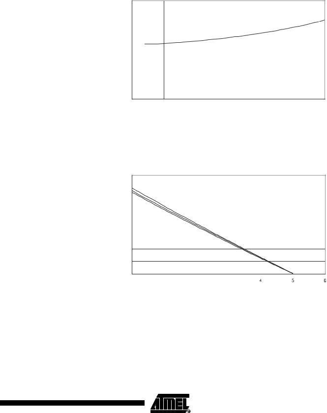
Figure 116. Standby Supply Current vs. VCC (6 MHz XTAL, Watchdog Timer Disabled)
STANDBY SUPPLY CURRENT vs. VCC
6 MHz XTAL, WATCHDOG TIMER DISABLED
|
200 |
|
|
|
|
|
|
|
180 |
|
|
|
|
|
|
|
160 |
|
|
|
|
|
|
|
140 |
|
|
|
|
|
|
(uA) |
120 |
|
|
|
|
|
|
100 |
|
|
|
|
|
|
|
CC |
|
|
|
|
|
|
|
|
|
|
|
|
|
|
|
I |
80 |
|
|
|
|
|
|
|
|
|
|
|
|
|
|
|
60 |
|
|
|
|
|
|
|
40 |
|
|
|
|
|
|
|
20 |
|
|
|
|
|
|
|
0 |
|
|
|
|
|
|
|
2.5 |
3 |
3.5 |
4 |
4.5 |
5 |
5.5 |
VCC (V)
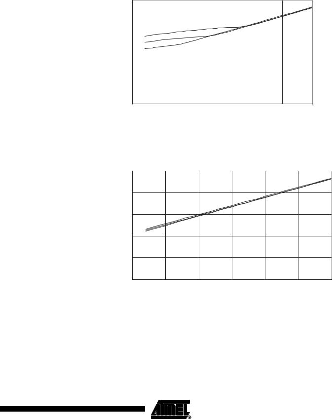
Pin Pull-up |
Figure 117. I/O Pin Pull-up Resistor Current vs. Input Voltage (VCC = 5V) |
I/O PIN PULL-UP RESISTOR CURRENT vs. INPUT VOLTAGE
|
|
|
|
Vcc = 5 V |
|
160 |
|
|
|
85°C |
|
|
|
|
|
140 |
|
|
|
|
|
25°C |
|
|
|
120 |
|
|
|
|
|
-40°C |
|
|
|
100 |
|
|
|
(uA) |
80 |
|
|
|
OP |
|
|
|
|
|
|
|
|
|
I |
|
|
|
|
|
60 |
|
|
|
|
40 |
|
|
|
|
20 |
|
|
|
|
0 |
|
|
|
|
0 |
1 |
2 |
3 |
VOP (V)
217
2512G–AVR–03/05
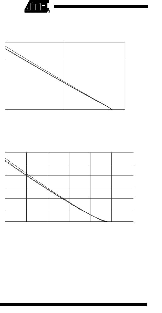
Figure 118. I/O Pin Pull-up Resistor Current vs. Input Voltage (VCC = 2.7V)
I/O PIN PULL-UP RESISTOR CURRENT vs. INPUT VOLTAGE
|
|
|
|
Vcc = 2,7 V |
|
|
|
|
80 |
|
|
|
|
|
|
85°C |
25°C |
|
|
|
|
|
|
|
70 |
|
|
|
|
|
|
|
-40°C |
|
|
|
|
|
|
|
60 |
|
|
|
|
|
|
|
50 |
|
|
|
|
|
|
(uA) |
40 |
|
|
|
|
|
|
OP |
|
|
|
|
|
|
|
|
|
|
|
|
|
|
|
I |
|
|
|
|
|
|
|
|
30 |
|
|
|
|
|
|
|
20 |
|
|
|
|
|
|
|
10 |
|
|
|
|
|
|
|
0 |
|
|
|
|
|
|
|
0 |
0.5 |
1 |
1.5 |
2 |
2.5 |
3 |
VOP (V)
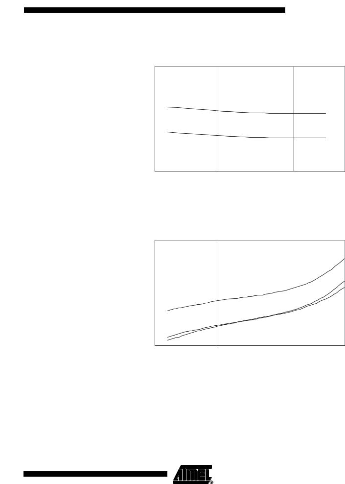
Figure 119. Reset Pull-up Resistor Current vs. Reset Pin Voltage (VCC = 5V)
RESET PULL-UP RESISTOR CURRENT vs. RESET PIN VOLTAGE
|
|
|
|
Vcc = 5V |
|
|
|
|
120 |
|
|
|
|
|
|
-40°C |
25°C |
|
|
|
|
|
|
|
|
|
|
|
|
|
|
|
100 |
|
|
|
|
|
|
|
80 |
85°C |
|
|
|
|
|
|
|
|
|
|
|
|
|
(uA) |
60 |
|
|
|
|
|
|
RESET |
|
|
|
|
|
|
|
|
|
|
|
|
|
|
|
I |
|
|
|
|
|
|
|
|
40 |
|
|
|
|
|
|
|
20 |
|
|
|
|
|
|
|
0 |
|
|
|
|
|
|
|
0 |
1 |
2 |
3 |
4 |
5 |
6 |
VRESET (V)
218 ATmega8515(L)
2512G–AVR–03/05
 ATmega8515(L)
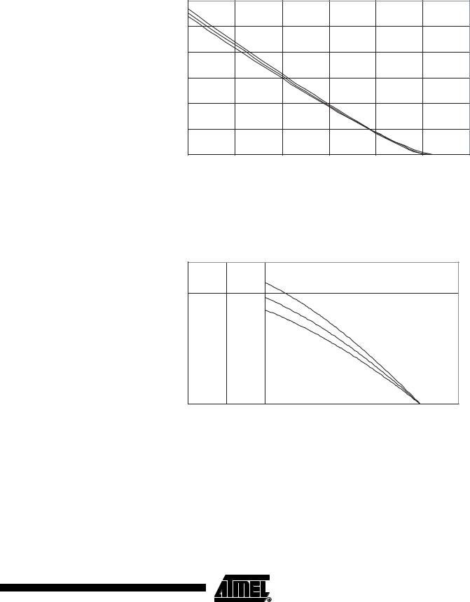
Figure 120. Reset Pull-up Resistor Current vs. Reset Pin Voltage (VCC = 2.7V)
RESET PULL-UP RESISTOR CURRENT vs. RESET PIN VOLTAGE
|
|
|
|
Vcc = 2.7V |
|
|
|
|
60 |
|
|
|
|
|
|
-40°C |
25°C |
|
|
|
|
|
|
|
50 |
|
|
|
|
|
|
|
|
85°C |
|
|
|
|
|
|
40 |
|
|
|
|
|
|
(uA) |
30 |
|
|
|
|
|
|
RESET |
|
|
|
|
|
|
|
|
|
|
|
|
|
|
|
I |
|
|
|
|
|
|
|
|
20 |
|
|
|
|
|
|
|
10 |
|
|
|
|
|
|
|
0 |
|
|
|
|
|
|
|
0 |
0.5 |
1 |
1.5 |
2 |
2.5 |
3 |
VRESET (V)
Pin Driver Strength |
Figure 121. I/O Pin Source Current vs. Output Voltage (VCC = 5V) |
|
I/O PIN SOURCE CURRENT vs. OUTPUT VOLTAGE |
|
Vcc = 5 V |
IOH (mA)
90
80
-40°C
70
25°C
60
85°C
50
40
30
20
10
0
2 |
2.5 |
3 |
3.5 |
4 |
4.5 |
5 |
5.5 |
VOH (V)
219
2512G–AVR–03/05
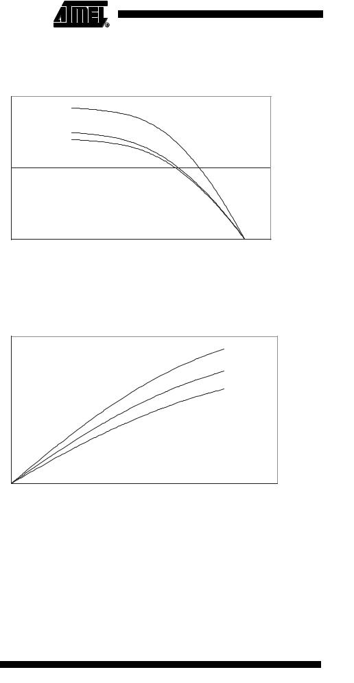
Figure 122. I/O Pin Source Current vs. Output Voltage (VCC = 2.7V)
I/O PIN SOURCE CURRENT vs. OUTPUT VOLTAGE
Vcc = 2,7 V
IOH (mA)
30
-40°C
25
85°C
25°C
20
15
10
5
0
0 |
0.5 |
1 |
1.5 |
2 |
2.5 |
3 |
VOH (V)
Figure 123. I/O Pin Sink Current vs. Output Voltage (VCC = 5V)
I/O PIN SINK CURRENT vs. OUTPUT VOLTAGE
|
|
|
|
Vcc = 5 V |
|
|
|
90 |
|
|
|
|
|
|
|
|
|
|
|
-40°C |
|
80 |
|
|
|
|
|
|
70 |
|
|
|
|
|
|
|
|
|
|
|
25°C |
|
60 |
|
|
|
|
|
|
|
|
|
|
|
85°C |
(mA) |
50 |
|
|
|
|
|
|
|
|
|
|
|
|
OL |
40 |
|
|
|
|
|
I |
|
|
|
|
|
|
|
30 |
|
|
|
|
|
|
20 |
|
|
|
|
|
|
10 |
|
|
|
|
|
|
0 |
|
|
|
|
|
|
0 |
0.5 |
1 |
1.5 |
2 |
2.5 |
VOL (V)
220 ATmega8515(L)
2512G–AVR–03/05
 ATmega8515(L)
Pin Thresholds And
Hysteresis
Figure 124. I/O Pin Sink Current vs. Output Voltage (VCC = 2.7V)
I/O PIN SINK CURRENT vs. OUTPUT VOLTAGE
|
|
|
|
Vcc = 2,7 V |
|
|
|
35 |
|
|
|
|
|
|
|
|
|
|
|
-40°C |
|
30 |
|
|
|
|
|
|
25 |
|
|
|
|
25°C |
|
|
|
|
|
|
|
|
|
|
|
|
|
85°C |
(mA) |
20 |
|
|
|
|
|
|
|
|
|
|
|
|
OL |
15 |
|
|
|
|
|
I |
|
|
|
|
|
|
|
|
|
|
|
|
|
|
10 |
|
|
|
|
|
|
5 |
|
|
|
|
|
|
0 |
|
|
|
|
|
|
0 |
0.5 |
1 |
1.5 |
2 |
2.5 |
VOL (V)
Figure 125. I/O Pin Input Threshold Voltage vs. VCC (VIH, I/O Pin Read As '1')
I/O PIN INPUT THRESHOLD VOLTAGE vs. VCC
VIH, IO PIN READ AS '1'
|
2.5 |
|
|
|
|
|
|
|
|
|
|
|
|
|
-40°C |
|
2 |
|
|
|
|
|
85°C |
|
|
|
|
|
|
|
25°C |
Threshold (V) |
1.5 |
|
|
|
|
|
|
1 |
|
|
|
|
|
|
|
|
0.5 |
|
|
|
|
|
|
|
0 |
|
|
|
|
|
|
|
2.5 |
3 |
3.5 |
4 |
4.5 |
5 |
5.5 |
VCC (V)
221
2512G–AVR–03/05
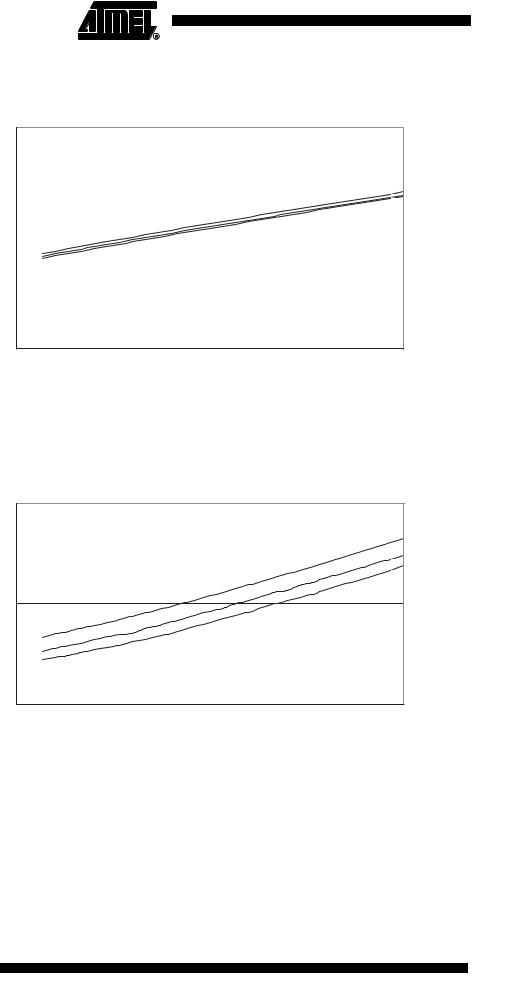
Figure 126. I/O Pin Input Threshold Voltage vs. VCC (VIL, I/O Pin Read As '0')
I/O PIN INPUT THRESHOLD VOLTAGE vs. VCC
VIL, IO PIN READ AS '0'
|
2.5 |
|
|
|
|
|
|
|
2 |
|
|
|
|
|
-40°C |
|
|
|
|
|
|
|
|
|
|
|
|
|
|
|
25°C |
|
|
|
|
|
|
|
85°C |
Threshold (V) |
1.5 |
|
|
|
|
|
|
1 |
|
|
|
|
|
|
|
|
0.5 |
|
|
|
|
|
|
|
0 |
|
|
|
|
|
|
|
2.5 |
3 |
3.5 |
4 |
4.5 |
5 |
5.5 |
VCC (V)
Figure 127. I/O Pin Input Hysteresis vs. VCC
I/O PIN INPUT HYSTERESIS vs. VCC
|
0.3 |
|
|
|
|
|
|
|
0.25 |
|
|
|
|
|
85°C |
|
|
|
|
|
|
|
25°C |
|
0.2 |
|
|
|
|
|
-40°C |
(V) |
|
|
|
|
|
|
|
|
|
|
|
|
|
|
|
Threshold |
0.15 |
|
|
|
|
|
|
0.1 |
|
|
|
|
|
|
|
|
|
|
|
|
|
|
|
|
0.05 |
|
|
|
|
|
|
|
0 |
|
|
|
|
|
|
|
2.5 |
3 |
3.5 |
4 |
4.5 |
5 |
5.5 |
VCC (V)
222 ATmega8515(L)
2512G–AVR–03/05
 ATmega8515(L)
Figure 128. Reset Input Threshold Voltage vs. VCC (VIH, Reset Pin Read As '1')
RESET INPUT THRESHOLD VOLTAGE vs. VCC
VIH, RESET PIN READ AS '1'
|
2.5 |
|
|
|
|
|
|
|
2 |
|
|
|
|
|
|
|
-40°C |
|
|
|
|
|
|
(V) |
1.5 |
|
|
|
|
|
|
Threshold |
25°C |
|
|
|
|
|
|
85°C |
|
|
|
|
|
|
|
1 |
|
|
|
|
|
|
|
|
0.5 |
|
|
|
|
|
|
|
0 |
|
|
|
|
|
|
|
2.5 |
3 |
3.5 |
4 |
4.5 |
5 |
5.5 |
VCC (V)
Figure 129. Reset Input Threshold Voltage vs. VCC (VIL, Reset Pin Read As '0')
RESET INPUT THRESHOLD VOLTAGE vs. VCC
VIL, RESET PIN READ AS '0'
|
2.5 |
|
|
|
|
|
85°C |
|
|
|
|
|
|
|
|
|
|
|
|
|
|
|
25°C |
|
|
|
|
|
|
|
-40°C |
|
2 |
|
|
|
|
|
|
(V) |
1.5 |
|
|
|
|
|
|
|
|
|
|
|
|
|
|
Threshold |
1 |
|
|
|
|
|
|
|
|
|
|
|
|
|
|
|
0.5 |
|
|
|
|
|
|
|
0 |
|
|
|
|
|
|
|
2.5 |
3 |
3.5 |
4 |
4.5 |
5 |
5.5 |
|
|
|
|
VCC (V) |
|
|
|
223
2512G–AVR–03/05
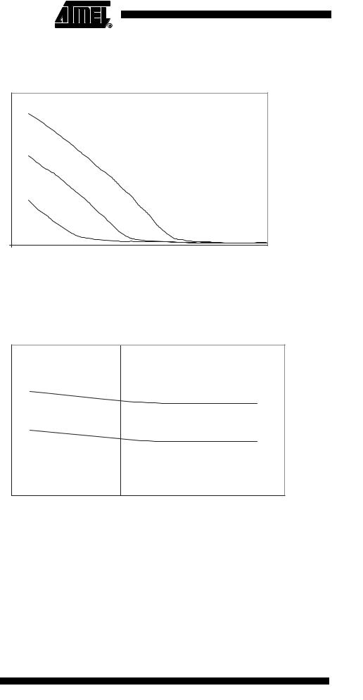
Figure 130. Reset Input Pin Hysteresis vs. VCC
RESET INPUT PIN HYSTERESIS vs. VCC
|
0.6 |
|
|
|
|
|
|
|
|
-40°C |
|
|
|
|
|
|
0.5 |
|
|
|
|
|
|
|
0.4 |
|
|
|
|
|
|
(V) |
|
25°C |
|
|
|
|
|
|
|
|
|
|
|
|
|
Threshold |
0.3 |
|
|
|
|
|
|
|
|
|
|
|
|
|
|
|
0.2 |
|
|
|
|
|
|
|
|
85°C |
|
|
|
|
|
|
0.1 |
|
|
|
|
|
|
|
0 |
|
|
|
|
|
|
|
2.5 |
3 |
3.5 |
4 |
4.5 |
5 |
5.5 |
VCC (V)
BOD Thresholds And Analog Figure 131. BOD Thresholds vs. Temperature (BOD Level is 4.0V)
Comparator Offset
BOD THRESHOLDS vs. TEMPERATURE
BODLEVEL IS 4.0V
|
4.3 |
|
|
|
|
|
|
|
|
|
|
|
|
|
|
|
|
4.2 |
|
|
|
|
|
|
|
|
|
|
|
|
|
|
|
|
|
|
|
|
|
|
|
Rising VCC |
|
|
|
|
|
|
|
|
(V) |
4.1 |
|
|
|
|
|
|
|
|
|
|
|
|
|
|
|
Threshold |
4 |
|
|
|
|
|
|
|
|
|
|
|
|
|
|
|
|
|
|
|
|
|
|
|
Falling VCC |
|
|
|
|
|
|
|
|
|
3.9 |
|
|
|
|
|
|
|
|
|
|
|
|
|
|
|
|
3.8 |
|
|
|
|
|
|
|
|
|
|
|
|
|
|
|
|
-50 |
-40 |
-30 |
-20 |
-10 |
0 |
10 |
20 |
30 |
40 |
50 |
60 |
70 |
80 |
90 |
100 |
Temperature (C)
224 ATmega8515(L)
2512G–AVR–03/05
ATmega8515(L)
Figure 132. BOD Thresholds vs. Temperature (BOD Level is 2.7V)
Threshold (V)
BOD THRESHOLDS vs. TEMPERATURE
BODLEVEL IS 2.7V
3.1
3
Rising VCC
2.9
2.8
Falling VCC
2.7
2.6
-50 -40 -30 -20 -10 |
0 |
10 20 30 40 50 60 70 80 90 100 |
Temperature (C)
Figure 133. Bandgap Voltage vs. VCC
BANDGAP VOLTAGE vs. VCC
|
1.27 |
|
|
|
|
|
|
|
1.265 |
|
|
|
|
|
-40°C |
|
|
|
|
|
|
|
|
(V) |
|
|
|
|
|
|
25°C |
Voltage |
1.26 |
|
|
|
|
|
|
|
|
|
|
|
|
||
|
|
|
|
|
|
85°C |
|
|
|
|
|
|
|
|
|
Bandgap |
1.255 |
|
|
|
|
|
|
|
|
|
|
|
|
|
|
|
1.25 |
|
|
|
|
|
|
|
1.245 |
|
|
|
|
|
|
|
2.5 |
3 |
3.5 |
4 |
4.5 |
5 |
5.5 |
Vcc (V)
225
2512G–AVR–03/05
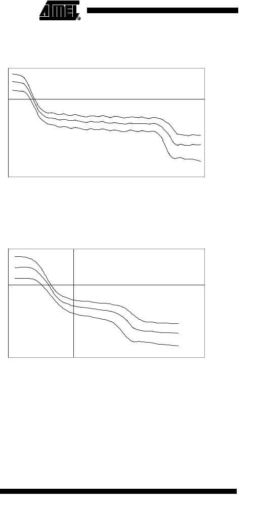
Figure 134. Analog Comparator Offset Voltage vs. Common Mode Voltage (VCC = 5V)
ANALOG COMPARATOR OFFSET VOLTAGE vs. COMMON MODE VOLTAGE
|
|
|
|
|
|
Vcc = 5V |
|
|
|
|
|
|
0.002 |
|
|
|
|
|
|
|
|
|
|
|
0.001 |
|
|
|
|
|
|
|
|
|
|
(V) |
0 |
|
|
|
|
|
|
|
|
|
|
Voltage |
|
|
|
|
|
|
|
|
|
|
|
-0.001 |
|
|
|
|
|
|
|
|
|
|
|
Offset |
|
|
|
|
|
|
|
|
|
|
|
-0.002 |
|
|
|
|
|
|
|
|
|
|
|
Comparator |
|
|
|
|
|
|
|
|
|
|
|
|
|
|
|
|
|
|
|
|
|
85°C |
|
-0.003 |
|
|
|
|
|
|
|
|
|
25°C |
|
|
|
|
|
|
|
|
|
|
|
|
|
|
-0.004 |
|
|
|
|
|
|
|
|
|
-40°C |
|
-0.005 |
|
|
|
|
|
|
|
|
|
|
|
0 |
0.5 |
1 |
1.5 |
2 |
2.5 |
3 |
3.5 |
4 |
4.5 |
5 |
Common Mode Voltage (V)
Figure 135. Analog Comparator Offset Voltage vs. Common Mode Voltage(VCC = 2.7V)
ANALOG COMPARATOR OFFSET VOLTAGE vs. COMMON MODE VOLTAGE
|
0.002 |
|
|
Vcc = 2.7V |
|
|
|
|
|
|
|
|
|
|
|
|
0.001 |
|
|
|
|
|
|
(V) |
|
|
|
|
|
|
|
Voltage |
0 |
|
|
|
|
|
|
|
|
|
|
|
|
|
|
Offset |
-0.001 |
|
|
|
|
|
|
|
|
|
|
|
|
|
|
Comparator |
-0.002 |
|
|
|
|
|
85°C |
|
|
|
|
|
|
||
|
|
|
|
|
|
25°C |
|
|
-0.003 |
|
|
|
|
|
|
|
|
|
|
|
|
|
|
|
|
|
|
|
|
|
-40°C |
|
-0.004 |
|
|
|
|
|
|
|
0 |
0.5 |
1 |
1.5 |
2 |
2.5 |
3 |
Common Mode Voltage (V)
226 ATmega8515(L)
2512G–AVR–03/05